Versatile Voltage-Mode Biquadratic Filter and Quadrature Oscillator Using Four OTAs and Two Grounded Capacitors


Abstract
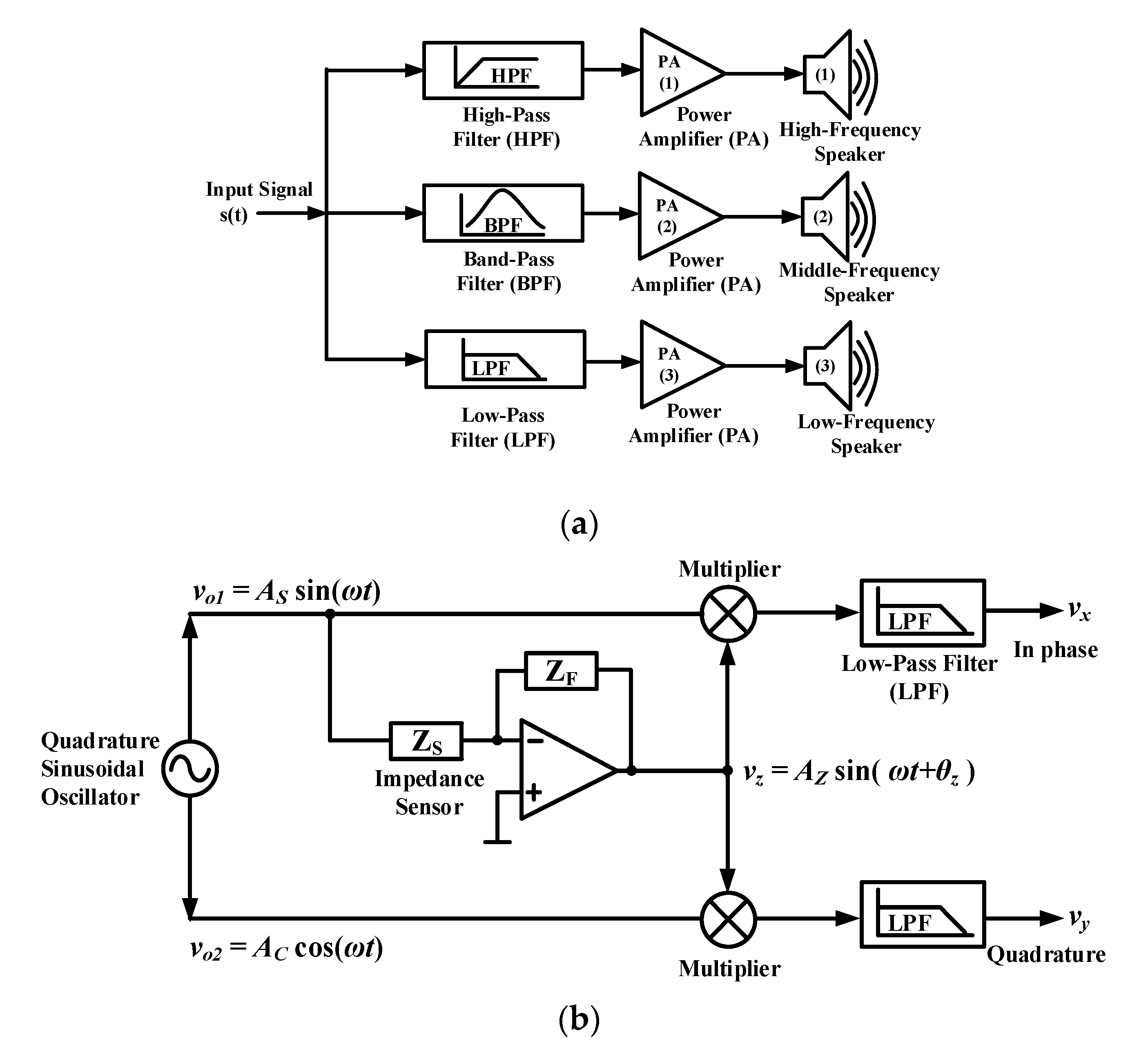
:1. Introduction
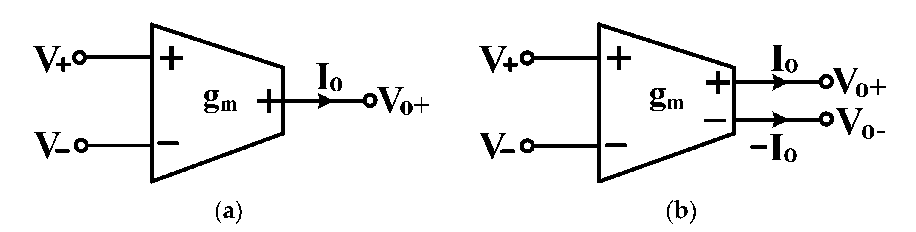
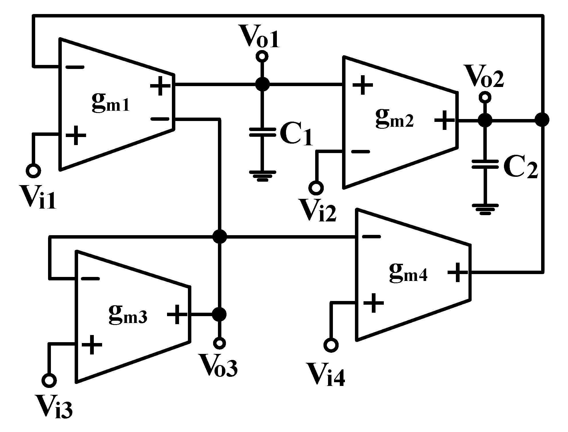
2. Circuit Descriptions
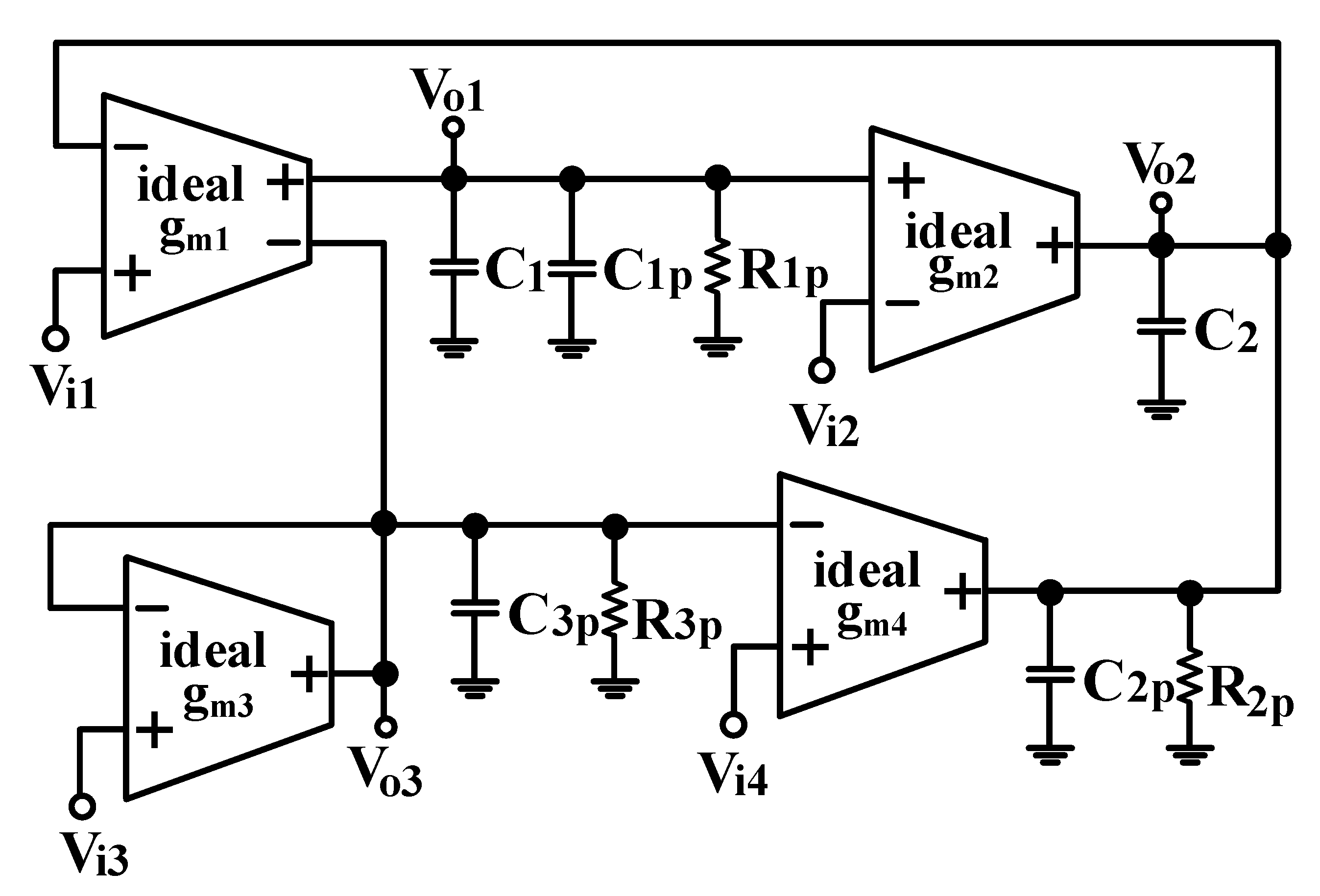
2.1. Proposed Versatile VM Biquad Filter
- (1)
- LP filter: Vi1 = Vi3 = Vin, and Vi2 = Vi4 = 0.
- (2)
- IBP filter: Vi2 = Vin, and Vi1 = Vi3 = Vi4 = 0.
- (3)
- BP filter: Vi4 = Vin, and Vi1 = Vi2 = Vi3 = 0.
- (4)
- IHP filter: Vi1 = Vin, and Vi2 = Vi3 = Vi4 = 0.
- (5)
- BR filter: Vi3 = Vin, and Vi1 = Vi2 = Vi4 = 0.
- (6)
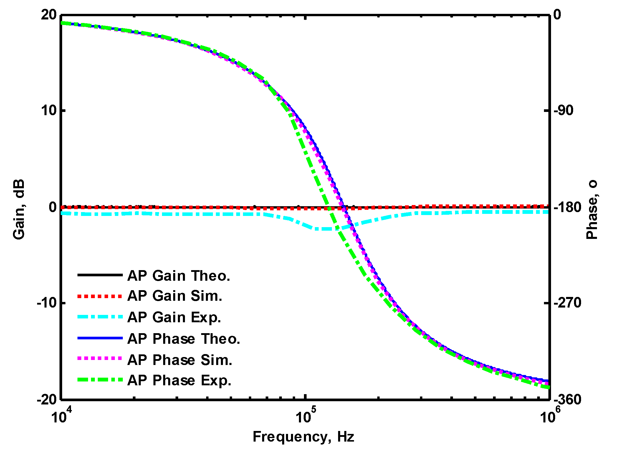
- AP filter: Vi2 = Vi3 = Vin, and Vi1 = Vi4 = 0.
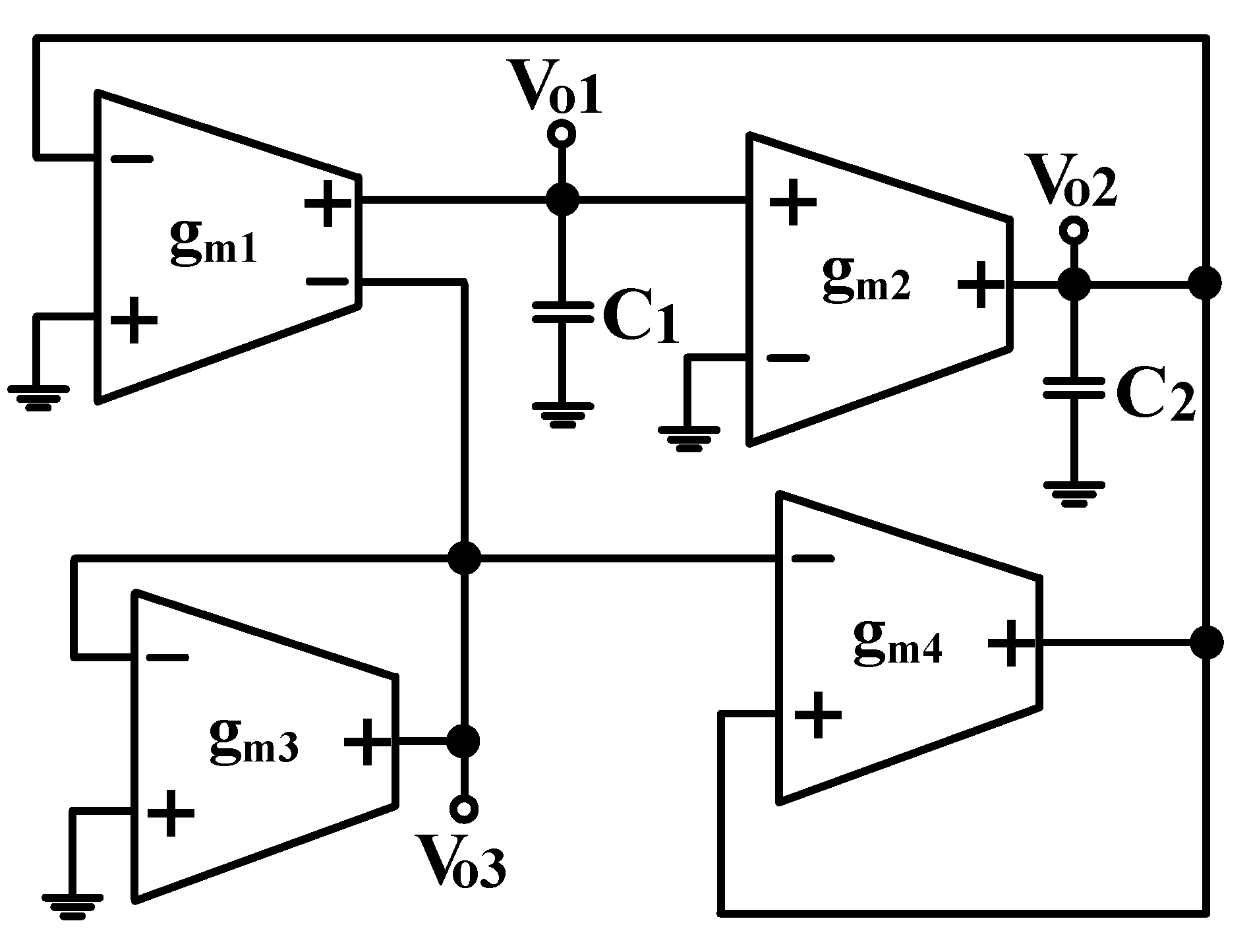
2.2. Modification of Proposed Filter as VM Quadrature Oscillator
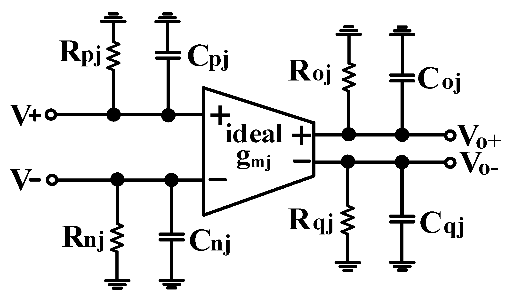
3. Effect of the Parasitic Impedances in OTA
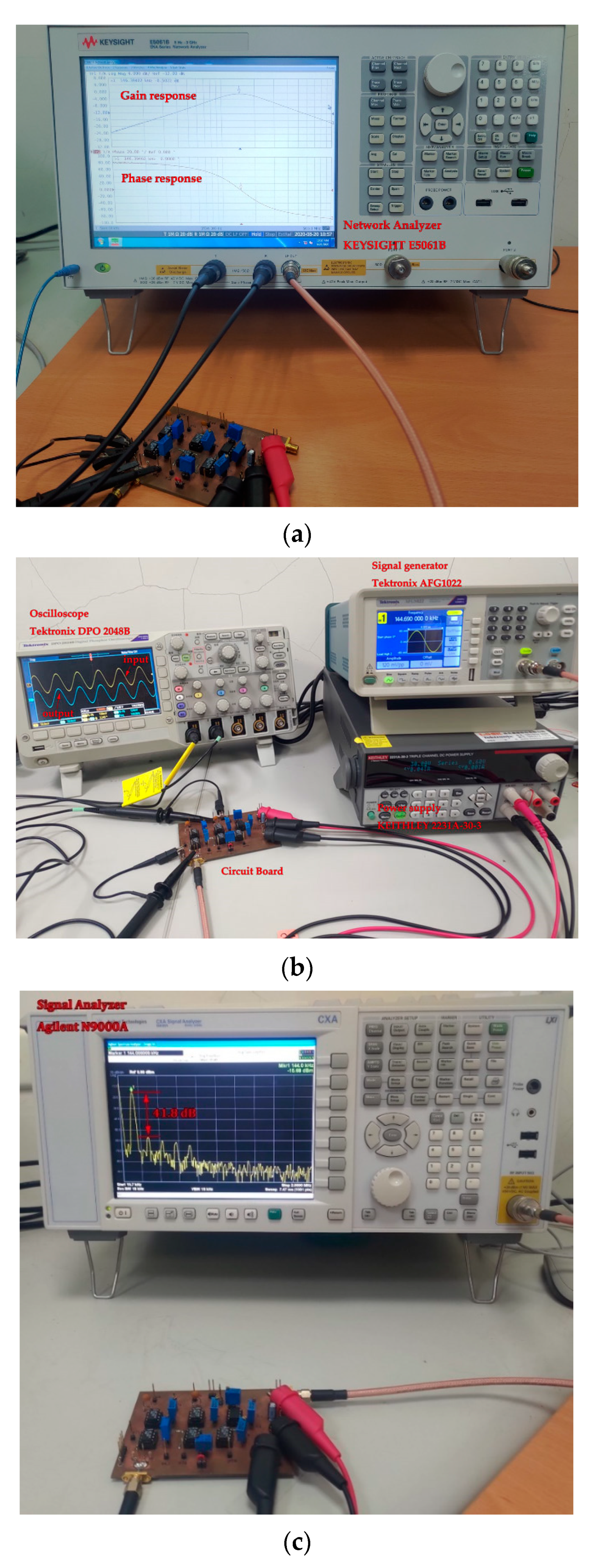
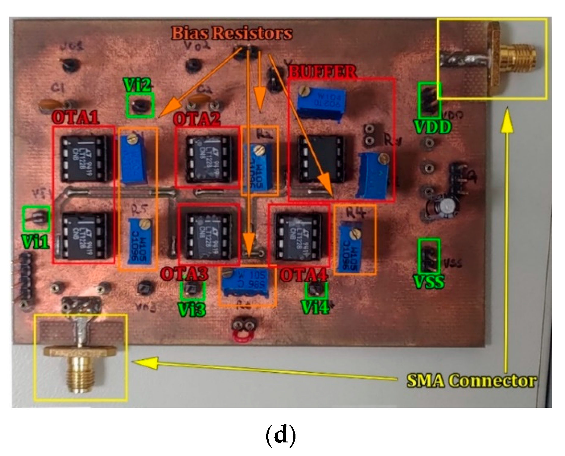
4. Simulation and Experimental Results
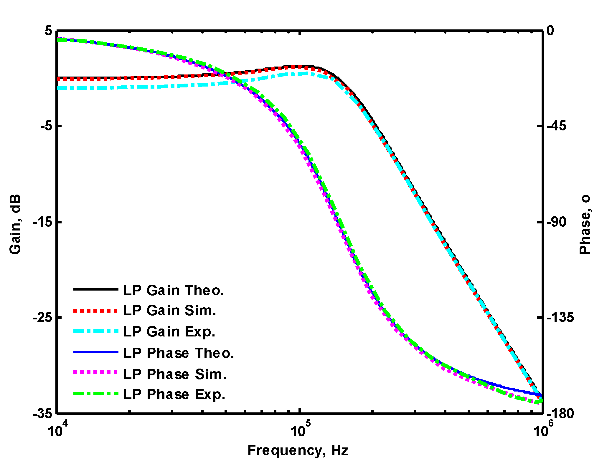
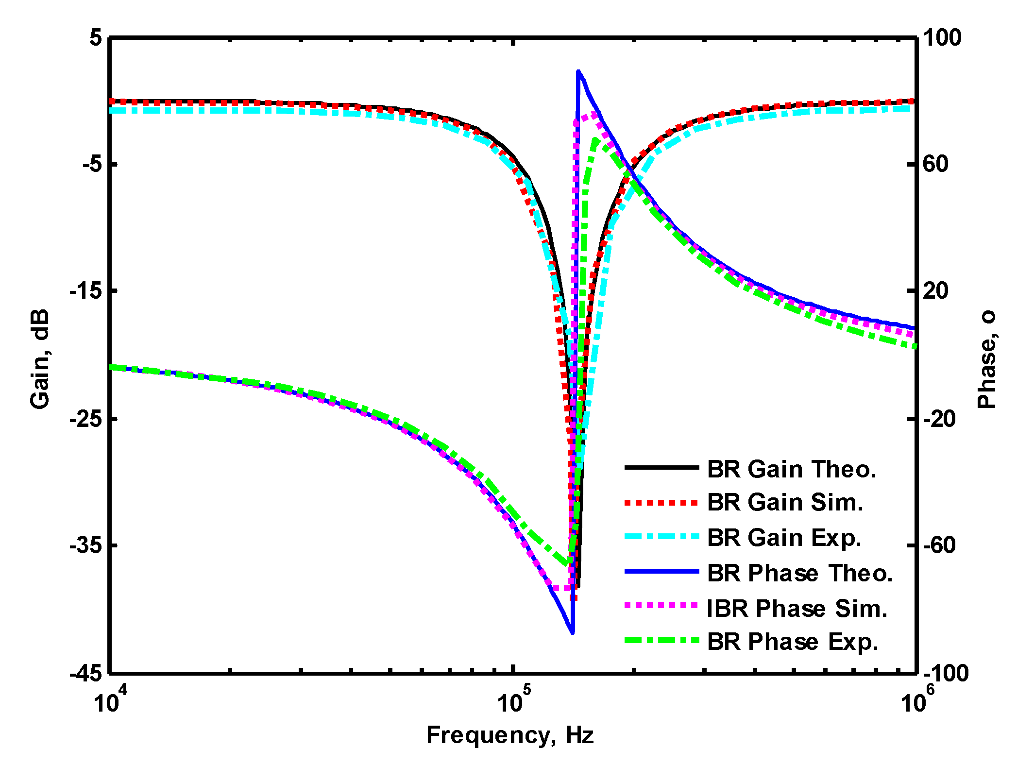
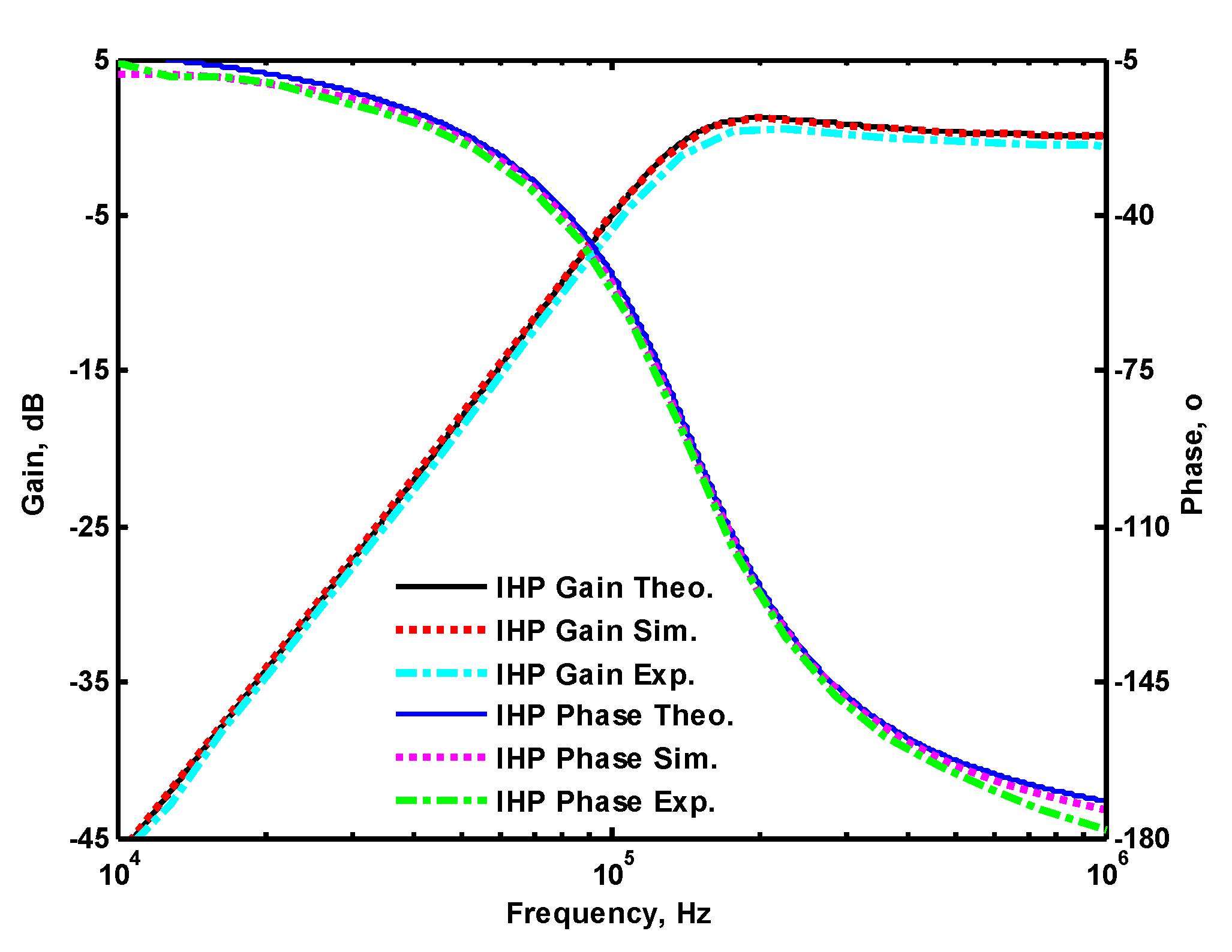
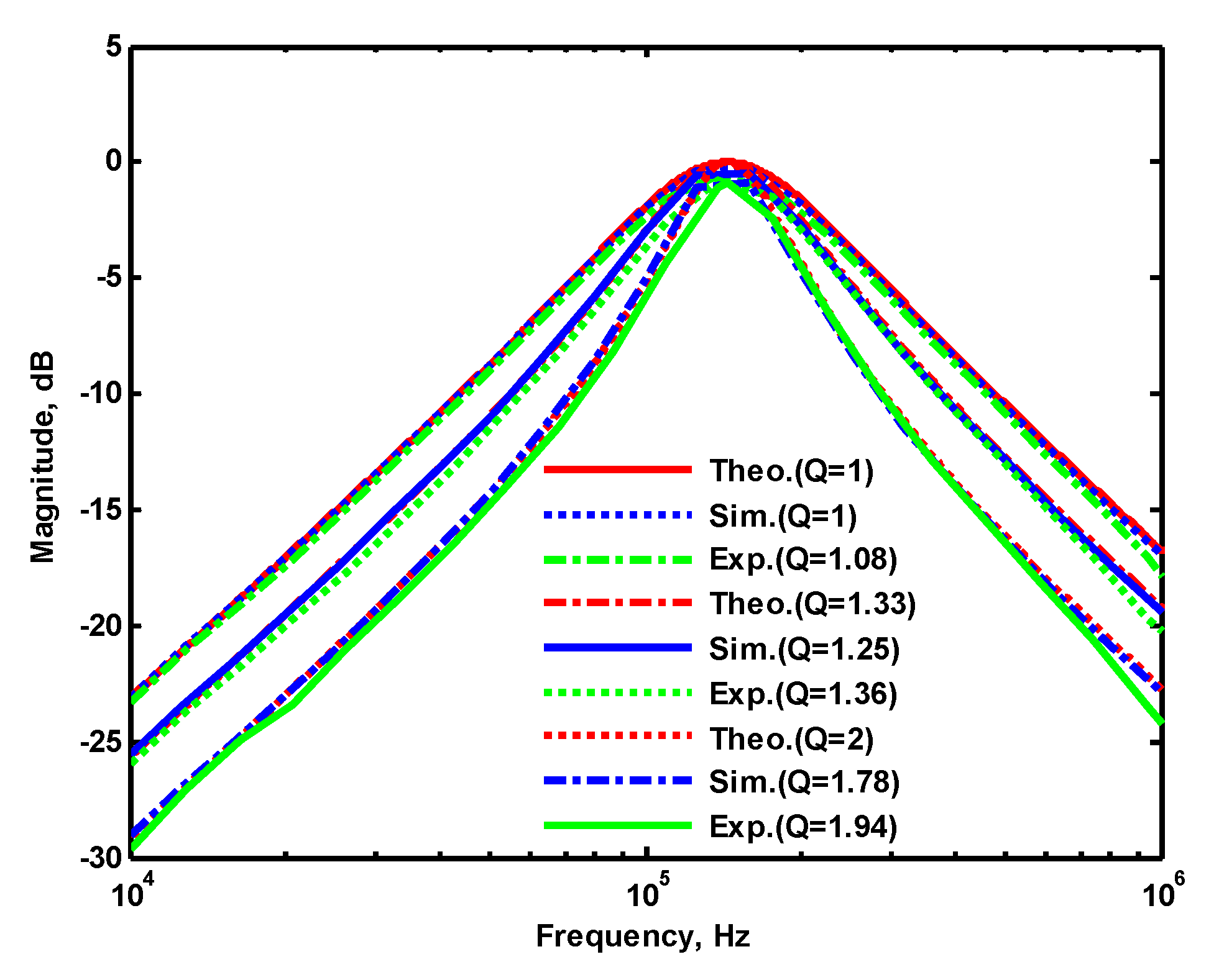
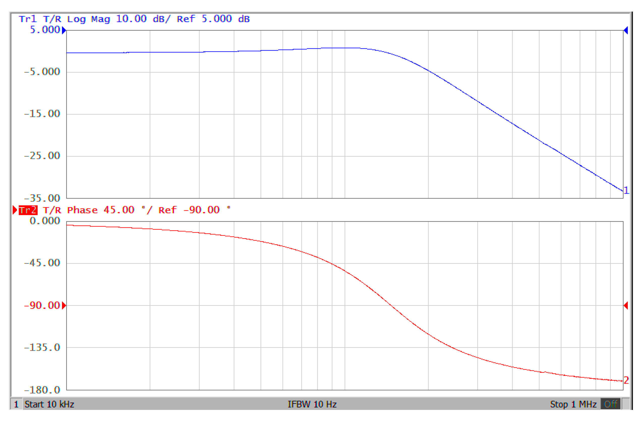
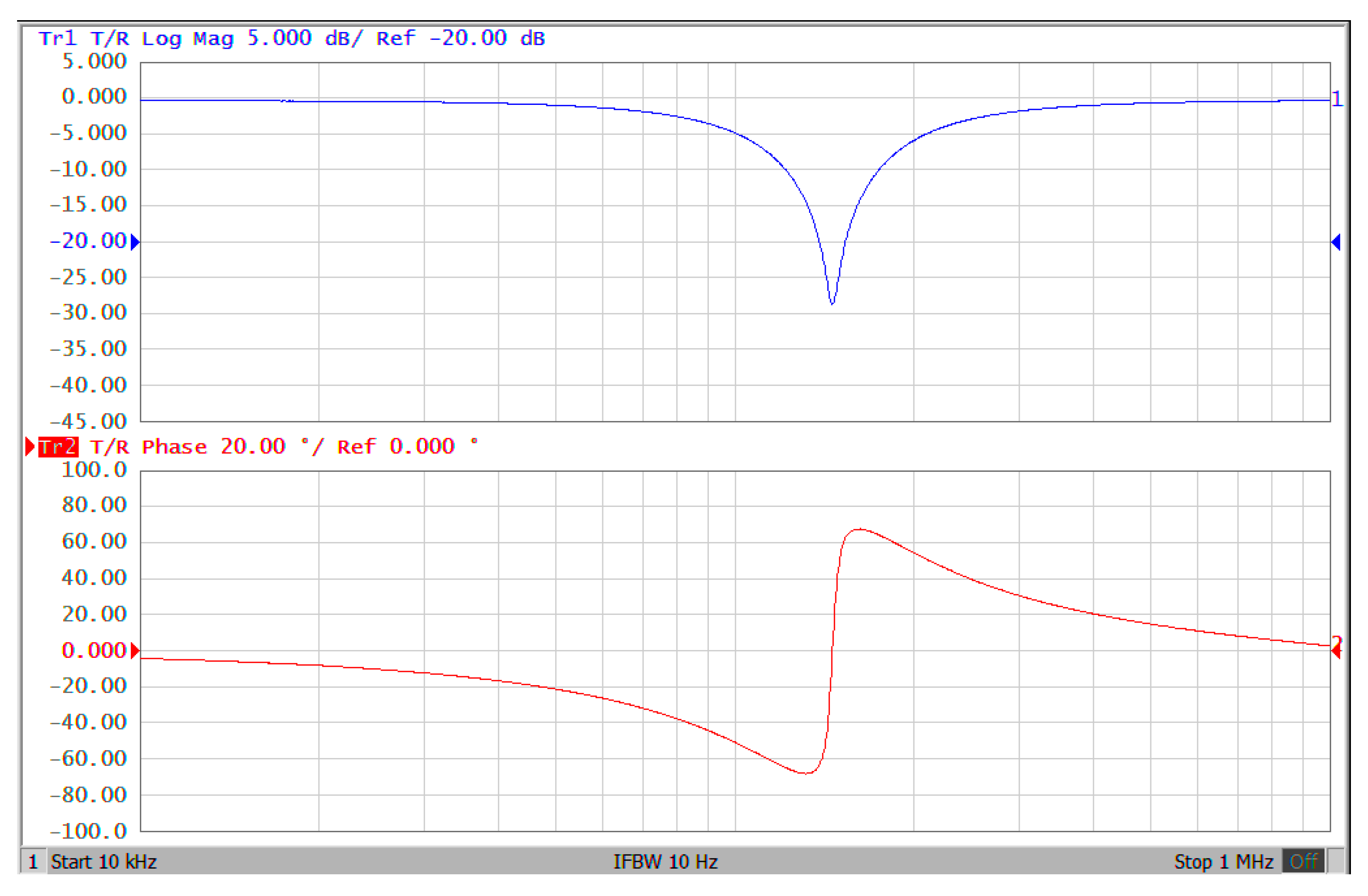
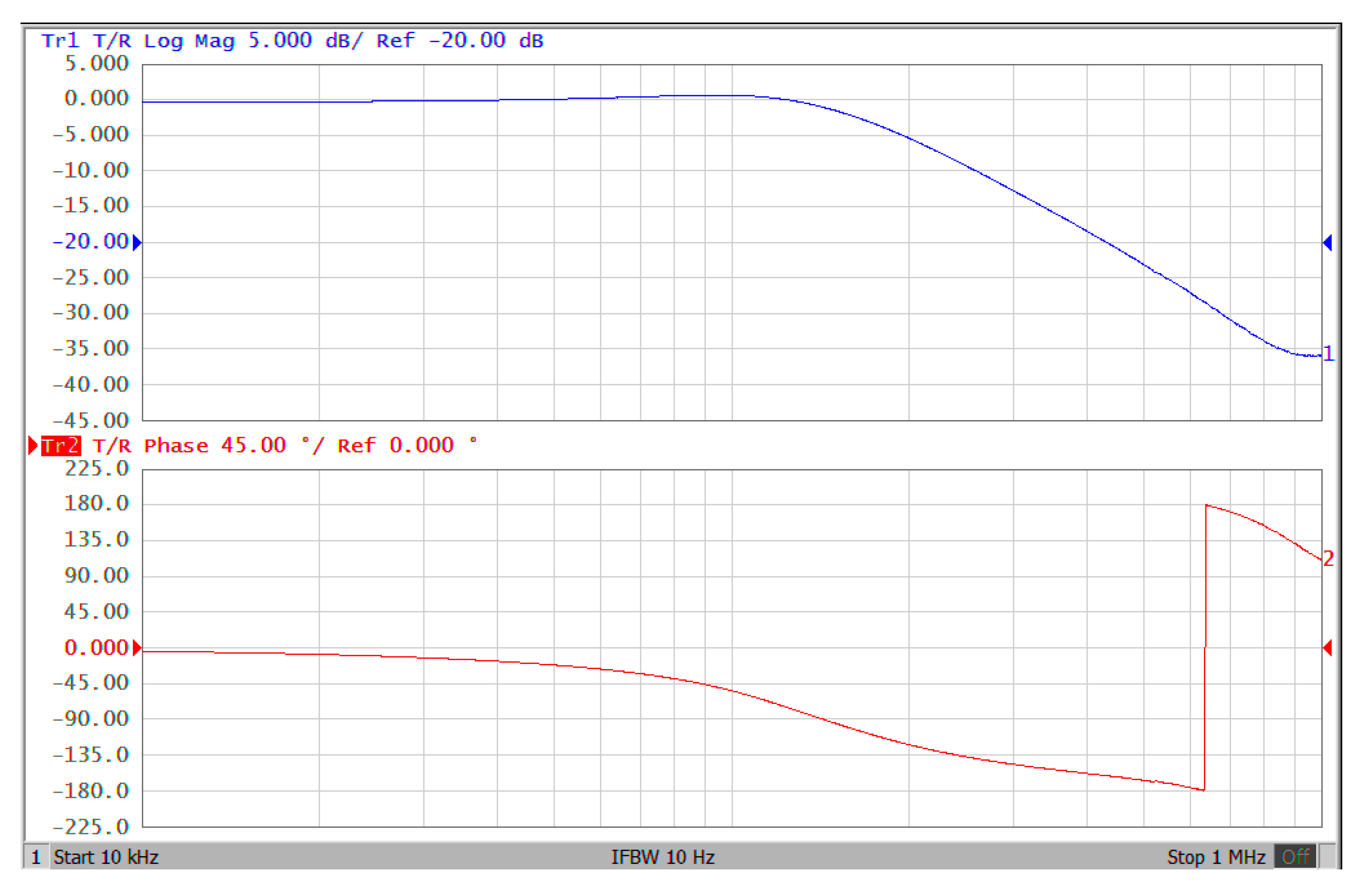
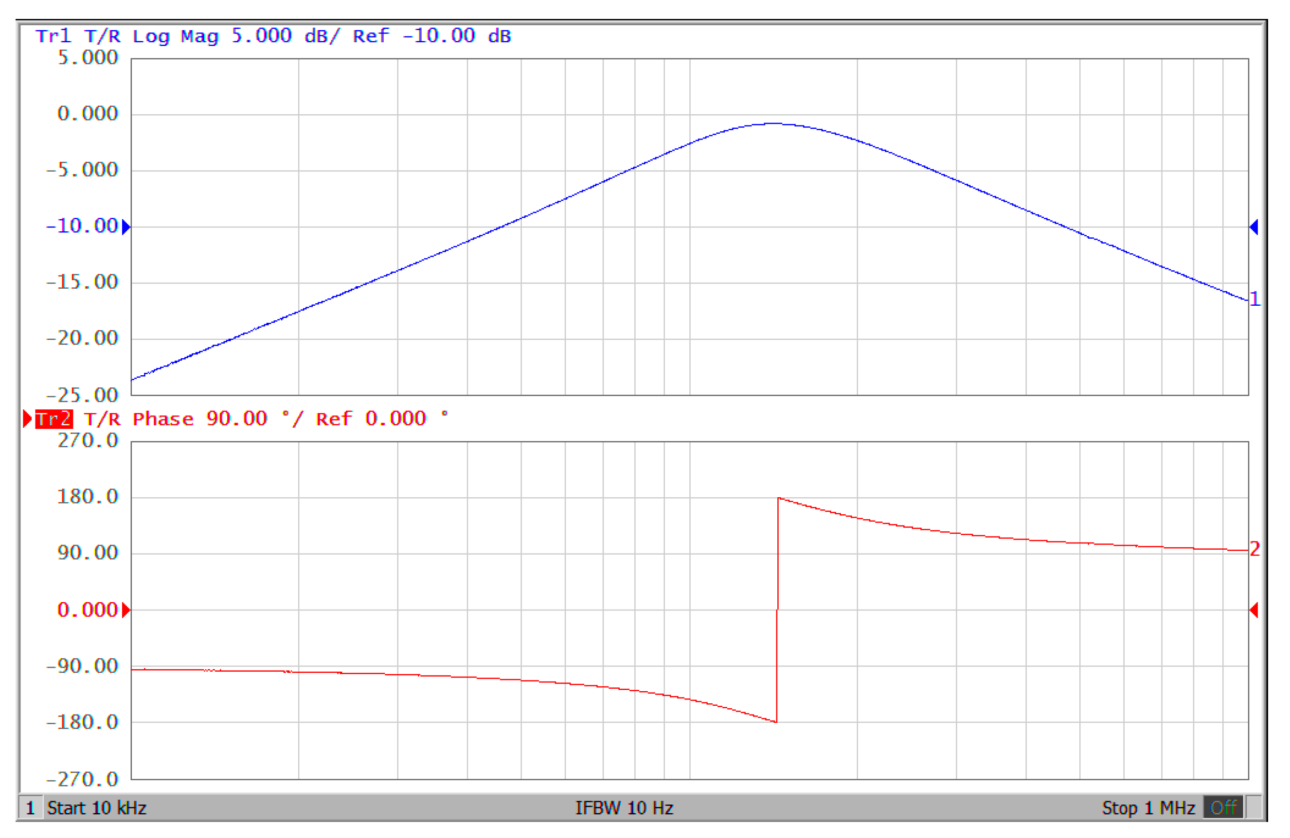
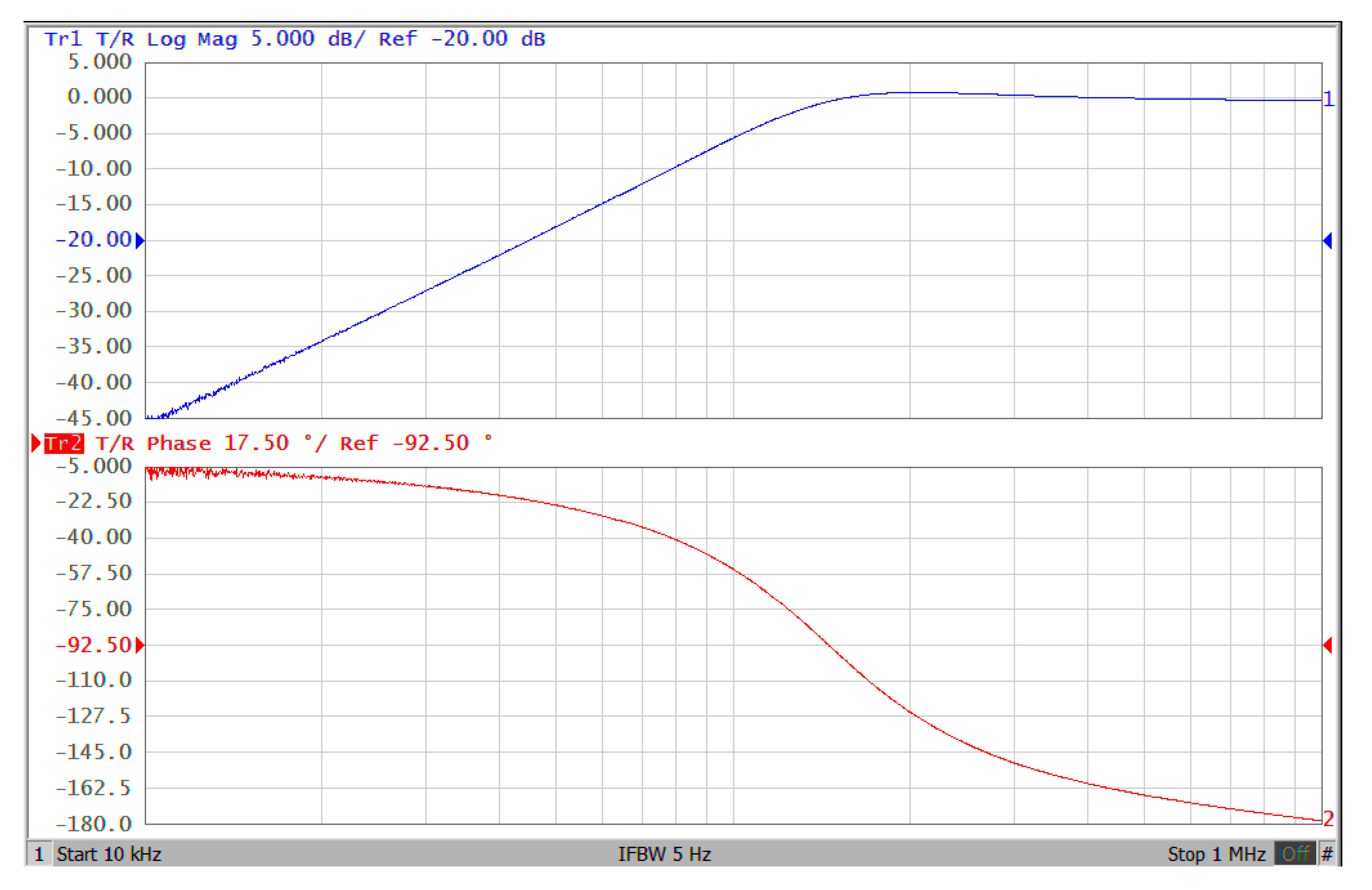
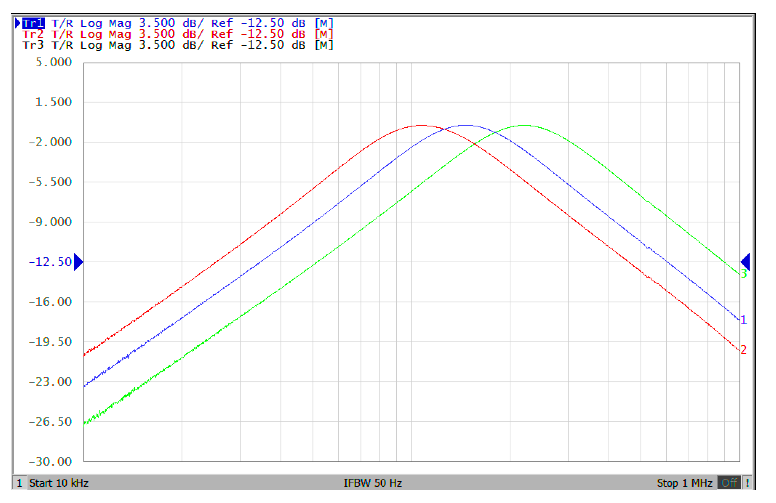
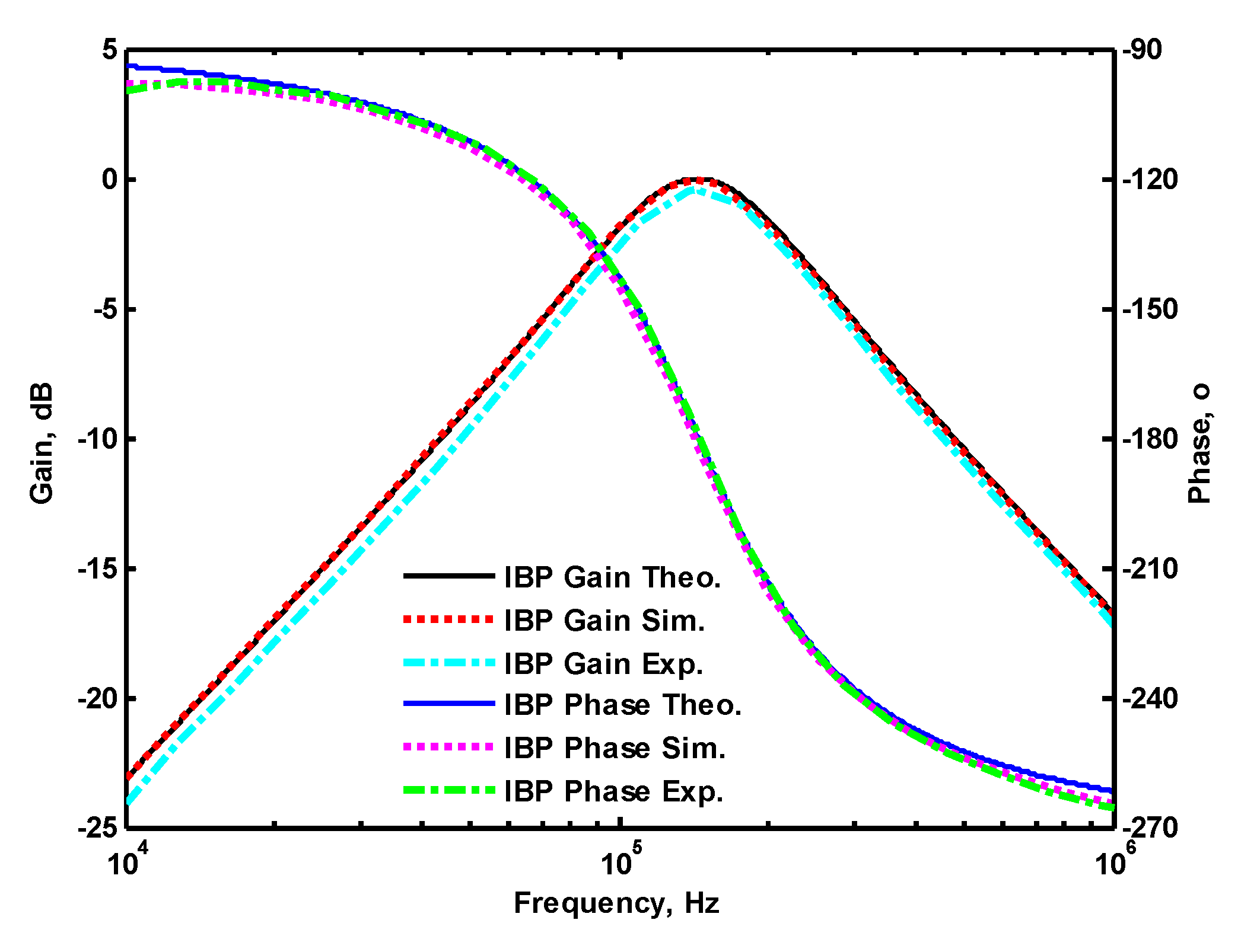
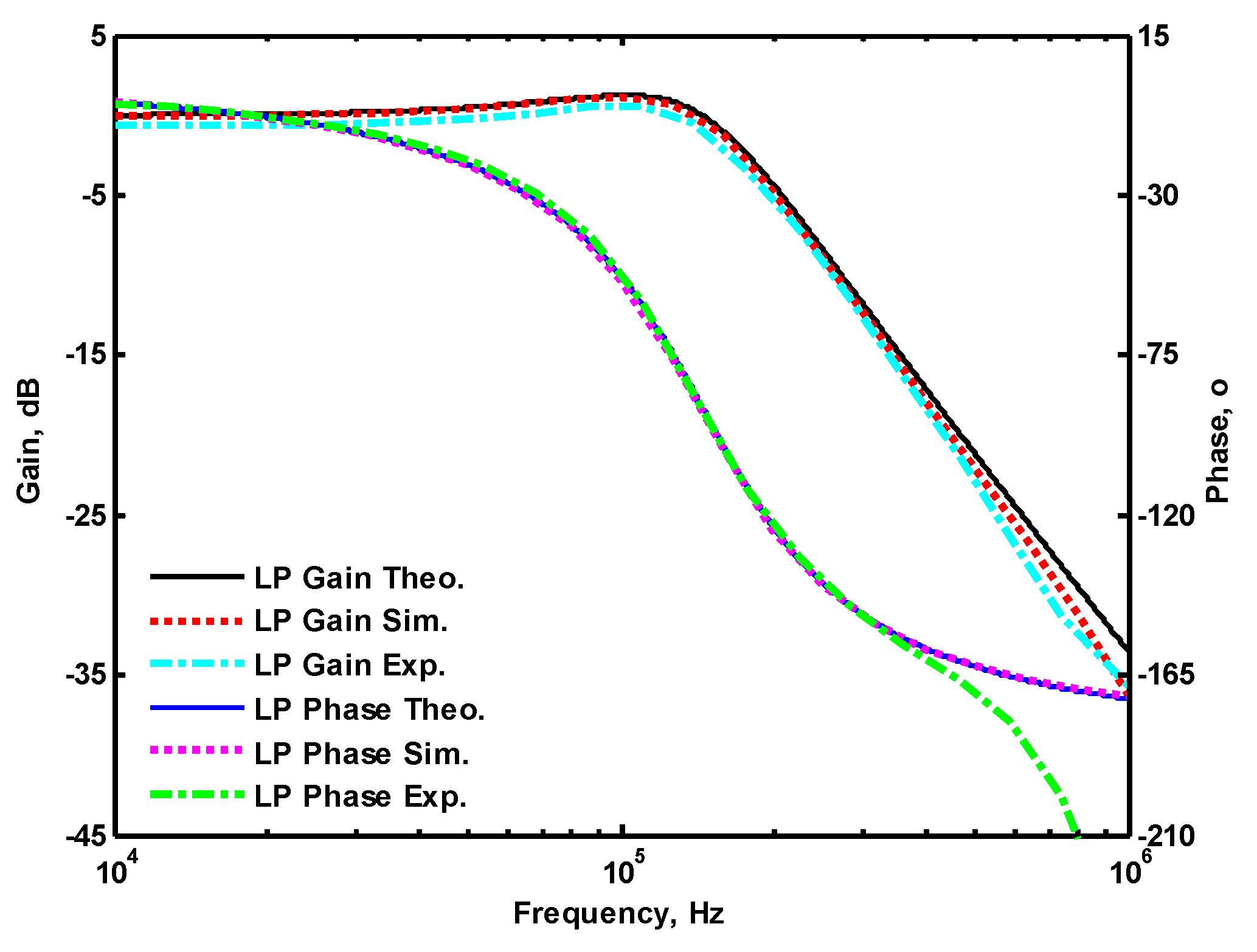
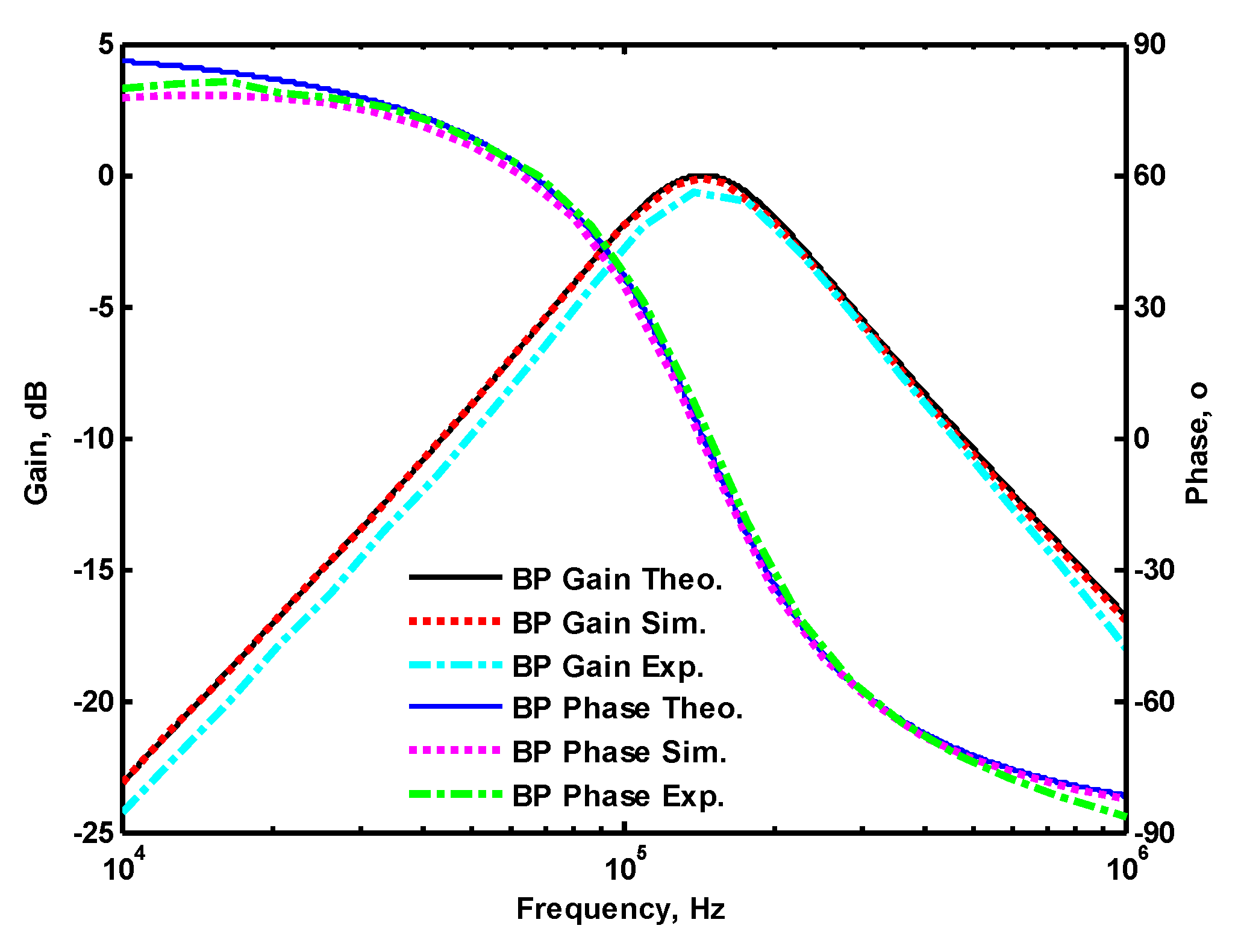
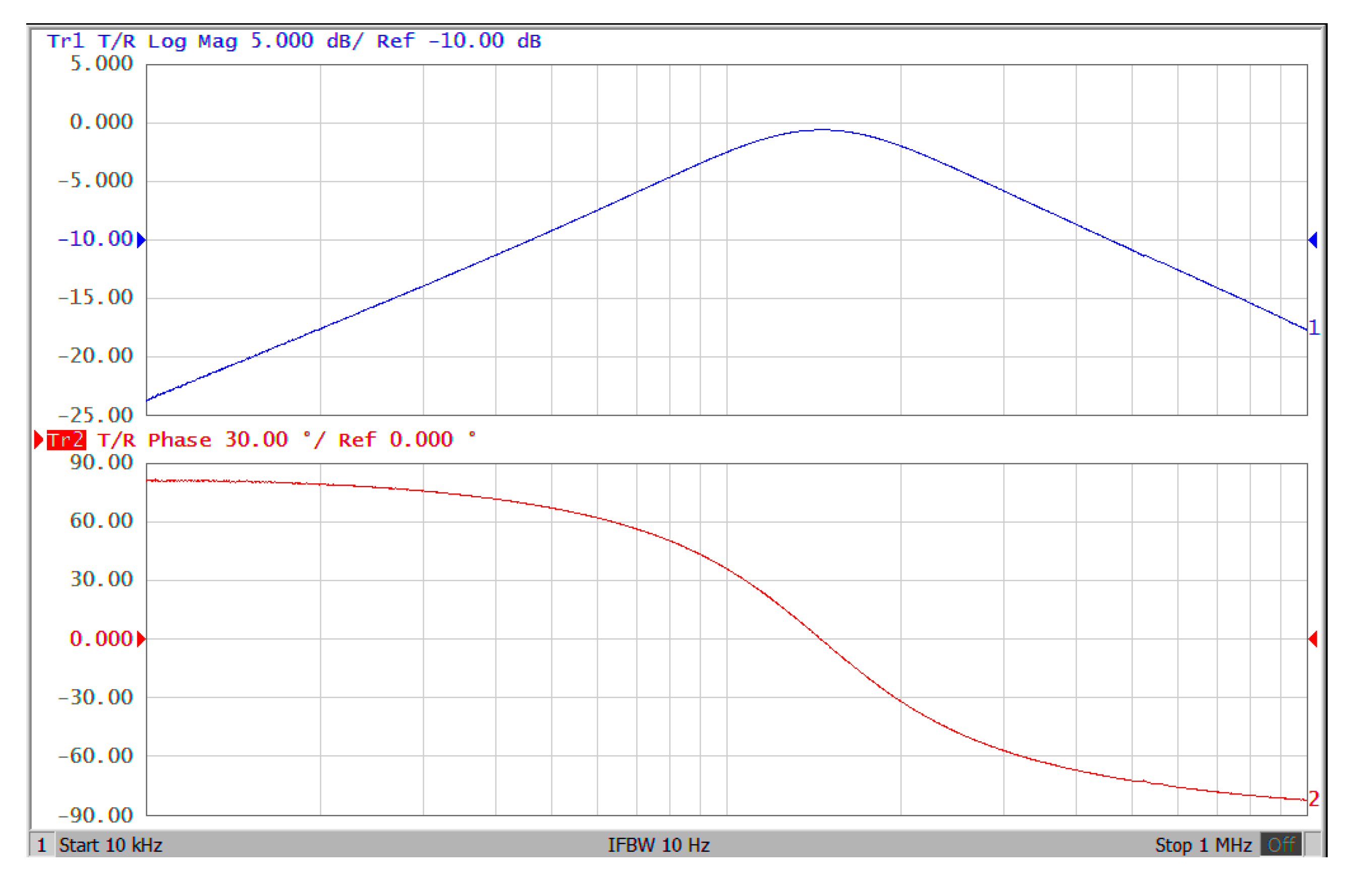
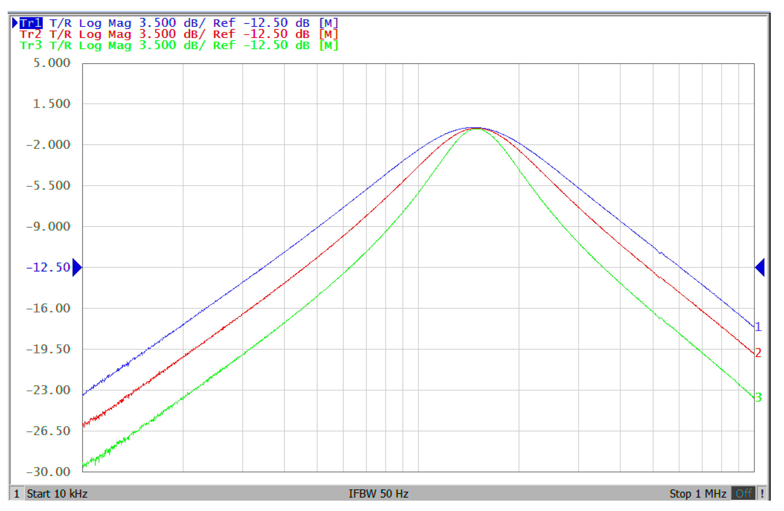
4.1. Versatile VM Biquad Filter Simulation and Experimental Results
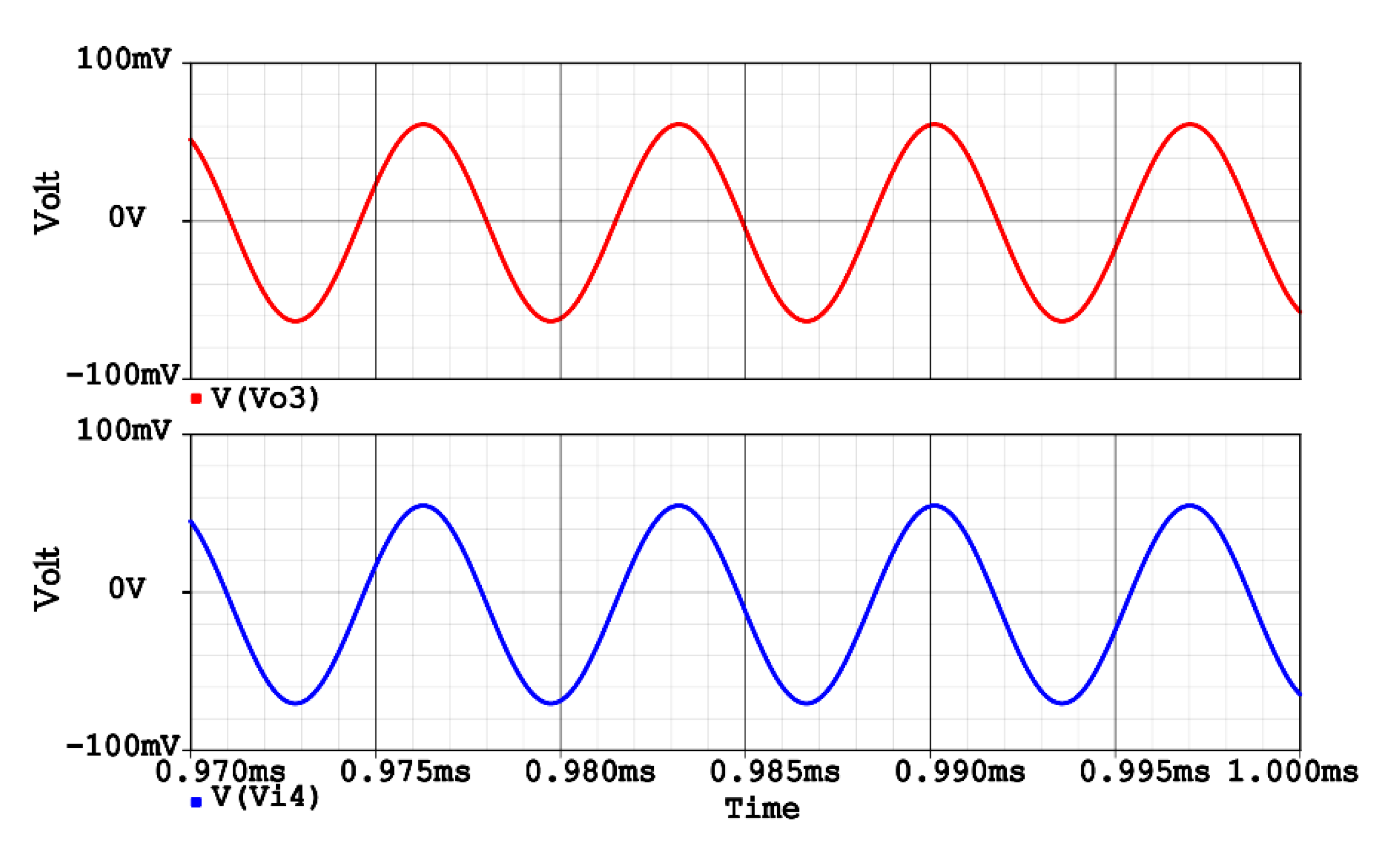
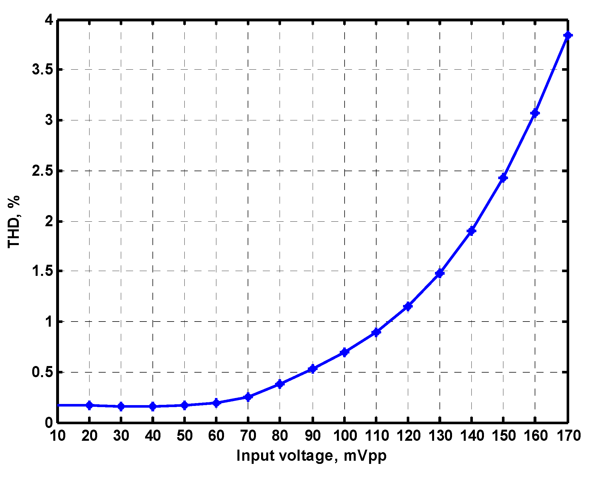
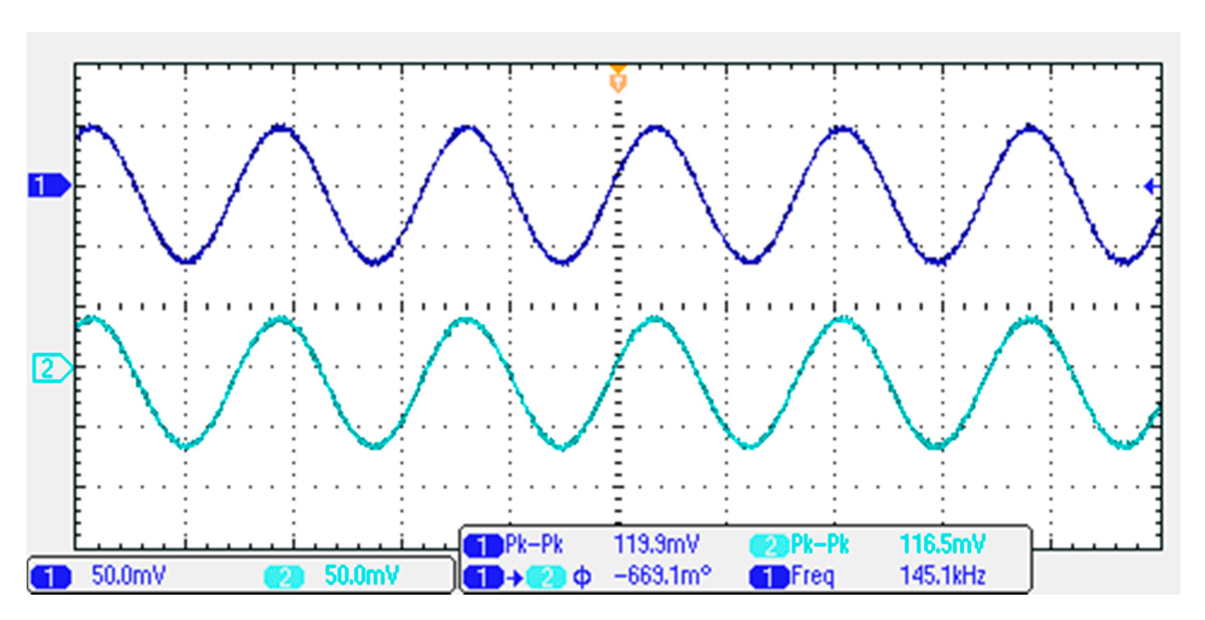
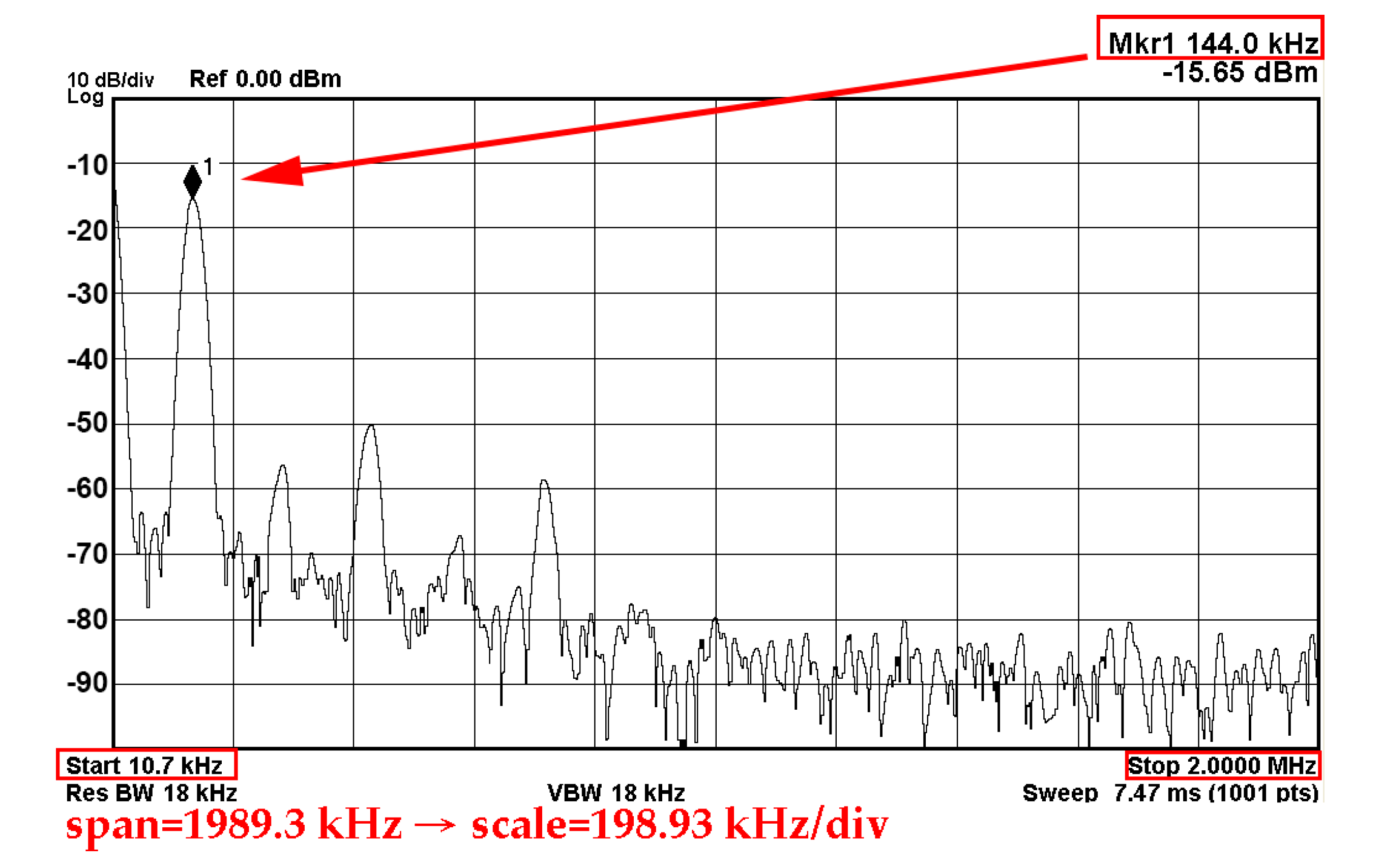
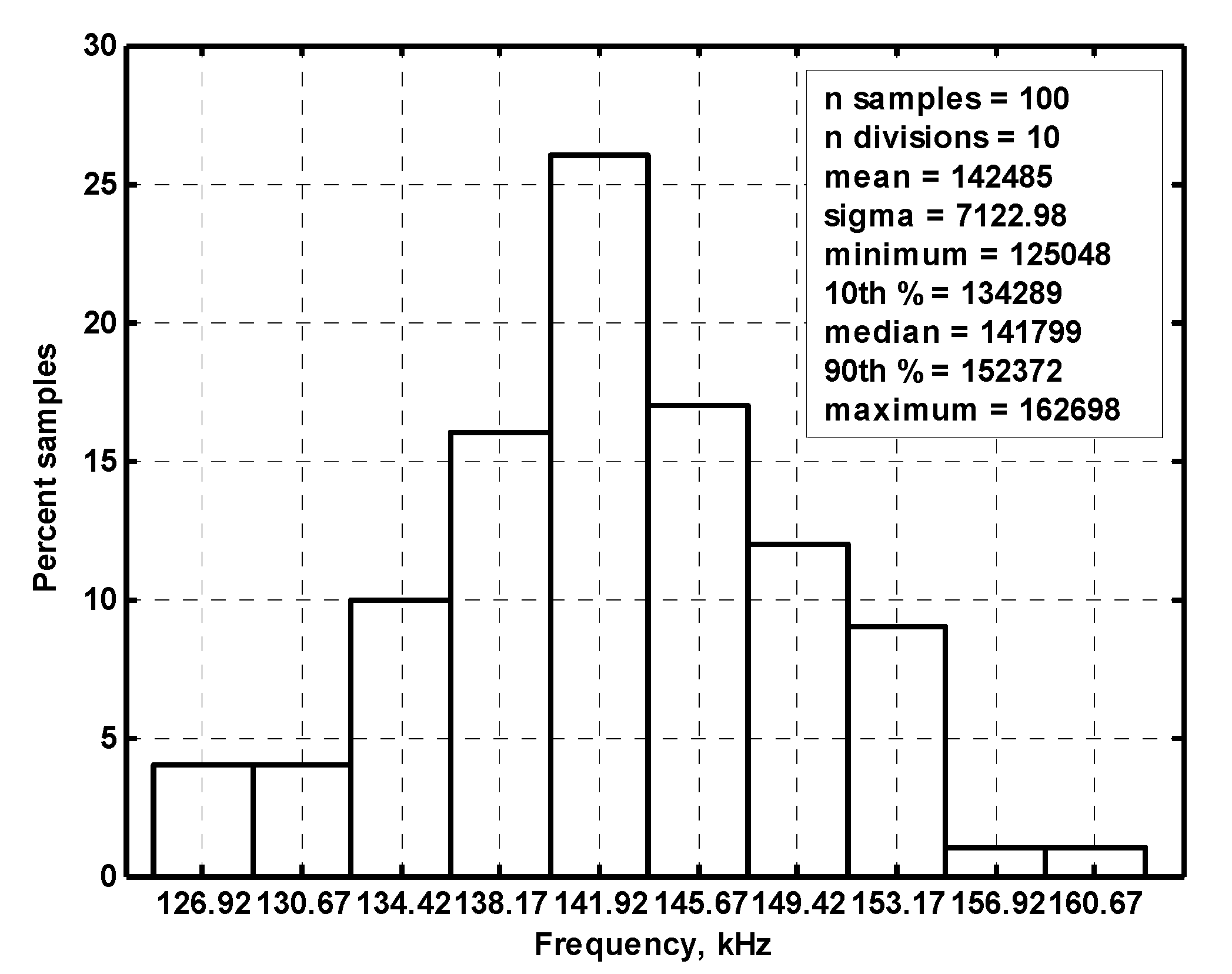
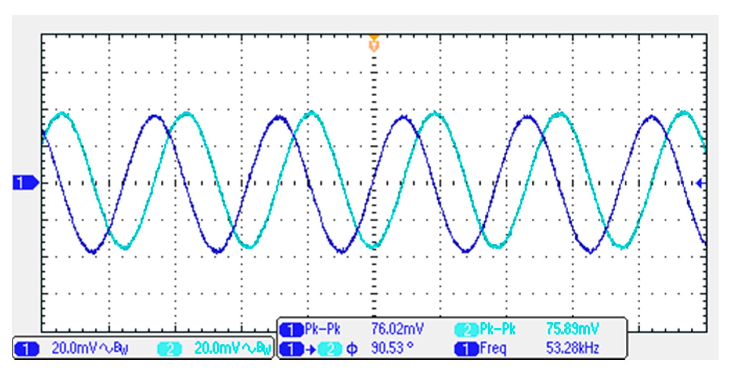
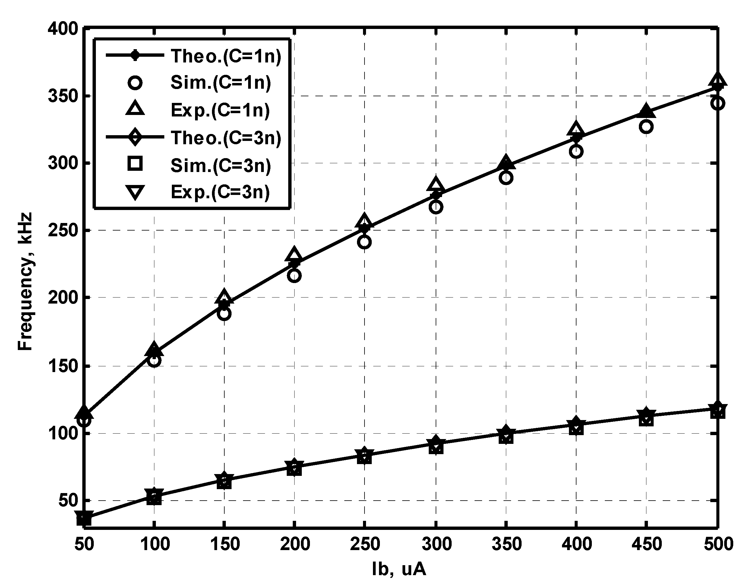
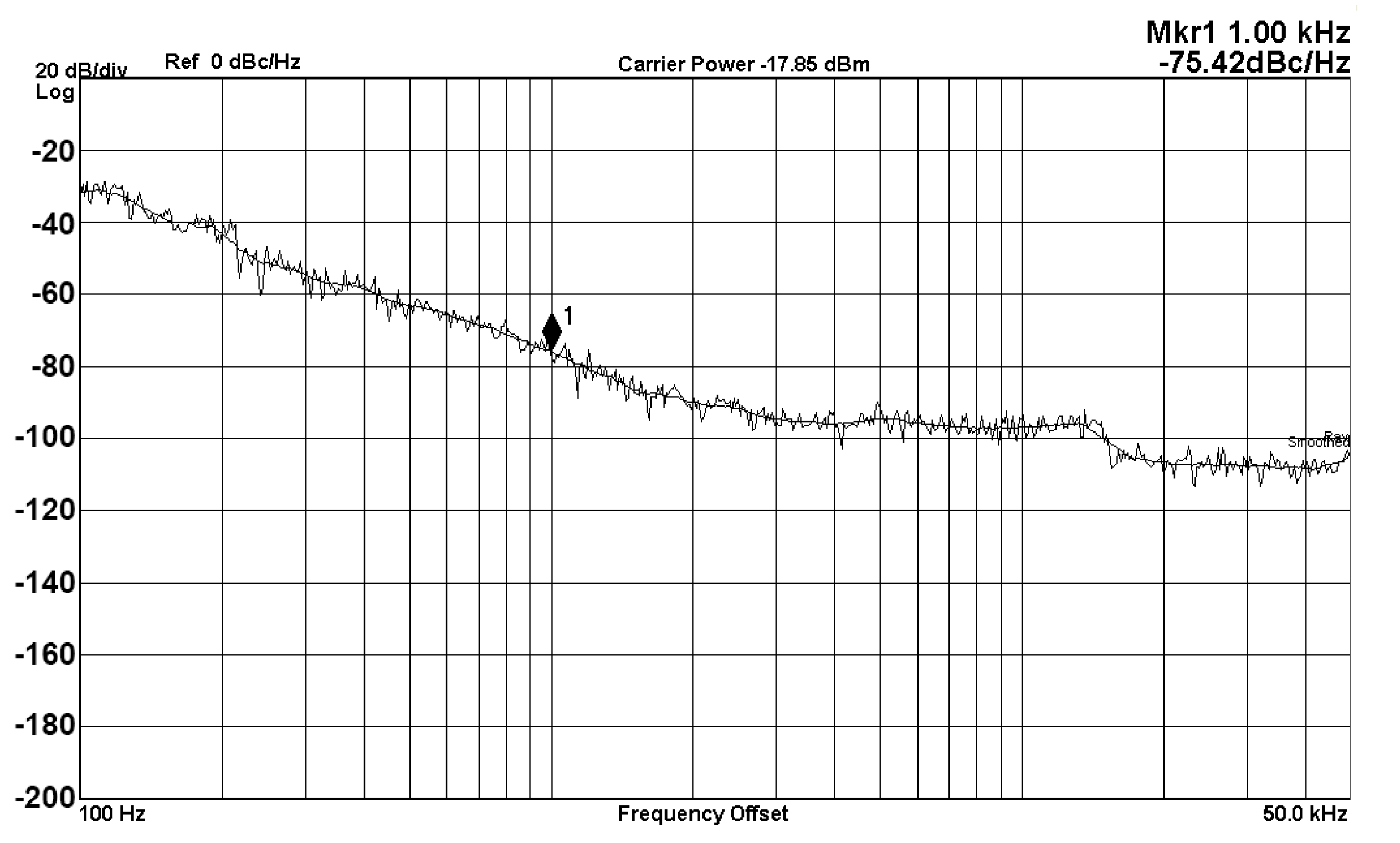
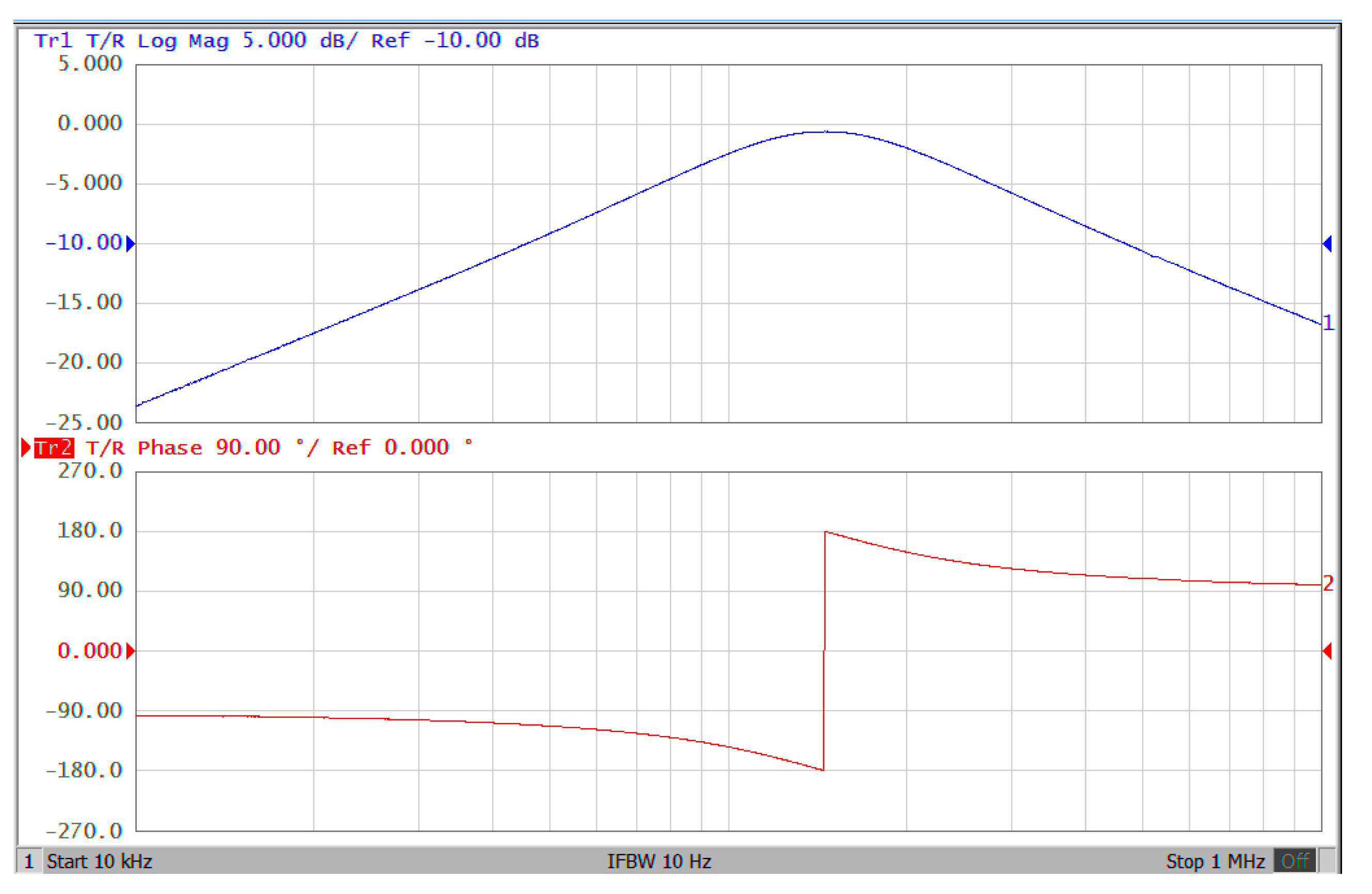
4.2. VM Quadrature Oscillator Simulation and Experimental Results
5. Conclusions
Author Contributions
Funding
Conflicts of Interest
References
- Wang, H.Y.; Tran, H.D.; Nguyen, Q.M.; Yin, L.-T.; Liu, C.Y. Derivation of oscillators from biquadratic band pass filters using circuit transformations. Appl. Sci. 2014, 4, 482–492. [Google Scholar] [CrossRef]
- Singh, V.K.; Singh, A.K.; Bhaskar, D.R.; Senani, R. New universal biquads employing CFOAs. IEEE Trans. Circuits Syst. II Express Briefs 2006, 53, 1299–1303. [Google Scholar] [CrossRef]
- Márquez, A.; Pérez-Bailón, J.; Calvo, B.; Medrano, N.; Martínez, P.A. A CMOS self-contained quadrature signal generator for SoC impedance spectroscopy. Sensors 2018, 18, 1382. [Google Scholar] [CrossRef] [PubMed] [Green Version]
- Ibrahim, M.A.; Minaei, S.; Kuntman, H.A. A 22.5 MHz current-mode KHN-biquad using differential voltage current conveyor and grounded passive elements. AEU Int. J. Electron. Commun. 2005, 59, 311–318. [Google Scholar] [CrossRef]
- Jaikla, W.; Adhan, S.; Suwanjan, P.; Kumngern, M. Current/voltage controlled quadrature sinusoidal oscillators for phase sensitive detection using commercially available IC. Sensors 2020, 20, 1319. [Google Scholar] [CrossRef] [Green Version]
- Horng, J.W. High input impedance voltage-mode universal biquadratic filter using two OTAs and one CCII. Int. J. Electron. 2003, 90, 185–191. [Google Scholar] [CrossRef]
- Horng, J.W.; Hsu, C.H.; Tseng, C.Y. High input impedance voltage-mode universal biquadratic filters with three inputs using three CCs and grounding capacitors. Radioengineering 2012, 21, 290–296. [Google Scholar]
- Horng, J.W. Voltage-mode multifunction biquadratic filter employing single DVCC. Int. J. Electron. 2012, 99, 153–162. [Google Scholar] [CrossRef]
- Chen, H.P.; Shen, S.S.; Wang, J.P. Electronically tunable versatile voltage-mode universal filter. AEU Int. J. Electron. Commun. 2008, 62, 316–319. [Google Scholar] [CrossRef]
- Chen, H.P. Versatile multifunction universal voltage-mode biquadratic filter. AEU Int. J. Electron. Commun. 2010, 64, 983–987. [Google Scholar] [CrossRef]
- Lee, C.N. Independently tunable plus-type DDCC-based voltage-mode universal biquad filter with MISO and SIMO types. Microelectron. J. 2017, 67, 71–81. [Google Scholar] [CrossRef]
- Minaei, S.; Sayin, O.K.; Kuntman, H. A new CMOS electronically tunable current conveyor and its application to current-mode filters. IEEE Trans. Circuits Syst. I 2006, 53, 1448–1457. [Google Scholar] [CrossRef]
- Masud, M.; A’ain, A.; Khan, I.; Husin, N. Design of voltage mode electronically tunable first order all pass filter in ±0.7 V 16 nm CNFET Technology. Electronics 2019, 8, 95. [Google Scholar] [CrossRef] [Green Version]
- Zhang, C.; Shang, L.; Wang, Y.; Tang, L. A CMOS programmable fourth-order butterworth active-RC low-pass filter. Electronics 2020, 9, 204. [Google Scholar] [CrossRef] [Green Version]
- Acosta, L.; Jimenez, M.; Carvajal, R.G.; Lopez-Martin, A.J.; Ramirez-Angulo, J. Highly linear tunable CMOS gm-C low-pass filter. IEEE Trans. Circuits Syst. I Regul. Pap. 2009, 56, 2145–2158. [Google Scholar] [CrossRef]
- Acar, C.; Naday, F.; Kuntman, H. On the realization of OTA-C filter. Int. J. Circuit Appl. 1993, 21, 331–341. [Google Scholar] [CrossRef]
- Chang, C.M.; Soliman, A.M.; Swamy, M.N.S. Analytical synthesis of low-sensitivity high-order voltage-mode DDCC and FDCCII-grounded R and C all-pass filter structures. IEEE Trans. Circuits Syst. I Regul. Pap. 2007, 54, 1430–1443. [Google Scholar] [CrossRef]
- Hwang, Y.S.; Kung, C.M.; Lin, H.C.; Chen, J.J. Low-sensitivity, low-bounce, high-linearity current-controlled oscillator suitable for single-supply mixed-mode instrumentation system. IEEE Trans. Ultrason. Ferroelectr. Freq. Control 2009, 56, 254–262. [Google Scholar] [CrossRef]
- Hwang, Y.S.; Liu, W.H.; Tu, S.H.; Chen, J.J. New building block: Multiplication-mode current conveyor. IET Circuits Devices Syst. 2009, 3, 41–48. [Google Scholar] [CrossRef]
- Tu, S.H.; Hwang, Y.S.; Chen, J.J.; Soliman, A.M.; Chang, C.M. OTA-C arbitrary-phase-shift oscillators. IEEE Trans. Instrum. Meas. 2012, 61, 2305–2319. [Google Scholar] [CrossRef]
- Nikoofard, A.; Kananian, S.; Fotowat-Ahmady, A. Off-resonance oscillation, phase retention, and orthogonality modeling in quadrature oscillators. IEEE Trans. Circuits Syst. I Regul. Pap. 2016, 3, 883–894. [Google Scholar] [CrossRef]
- Chang, C.M.; Tu, S.H.; Swamy, M.N.S.; Soliman, A.M. Analytical synthesis of elliptic voltage-mode even/odd-nth-order filter structures using DDCCs, FDCCIIs, and grounded capacitors and resistors. IET Circuits Devices Syst. 2019, 13, 279–291. [Google Scholar] [CrossRef]
- Abuelma’atti, M.T.; Farooqi, A.A.; Alshahrani, S.M. Novel RC oscillators using the current-feedback operational amplifier. IEEE Trans. Circuits Syst. I Fundam. Theory Appl. 1996, 43, 155–157. [Google Scholar] [CrossRef]
- Liu, S.I.; Wu, D.S. New current-feedback amplifier-based universal biquadratic filter. IEEE Trans. Instrum. Meas. 1995, 44, 915–917. [Google Scholar]
- Hornng, J.W. New configuration for realizing universal voltage-mode filter using two current-feedback amplifiers. IEEE Trans. Instrum. Meas. 2000, 49, 1043–1045. [Google Scholar] [CrossRef]
- Yuce, E.; Minaei, S. A modified CFOA and its applications to simulated inductors, capacitance multipliers, and analog filters. IEEE Trans. Circuits Syst. I Regul. Pap. 2008, 55, 266–275. [Google Scholar] [CrossRef]
- Singh, A.K.; Senani, R. Active-R design using CFOA-poles: New resonators, filters, and oscillators. IEEE Trans. Circuits Syst. I Analog Digit. Sig. Process. 2001, 48, 504–511. [Google Scholar] [CrossRef]
- Tao, Y.; Fidler, J.K. Electronically tunable dual-OTA second-order sinusoidal oscillators/filters with non-interacting controls: A systematic synthesis approach. IEEE Trans. Circuits Syst. I Fundam. Theory Appl. 2000, 47, 117–129. [Google Scholar]
- Tran, H.D.; Wang, H.Y.; Lin, M.C.; Nguyen, Q.M. Synthesis of cascadable DDCC-based universal filter using NAM. Appl. Sci. 2015, 5, 320–343. [Google Scholar] [CrossRef]
- Herencsar, N.; Koton, J.; Hanak, P. Universal voltage conveyor and its novel dual-output fully-cascadable VM APF application. Appl. Sci. 2017, 7, 307. [Google Scholar] [CrossRef]
- Sotner, R.; Jerabek, J.; Langhammer, L.; Dvorak, J. Design and analysis of CCII-based oscillator with amplitude stabilization employing optocouplers for linear voltage control of the output frequency. Electronics 2018, 7, 157. [Google Scholar] [CrossRef] [Green Version]
- Ullah, F.; Liu, Y.; Li, Z.; Wang, X.; Sarfraz, M.M.; Zhang, H. A bandwidth-enhanced differential LC-voltage controlled oscillator (LC-VCO) and superharmonic coupled quadrature VCO for K-band applications. Electronics 2018, 7, 127. [Google Scholar] [CrossRef] [Green Version]
- Safari, L.; Barile, G.; Ferri, G.; Stornelli, V. A new low-voltage low-power dual-mode VCII-based SIMO universal filter. Electronics 2019, 8, 765. [Google Scholar] [CrossRef] [Green Version]
- Horng, J.W. Voltage-mode universal biquadratic filter using two OTAs. Act. Passiv. Electron. Comp. 2004, 27, 85–89. [Google Scholar] [CrossRef]
- Kumar, K.; Pal, K. Voltage mode multifunction OTA-C biquad filter. Microelectron. Int. 2006, 23, 24–27. [Google Scholar] [CrossRef]
- Shan, N.A.; Rather, M.F. Voltage-mode OTA-based active-C universal filter and its transformation into CFA-based RC-filter. Indian J. Pure Appl. Phys. 2006, 44, 402–406. [Google Scholar]
- Singh, G.; Bhaskar, D.R.; Prasad, D. Three-input one-output voltage-mode MISO-Type biquad using OTAs. Int. J. Electron. Electron. Comput. Syst. 2015, 4, 342–347. [Google Scholar]
- Kumngern, M.; Suwanjan, P.; Dejhan, K. Electronically tunable voltage-mode universal filter with single-input five-output using simple OTAs. Int. J. Electron. 2013, 100, 1118–1133. [Google Scholar] [CrossRef]
- Lee, C.N. Versatile transadmittance-mode OTA-C universal biquad filter using minimum components with independently electronic tunability. J. Circuits Syst. Comput. 2014, 23, 1450102. [Google Scholar] [CrossRef]
- Bhaskar, D.R.; Raj, A.; Kumar, P. Mixed-mode universal biquad filter using OTAs. J. Circuits Syst. Comput. 2020, 29, 2050162. [Google Scholar] [CrossRef]
- Chiu, W.Y.; Horng, J.W. High-input and low-output impedance voltage-mode universal biquadratic filter using DDCCs. IEEE Trans. Circuits Syst. II Express Briefs 2007, 54, 649–652. [Google Scholar] [CrossRef]
- Tsukutani, T.; Higashimura, M.; Sumi, Y.; Fukui, Y. Voltage-mode active-only biquad. Int. J. Electron. 2000, 20, 1435–1442. [Google Scholar] [CrossRef]
- Chang, C.M. Analytical synthesis of the digitally programmable voltage-mode OTA-C universal biquad. IEEE Trans. Circuits Syst. II Express Briefs 2006, 53, 607–611. [Google Scholar] [CrossRef]
- Kumngern, M.; Knobnob, B.; Dejhan, K. Electronically tunable high-input impedance voltage-mode universal biquadratic filter based on simple CMOS OTAs. AEU Int. J. Electron. Commun. 2010, 64, 934–939. [Google Scholar] [CrossRef]
- Kumngern, M.; Suksaibul, P.; Khateb, F. Four-input one-output voltage-mode universal filter using simple OTAs. J. Circuits Sys. Comp. 2019, 28, 1950078. [Google Scholar] [CrossRef]
- Psychalinos, C.; Kasimis, C.; Khateb, F. Multiple-input single-output universal biquad filter using single output operational transconductance amplifiers. AEU Int. J. Electron. Commun. 2018, 93, 360–367. [Google Scholar] [CrossRef]
- Wang, S.F.; Chen, H.P.; Ku, Y.; Yang, C.M. A voltage-mode universal filter using five single-ended OTAs with two grounded capacitors and a quadrature oscillator using the voltage-mode universal filter. Optik 2019, 192, 162950. [Google Scholar] [CrossRef]
- Wang, S.F.; Chen, H.P.; Ku, Y.; Lin, Y.C. Versatile tunable voltage-mode biquadratic filter and its application in quadrature oscillator. Sensors 2019, 19, 2349. [Google Scholar] [CrossRef] [Green Version]
- Wang, S.F.; Chen, H.P.; Ku, Y.; Yang, C.M. Independently tunable voltage-mode OTA-C biquadratic filter with five inputs and three outputs and its fully-uncoupled quadrature sinusoidal oscillator application. AEU Int. J. Electron. Commun. 2019, 100, 152822. [Google Scholar] [CrossRef]
- LT1228–100 MHz Current Feedback Amplifier with DC Gain Control, Linear Technology Corporation Version Number D. 2012. Available online: http://www.linear.com/product/LT1228 (accessed on 1 October 2019).


| Features | Reference [41] | Reference [42] | Reference [43] | Reference [44] | Reference [45] | Reference [46] | Reference [48] | Proposed |
|---|---|---|---|---|---|---|---|---|
| Active and passive elements | 3 DDCC, 2R and 2C | 4 OTAs and 2 OA | 2 OTAs, 2 TO-OTAs, 2C and 3S | 6 OTAs and 2C | 6 OTAs, 2Rmos and 2C | 6 OTAs and 2C | 5 OTAs and 2C | 1 DO-OTA, 3 OTAs and 2C |
| Resistorless topology | no | yes | yes | yes | no | yes | yes | yes |
| All grounded passive components | yes | yes | yes | no | yes | yes | yes | yes |
| Absent from using inverting-type input | yes | yes | yes | yes | yes | yes | yes | yes |
| High impedance at the inputs | yes | yes | yes | yes | yes | yes | yes | yes |
| Independent and electronic adjustment of filter parameters ωo and Q | no | no | no | no | yes | no | yes | yes |
| Multiple-input and multiple-output functions | no | yes | no | no | no | no | yes | yes |
| Simultaneous realization of three biquad filter functions | no | yes | no | no | no | no | yes | yes |
| Offer five standard biquad filter functions | yes | yes | yes | yes | yes | yes | yes | yes |
| Easily transformed into a VM quadrature oscillator | N/A | N/A | N/A | N/A | N/A | N/A | yes | yes |
| Power supply voltages (V) | ±1.65 | N/A | ±1.65 | ±3 | ±5 | ±15 | ±15 | ±15 |
| Simulated power dissipation (W) | N/A | N/A | N/A | N/A | N/A | N/A | 0.861 | 0.92 |
| Measured power dissipation (W) | N/A | N/A | N/A | N/A | N/A | N/A | N/A | 1.23 |
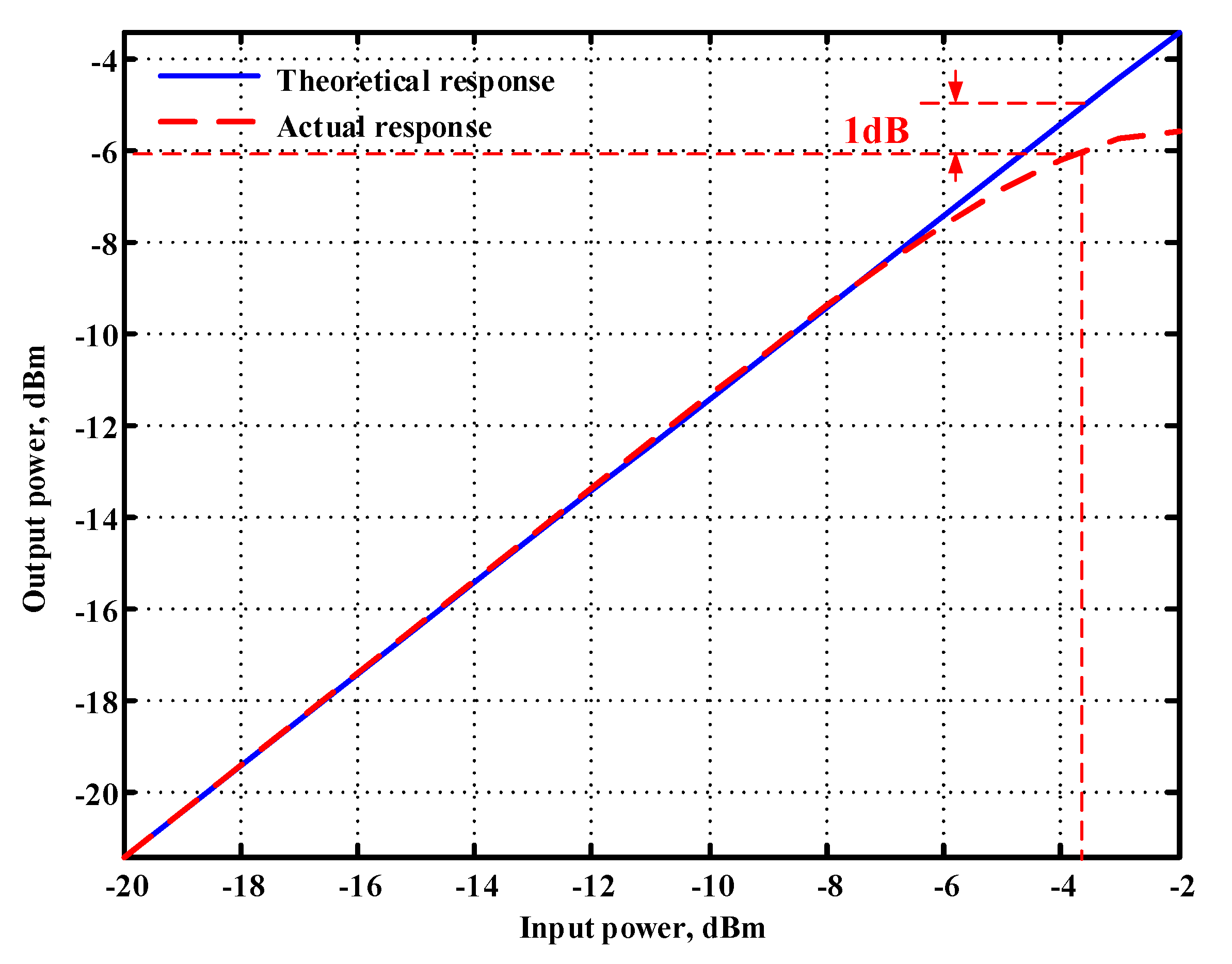
| Output P1dB (dBm) | N/A | N/A | N/A | N/A | N/A | N/A | −9.2 | −5.9 |
| Third-order IMD point | N/A | N/A | N/A | N/A | −37 dBc @ 35 mVp | N/A | −42.86 dBc @ 30 mVp | −48.67 dBc @ 63 mVp |
| Verification of simulation/experiment | yes/no | yes/no | yes/no | yes/no | yes/yes | yes/yes | yes/yes | yes/yes |
© 2020 by the authors. Licensee MDPI, Basel, Switzerland. This article is an open access article distributed under the terms and conditions of the Creative Commons Attribution (CC BY) license (http://creativecommons.org/licenses/by/4.0/).
Share and Cite
Wang, S.-F.; Chen, H.-P.; Ku, Y.; Lee, C.-L. Versatile Voltage-Mode Biquadratic Filter and Quadrature Oscillator Using Four OTAs and Two Grounded Capacitors. Electronics 2020, 9, 1493. https://doi.org/10.3390/electronics9091493
Wang S-F, Chen H-P, Ku Y, Lee C-L. Versatile Voltage-Mode Biquadratic Filter and Quadrature Oscillator Using Four OTAs and Two Grounded Capacitors. Electronics. 2020; 9(9):1493. https://doi.org/10.3390/electronics9091493
Chicago/Turabian StyleWang, San-Fu, Hua-Pin Chen, Yitsen Ku, and Chia-Ling Lee. 2020. "Versatile Voltage-Mode Biquadratic Filter and Quadrature Oscillator Using Four OTAs and Two Grounded Capacitors" Electronics 9, no. 9: 1493. https://doi.org/10.3390/electronics9091493
APA StyleWang, S.-F., Chen, H.-P., Ku, Y., & Lee, C.-L. (2020). Versatile Voltage-Mode Biquadratic Filter and Quadrature Oscillator Using Four OTAs and Two Grounded Capacitors. Electronics, 9(9), 1493. https://doi.org/10.3390/electronics9091493