Switching Characteristics and Mechanism Using Al2O3 Interfacial Layer in Al/Cu/GdOx/Al2O3/TiN Memristor
by
 and
and
Chiao-Fan Chiu
1,2, 
Sreekanth Ginnaram
3,
Asim Senapati
3,
Yi-Pin Chen
4 and
Siddheswar Maikap
3,4,* 1
Department of Pediatrics, Linkou Medical Center, Chang Gung Memorial Hospital, Taoyuan 33305, Taiwan
2
Graduate Institute of Clinical Medical Sciences, College of Medicine, Chang Gung University, Guishan, Taoyuan 33302, Taiwan
3
Thin Film Nano Tech. Lab., Department of Electronic Engineering, Chang Gung University, Taoyuan 33302, Taiwan
4
Department of Obstetrics and Gynecology, Keelung Chang Gung Memorial Hospital, Keelung 20401, Taiwan
*
Author to whom correspondence should be addressed.
Electronics 2020, 9(9), 1466; https://doi.org/10.3390/electronics9091466
Submission received: 19 July 2020
/
Revised: 20 August 2020
/
Accepted: 29 August 2020
/
Published: 7 September 2020
(This article belongs to the Special Issue Challenges and Applications of Non-volatile Memory)
Abstract
:Resistive switching characteristics by using the Al2O3 interfacial layer in an Al/Cu/GdOx/Al2O3/TiN memristor have been enhanced as compared to the Al/Cu/GdOx/TiN structure owing to the insertion of Al2O3 layer for the first time. Polycrystalline grain, chemical composition, and surface roughness of defective GdOx film have been investigated by transmission electron microscope (TEM), X-ray photoelectron spectroscopy (XPS), X-ray diffraction (XRD), and atomic force microscopy (AFM). For bipolar resistive switching (BRS) characteristics, the conduction mechanism of high resistance state (HRS) is a space-charge limited current for the Al/Cu/GdOx/TiN device while the Al/Cu/GdOx/Al2O3/TiN device shows Schottky emission. However, both devices show Ohmic at a low resistance state (LRS). After the device has been SET, the Cu filament evidences by both TEM and elemental mapping. Oxygen-rich at the Cu/GdOx interface and Al2O3 layer are confirmed by energy dispersive X-ray spectroscopy (EDS) line profile. The Al/Cu/GdOx/Al2O3/TiN memristor has lower RESET current, higher speed operation of 100 ns, long read pulse endurance of >109 cycles, good data retention, and the memristor with a large resistance ratio of >105 is operated at a low current of 1.5 µA. The complementary resistive switching (CRS) characteristics of the Al/Cu/GdOx/Al2O3/TiN memristor show also a low current operation as compared to the Al/Cu/GdOx/TiN device (300 µA vs. 3.1 mA). The transport mechanism is the Cu ion migration and it shows Ohmic at low field and hopping at high field regions. A larger hopping distance of 1.82 nm at the Cu/GdOx interface is obtained as compared to a hopping distance of 1.14 nm in the Al2O3 layer owing to a larger Cu filament length at the Cu/GdOx interface than the Al2O3 layer. Similarly, the CRS mechanism is explained by using the schematic model. The CRS characteristics show a stable state with long endurance of >1000 cycles at a pulse width of 1 µs owing to the insertion of Al2O3 interfacial layer in the Al/Cu/GdOx/Al2O3/TiN structure.
1. Introduction
Increasing demands on data storage in computing and mobile electronics are pushing the development of memories that continue to overcome the limits in scalability, storage-density, operation speed, and low power consumption [1,2]. Among several candidates of non-volatile memories, resistive random access memory (RRAM) has attracted much attention because of its potential to fulfill the above requirements [3,4,5,6]. Recently, cation migration based conductive bridging RAM [7,8] using several metal-oxides such as Al2O3 [9,10,11,12,13], Ta2O5 [12,14], SiO2 [15,16,17], HfO2 [18,19], Gd2O3 [20,21], ZrO2 [22], and LSMO [23,24] have been reported. However, unstable and inferior switching uniformity with a higher RESET current of a single switching layer needs to be improved for future practical application [20,21].
In order to mitigate those difficulties, the bi-layer concept has been introduced which leads to filament stability by controlling the Cu ion migration and reducing the RESET current [7,8,21,22]. Although there are numerous advantages of RRAM, the sneak path current is affecting its use in practical applications. To resolve the sneak path leakage current, the CRS concept has been introduced in which two BRS devices are anti-serially connected to one another [25,26]. Soni et al. [27] have reported the CRS characteristics in two anti-serially connected Pt/SiOx/Ge0.3Se0.7/Cu structures as well as in serially connected Pt/SiOx/Ge0.3Se0.7/Cu and Pt/Ge0.3Se0.7/SiOx/Cu structures. In our previous study [28], we have reported CRS characteristics using the IrOx/GdOx/Al2O3/TiN RRAM structure. Although there are some reports on BRS and CRS characteristics by using different structures [28,29], however, the Al2O3 interfacial layer in a Al/Cu/GdOx/Al2O3/TiN structure has been reported for the first time. A defective GdOx film [30] will be formed, which will easily help the migration of Cu ions under external bias and impact of inserting a thin Al2O3 layer leads to control of Cu ions migration owing to its lower ionic mobility [31]. Hence, insertion of Al2O3 interfacial layer in the Al/Cu/GdOx/Al2O3/TiN structure helps control the metallic filament formation/dissolution. This will also help reduce the operation current in BRS/CRS performance as compared to the single Al2O3 switching layer [13]. In this new structure, the GdOx is used as a Cu buffer layer, which easily helps the Cu filament forming/dissolving in the Al2O3 layer under low energy. As compared to other structures, this is very useful in the near future.
In this work, the BRS and CRS characteristics by using a new Al/Cu/GdOx/Al2O3/TiN device have improved performance as compared to the Al/Cu/GdOx/TiN devices. A small device size of 0.6 × 0.6 µm2 with a polycrystalline grain and defective GdOx films are confirmed by TEM, XPS, and XRD. The surface roughness of GdOx film is also observed by AFM. The Cu filament is observed by using high-resolution TEM (HRTEM) and EDS mapping. The CRS characteristics are also observed. The current conduction mechanism is also explained. By inserting a thin Al2O3 interfacial layer in the Al/Cu/GdOx/Al2O3/TiN memristor, this shows excellent BRS and CRS characteristics owing to control the Cu ion migration.
2. Materials and Methods
Memristor Fabrication Process
First, a 200 nm-thick SiO2 layer was grown by thermal oxidation on an 8-inch Si wafer. For a bottom electrode (BE), a 50 nm-thick TiN layer followed by a 150 nm-thick Ti was deposited on the SiO2/Si substrate. Then, a 150 nm-thick SiO2 as an insulating layer was deposited on the TiN/Ti/SiO2/Si stack. This SiO2 layer was the patterned via-holes. Then, a thin Al2O3 interfacial layer with a thickness of 2 nm was deposited on TiN BE by the rf sputtering process. The Al2O3 target with a purity of 99.9% was used. Next, the Gd2O3 layer with a thickness of approximately 17 nm was deposited. During deposition, some amount of oxygen was removed and the Gd2O3 film became GdOx (x < 1.5). In order to deposit a top electrode (TE), a Cu layer with a thickness of 40 nm and a 160 nm-thick Al as a capping layer were deposited in situ by thermal evaporation. Finally, the lift-off process was performed to obtain Al/Cu/GdOx/Al2O3/TiN (S2) memristors. The memory structure is shown by the sketch (Supplementary Information). For comparison, the Al/Cu/GdOx/TiN (S1) structure was also prepared without an Al2O3 interfacial layer. Microstructure, device size, and EDS mapping were observed by using the TEM-FEI Osiris system, which was operated at 200 kV. A crystalline Gd2O3 film was found by using the standard BRUKER XRD system with a Cu-kα source and wavelength was 1.541 Å. Non-stoichiometric GdOx and stoichiometric Al2O3 films were investigated by XPS with an Al (Kα) monochromatic X-ray and energy of 1486.6 eV was applied. The base vacuum pressure was 1 × 10⁻⁹ Torr. The crystalline film was confirmed by grazing incidence XRD (GIXRD), and the film was deposited on the Si substrate. AFM images were taken in tapping mode by using the Innova scanning probe microscope (AFM-SPM) system. Resistive switching characteristics were obtained by applying sweep voltage on the Al/Cu TE whereas the TIN BE was grounded. The electrical characterizations were performed by using both Agilent 4156C and B1500A semiconductor parameter analyzers.
3. Results and Discussion
3.1. Material Characteristics
3.1.1. TEM Image of Pristine Memristor
Figure 1a shows a typical TEM image of a S2 memristor. The device size is approximately 0.6 × 0.6 µm2. Figure 1b,c represents a high-resolution TEM image of inside and outside of the via-hole device, respectively. Each layer is observed clearly and thicknesses of the GdOx and Al2O3 layers are found to be 17 and 1.6 nm, respectively. The HRTEM image shows a polycrystalline GdOx film whereas an Al2O3 film shows amorphous. A clear crystallinity of GdOx film shows in the middle as compared to the GdOx/Cu interface and this interface shows a white color than the middle. This indicates that oxygen content at the Cu/GdOx interface is higher than the middle of the GdOx layer, which has been explained later. The inset of Figure 1c shows the Fast Fourier Transform (FFT) image of the GdOx film. The ring pattern of FFT indicates polycrystalline of the GdOx film. The d-spacing of highly intensive dots is calculated to be 3.11 Å, which represents the d-spacing value (3.06 Å) of Gd2O3 (100) plane [32].
3.1.2. XPS Analysis
The composition and chemical bonding of the GdOx/Al2O3 bilayers on the SiO2/Si substrate are analyzed by XPS spectra with their appropriate peak fitting (Figure 2). An XPS spectrum of Gd shows 3d3/2 and 3d5/2 doublet with a binding energy of 1220.5 and 1188.3 eV, respectively (not shown here), which correspond to the binding energy of Gd3d3/2 and 3d5/2 spin-orbits at 1218 and 1186 eV for the Gd2O3 film, respectively [33]. The XPS spectrum of Gd3d5/2 is shown in Figure 2a. The peak positions at 1188.71 and 1185.82 eV are identified to be Gd2O3 3d5/2 and metallic Gd3d5/2 peaks, respectively. The area ratio of Gd/Gd2O3 is approximately 0.69:1, which shows a higher percentage of Gd in the Gd2O3 film.
Figure 2b shows the O1s core-level spectra for the Gd2O3 films. This spectrum shows three distinct peaks. The strong peak at 531.6 eV corresponds to the oxygen in the Gd2O3 film, whereas lower and higher binding energy peaks at 529.4 eV (O1s B) and 532.9 eV (O1s A) are attributed to the hydroxyl and carbonate groups raised from the atmospheric exposure because of reactivity of Gd2O3 material [34,35]. Moreover, the lower binding energy peak at 529.4 eV can also correspond to the Gd-O bonding which indicates Gd-rich Gd2O3 [36]. On the other hand, oxygen can bind loosely with Gd on a polycrystalline grain or defective Gd2O3 switching material (SM), i.e., GdOx film. The Al2p and O1s peaks in Al2O3 layer are shown in Figure 2c,d, respectively. The Al2p and O1s peaks are located at 75.8 and 532.5 eV, respectively. This indicates a strong Al-O bonding with a stoichiometric Al2O3 interfacial layer.
3.1.3. XRD Pattern and AFM Image
In addition, the crystalline Gd2O3 film is confirmed by XRD pattern (Figure 3a). The peak at 28.7° (2θ) corresponds to (100) plane of Gd2O3 [31] whereas the peak at 55.02° (2θ) corresponds to (311) plane of Si [37]. This low intensity (100) peak is owing to the thin and defective (or oxygen vacancy) polycrystalline GdOx film. Figure 3b,c represents the AFM images on SiO2/Si and GdOx/Si substrates, respectively. The root-mean-square (Rq) and average (Ra) values of the GdOx films are found to be 0.688 and 0.518 nm, and those values are higher than the values of 0.321 and 0.257 nm for the SiO2 layer, respectively. This higher roughness of the GdOx films comes from the polycrystalline grains.
An explanation of higher defective GdOx film is as follows. During deposition of Al2O3, the film will contain some defects because of plasma. After Gd2O3 deposition on AlOx layer, the underneath layer took oxygen (O2−) from the Gd2O3 layer resulting in higher defective GdOx and stoichiometric Al2O3 layers that can be formed. In the case of the GdOx/Al2O3 bilayers, the Gd2O3 SM can be defective by two ways: (1) During deposition by electron beam evaporation and (2) oxygen consumption by the Al2O3 layer. Therefore, this higher defective GdOx layer or oxygen vacancy will easily help the migration of Cu ions whereas the Al2O3 layer will help in formation/dissolution of the filaments under an external electric field, which has a benefit for improvement of resistive switching memory characteristics as discussed later.
3.2. Bipolar Resistive Switching Characteristics
3.2.1. Current-Voltage Switching and Transport Mechanism
Bipolar current-voltage (I–V) characteristics and transport mechanism of the S1 and S2 memristors are shown in Figure 4. Typical forming voltages (Vform) are 2.4 and 2.1 V for the S1 and S2 devices, respectively (Figure 4a). However, the S2 devices have shown a lower and uniform Vform value as compared to the S1 devices (2.44 vs. 2.62 V at 50% probability) because of GdOx/Al2O3 bilayers (not shown here). Hundred devices for each structure have been measured randomly.
Typical bipolar I–V characteristics of the S1 and S2 devices after forming are shown in Figure 4b. The sweeping voltage direction is shown in arrow marks 1 to 4 (0→+2→0→−1→0 V). The SET voltage (VSET) is approximately 0.7 V. The S2 device has a lower RESET current (IRESET) than the S1 devices (630 µA vs. 2.85 mA), which is due to the Al2O3 interfacial layer. Similarly, the average IRESET value of S2 devices at 50% probability is approximately 540 µA from 100 devices (not shown here). Figure 4c depicts the cumulative probability of leakage current for both the S1 and S2 devices. It is known that the leakage current increases by decreasing the switching layer thickness or by increasing the number of defects [38]. Even though the GdOx/Al2O3 bilayer has a larger thickness of 19 nm than a single GdOx layer (17 nm), however, the S2 devices show a higher leakage current than the S1 devices (8.09 × 10⁻¹⁰ A vs. 3.05 × 10⁻¹¹ A at 50% probability). This is due to a higher defective GdOx as explained in XPS characteristics (Figure 2).
Considering the device-to-device distribution, the HRS/LRS values at 50% probability are 8.2/0.64 and 9.7/1.4 kΩ for the S1 and S2 devices, respectively. The LRS value of the S2 devices is higher than the S1 devices because of the smaller CF diameter. During formation, Cu atoms can be stored into the GdOx layer (or buffer layer) and a small diameter of conducting filament (CF) could be formed/dissolved in the Al2O3 layer under SET/RESET. However, transport mechanism is one of the key issues to understand the switching characteristics for both the devices as follows. For the S1 devices, the HRS currents for both positive and negative bias regions are plotted in a log-log scale (Figure 4d). The slope values are found to be 1.03–1.11 and 1.85–2.15, which have confirmed the space-charge-limited current (SCLC) conduction mechanism. Sun et al. [39] have also reported the SCLC conduction mechanism even if they have used the Au/CuO-DNA-Al/Au/Si structure. However, both S1 and S2 devices show Ohmic conduction at LRS currents.
To find the HRS current conduction, the HRS currents of the S2 devices are plotted in ln(J/T2) vs. √E (Figure 4e). The result is well fitted with Schottky emission (SE) at low field region [40]. By solving the equation of Schottky conduction, the dielectric constant (εSE) and barrier height (ΦB) are obtained as follows:
where kB is the Boltzmann’s constant, T is the absolute temperature, q is the electronic charge, and ε0 is the permittivity of free space, S is the slope, and I is the intercept of linear plot in ln(J/T2) vs. √E plot. However, an interesting point to be noted is that when we consider the pristine device thickness, i.e., approximately 19 nm the obtained εSE value is quite low approximately 2. This does not follow the εSE = n2 (n = refractive index) relation because the reported n value of GdOx film is <2 within the visible wavelength [41]. If we consider the effective thickness 7.5 nm (dissolution gap after RESET) then the εSE value becomes approximately 3.9, which is within the considerable range and follows the εSE = n2. This conflict signifies that after the RESET process some of the Cu atoms accumulate inside the GdOx switching material and reduce the effective thickness of dissolution gap. From Equations (1) and (2), the corresponding ΦB value at HRS is approximately 0.48 eV.
By considering electron affinities of GdOx (2.05 eV [42]) and Al2O3 (1 eV [43]), energy gaps of GdOx (5.4 eV [41]) and Al2O3 (7.1 eV [44]), and work functions of Cu (4.46 eV [45] and TiN (4.6 eV [46]), the energy bands are shown in dotted lines under thermal equilibrium at 300 K (Figure 4f). To emit the electron, it is found that the barrier height at the Al2O3/TiN interface is higher than the GdOx/Cu interface (2.5 vs. 0.94 eV). Under a positive bias on the Cu TE, the energy gap of GdOx is reduced owing to the Cu migration. After RESET, a dissolution gap at the GdOx/Al2O3 interface and the Al2O3 layer is observed, which represents the HRS. Then, Schottky emission is obtained under a positive bias before SET because the electron conducts from the TiN BE and crosses the Al2O3 conduction barrier. Furthermore, we can speculate that the filament formation-and dissolution is controlled by the Al2O3 interfacial layer. However, the Cu ion migration under an external field is responsible to change HRS to LRS or vice versa, which has been evidenced below.
3.2.2. Evidence of Cu Migration
To find an evidence of Cu ion migration under SET, the S2 memristor with a typical size of 0.6 × 0.6 µm2 switches with two consecutive cycles at a high CC of 10 mA. After that, this device was kept at LRS and the device was used for TEM observation, elemental depth profile, and EDS mapping (Figure 5). All layers are observed (Figure 5a), which are seen in a fresh device (Figure 1), except a Cu filament in the GdOx/Al2O3 bilayers. Figure 5b shows the HRTEM image, where a few nanometer size of the dark spots (or Cu filament) are clearly observed in the marked region. To know the elemental composition with and without Cu filament regions, the same device is characterized by the scanning transmission electron microscope (STEM) and corresponding images are shown in Figure 5c,d. The EDS depth profiles with and without Cu filament regions are shown in Figure 5e,f, respectively. The EDS line scans of Ti, N, Gd, O, Al, and Cu elements are taken from the Ti BE to Al capping layer, as shown with arrows in Figure 5c,d.
From the EDS depth profiles of nitrogen (Figure 5f), it is found that the TiN layer with a thickness of approximately 30 nm is shown on Ti. The thickness of GdOx layer is approximately 17 nm. A low atomic concentration (5.5%) of the Al peaks at the GdOx/TiN interface is observed because of a thin (2 nm) Al2O3 interfacial layer. It is interesting to note that the atomic concentration of O at the TiN BE/GdOx interface is higher than the value at the GdOx/Cu TE interface (20.3 vs. 13.2%), which indicates the oxygen consumption at the Al2O3 interfacial layer. Therefore, the Gd2O3 layer becomes more defective, which is consistent with XPS results (Figure 2). The EDS line scan profile along the Cu filament is marked at four positions 1, 2, 3, and 4, as shown in Figure 5c,e. The sequence 1, 2, 3, and 4 positions indicates the TiN, Al2O3, GdOx, and GdOx/Cu interface layers, respectively. The elemental concentrations of Gd at positions 1, 2, 3, and 4 are 6.5, 11.6, 36.9, and 19.3%, while those values of Cu are 29, 57.5, 16, and 41.9%, respectively. A large amount of Cu at position 2 is diffused into the TiN electrode owing to the high CC of 10 mA. It is noted that this observation is reported for the first time. This suggests that joule heating may help diffuse Cu into TiN. At position 1, a small amount of Gd appears, which is originated during Cu migration. A small amount of Cu at position 3 is observed, which suggests a neck of this CF. Some amount of Cu at position 4 is observed, where Cu starts to diffuse or this position demonstrates that the CF is formed during the SET operation at the GdOx/Cu interface.
EDS elemental mappings of Al, Cu, Gd, O, Ti, and N elements are shown in Figure 5g–l. All elements in these layers are observed clearly. In Figure 5h, the Cu elemental mapping represents a beautiful Cu filament. Thanks to the Cu migration mechanism for real non-volatile memory applications. A hump-like shape of Cu at the Cu/GdOx interface is observed under the SET operation, which initiates the formation of CF.
Figure 6a shows the HRTEM image of Cu/GdOx interface without the Cu filament region. The inset in Figure 6a shows the FFT image of marked region. The d-spacing values from the FFT image are found to be d1 = 1.99 Å, d2 = 3.08 Å, and d3 = 3.91 Å. The value of 1.99 Å is much closer to the reported value (2.088 Å) of Cu (111) plane [47]. However, values of 3.08 and 3.91 Å are higher due to overlapping of two Cu crystals, where the d-spacing of moire’ fringes is increased [48]. As further investigation of Cu diffusion in TiN BE we have analyzed the HRTEM, as shown in Figure 6b. The Cu filament region is marked as a conical shape with a dotted line. We can clearly observe the diffused Cu in the TiN BE.
The mass percentage values from the EDS depth profile (Figure 5e) of Ti and N are approximately 50 and 20, respectively, which shows non-stoichiometric TiNx (x < 1). Under the high current, this TiNx BE can allow the Cu diffusion through grain boundaries or defects. Olowolafe et al. [49] have reported the diffusion of Cu through the TiNx layer at high temperatures in the Cu/TiNx/Si structure. Mühlbacher et al. [50] have reported Cu diffusion in a single crystalline TiN layer at high temperatures. Wu et al. also reported the diffusion of Ni in Ni/HfO2/SiO2/Si [51] and NiSi/HfO2/SiO2/Si [52] structures. The d-spacing value in TiN BE is 2.71 Å, which is similar to the reported value (2.45 Å) of TiN (111) plane [53]. The d-spacing value in the Cu filament region is large 5.43 Å owing to the moire’ fringes because diffused Cu crystals and TiN (111) plane are overlapped. To understand the moiré fringes of diffused Cu in TiN, a further study needs to continue in future.
Other researchers have reported the Cu or Ag migration in different oxide or solid-electrolyte materials [54,55]. The CF with nanocrystals (NCs) are also reported in the Ag/a-Si/Pt structure by Yang et al. [54] and Cu protrusion in Cu/HfO2/Pt devices is observed by Lv et al. [19]. Vianello et al. [55] have shown the evidence of the Ag filament using the Ag/Sb-doped GeS2/W structure. Liu et al. have observed the localized and controllable Ag nano-filament growth in the Ag/ZrO2/Cu NC/Pt structure by using an in situ TEM technique [56]. The Cu NC was decorated on Pt BE. The superior uniformity of resistive switching properties is obtained, which is owing to enhance and concentrate the electric field on Cu NC sites. This will control the location and orientation of the Ag CFs. On the other hand, the Ag nano-filament is formed by a mass transfer from Ag nano clusters in the Au nano-tip/SiO2/Ag NC/p-Si structure [16]. The discrete CF is observed by in situ TEM. However, proper decoration of nanocrystals/clusters on the nanoscale device is one of the critical tasks. Yuan et al. have reported the Cu tip size dependent CF nature in the Cu tip/SiO2/W structure by an in situ TEM [57]. For a smaller Cu tip size, the CF shows as thin and in the shape of discrete clusters owing to the limited ion supply. On the other hand, a wide CF in continuous is observed for the larger Cu tip owing to sufficient ion injection and lower surface energy. This suggests that the discrete CF under nano-ampere operation may be not sufficient for a reliable non-volatile memory application. Further investigation is still needed of nano-ionic memristive switching dynamics at higher resolution and dimensions for experimental study [58,59]. The switching mechanism evolution in greater resolution is a key part for the real non-volatile memory and memory in computing applications. In our study, it is possible to say that the Cu filament formation/dissolution in the Al2O3 interfacial layer, which is observed by ex situ HRTEM, will control the resistive switching performance. This has been discussed below.
3.2.3. Device Performance and Low Current Operation
Figure 7a represents program/erase (P/E) endurance of the S1 and S2 devices with a high-speed operation. The P/E voltage and pulse width are applied +1.5 V/−0.8V and 100 ns/1 µs, respectively. The S2 devices show longer P/E cycles as compared to the S1 devices. After a few P/E cycles (~30), the S1 devices show failure because of uncontrolled Cu migration whereas the Cu filament formation/dissolution is controlled by the Al2O3 interfacial layer. Figure 7b shows read pulse endurance of the S1 and S2 devices with a small pulse width of 1 µs. The S1 devices show failure after 5 × 10⁸ cycles whereas the S2 devices show a long read endurance of >109 cycles even at low current operation of 100 µA. The values of HRS/LRS are approximately 27/260 Ω and 348/379 Ω for the S1 and S2 devices at CC of 500 µA, respectively. The S2 device shows higher resistance ratio of 900 than the value of 100 for the S1 devices owing to the narrower Cu filament formation/dissolution in the Al2O3 layer. The HRS (~259 kΩ) and LRS (~1.57 kΩ) of the S2 devices at a CC of 100 µA also show good stability with a resistance ratio of >150. Figure 7c represents a stable data retention of about 20,000 s of our S2 memory device at CC of 100 µA.
Figure 7d shows typical bipolar resistive switching (BRS) characteristics of the S2 devices under at a very low CC of 1.5 µA. A high resistance ratio of >105 at a Vread of 0.5 V is achieved, even a low RESET current of <1 nA is observed. Therefore, the S2 device can have a high speed (100 ns) and low current operation of 1.5 µA. Further, the S2 devices has the possibility to exhibit a multi-level cell operation. However, proper controlling of the operation voltage of these devices will have complementary resistive switching (CRS) characteristics in a single cell, which have been reported for the first time in this study below.
3.3. CRS Phenomena
3.3.1. I–V and Transport Characteristics
Although there are numerous advantages of BRS memory, the sneak path current is affecting its use in practical three-dimensional (3D) cross-point applications. Recently, the CRS phenomena has been proposed to resolve the sneak path effect by using two anti-serially cells [25,26]. In our study, both S1 and S2 memristors show CRS characteristics after adjusting the sweeping voltage (Figure 8). The voltage sweeping direction is indicated by arrow 1–2. The resistance states are denoted as “0”, “ON” and “1”, respectively.
The electroforming process is applied under a negative bias for both pristine S1 and S2 memristors. The values of VSET1, VSET2, VRESET1, and VRESET2 for the S1 devices (Figure 8a) are found to be 0.88, −0.88, −1.4, and 1.3 V, while those values are found to be 0.78, −0.76, −1.3, and 1.1 V for the S2 devices (Figure 8b), respectively. Both devices have been operated under a low voltage of ±1.5 V. However, the operation current (~300 µA) of the S2 devices is about 11 times lower than that of the S1 devices (3.1 mA), which is very useful for low power operation of the cross-point memory arrays. Therefore, the Al2O3 layer has been beneficial.
To understand the current transport characteristics, the I–V curves of the S2 devices are fitted, as shown in Figure 8c,d. Both “0” and “1” states at low field of negative and positive bias regions confirm the Ohmic conduction with slope values from 1.06 to 1.15. The high field region is plotted in ln(J) vs. E for the hopping conduction [28], which is expressed below:
where Jhopping is the current density due to the hopping conduction, ‘a’ is the mean hopping distance, n is the electron concentration in the conduction band of dielectric, v is the frequency of thermal vibration of electrons at trap sites, and Ea is the activation energy. From Equation (4), we have obtained an equation for hopping distance (a) below:
where S is the slope. By using Equation (4), the hopping distance values for both “0” state at a positive bias and “1” state at a negative bias are found to be 1.80 and 1.82 nm (Figure 8c), while those values for both “0” state at a negative bias and “1” state at a positive bias are found to be 1.14 and 1.41 nm (Figure 8d), respectively. Yan et al. [60] have also reported the hopping distance of approximately 2 nm by using the TiW/Cu2O/Cu structure. Figure 8e shows read stable endurance of 1000 cycles with a small pulse width of 1 µs. The “ON” state and “1” state are read at a Vread of −1 V, whereas the “0” state is read at a 1/2Vread of −0.5 V. The non-linearity factor is approximately 6, which is useful for 3D cross-point arrays in the near future.
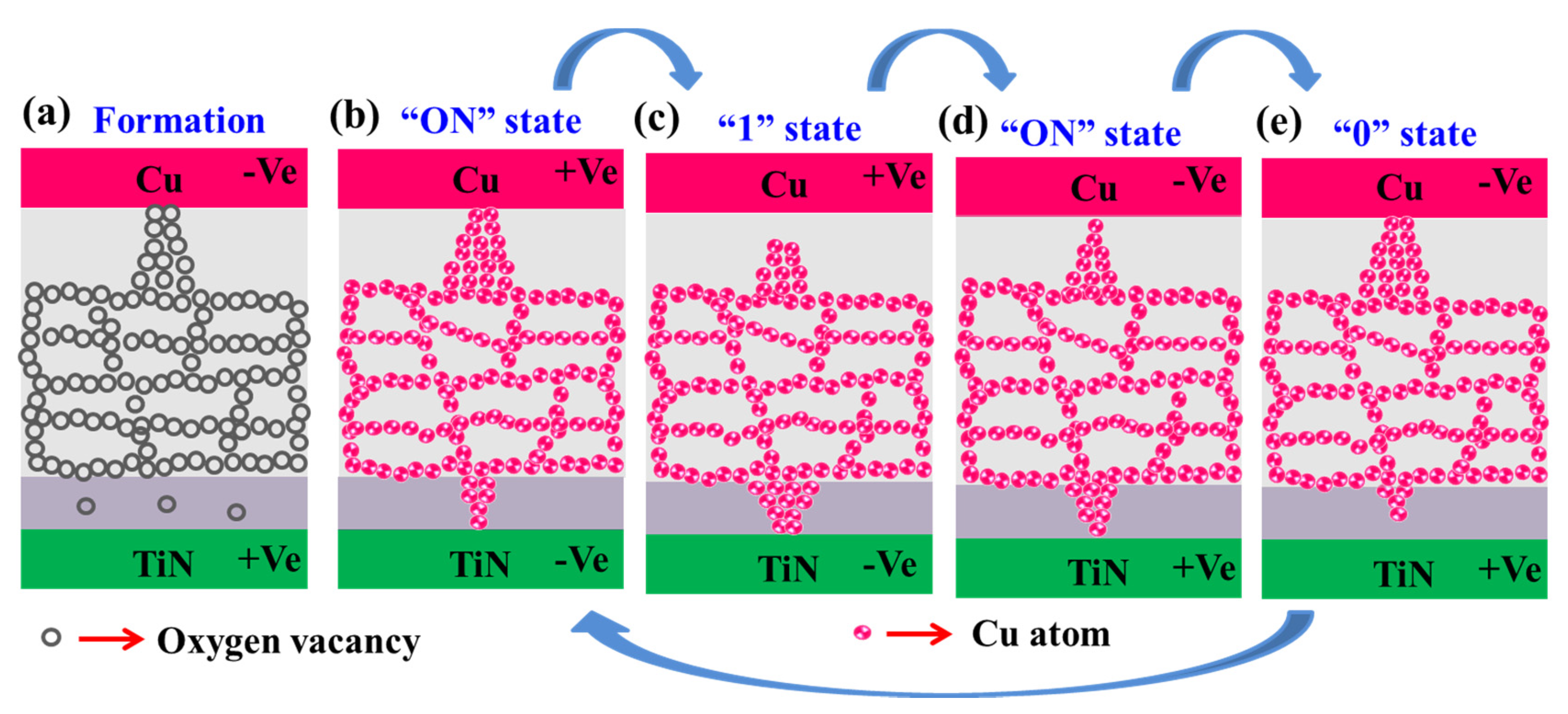
3.3.2. Memristor Mechanism
The switching mechanism of the CRS characteristics is demonstrated schematically in Figure 9. From this model, the CRS depends on Cu ions’ migration through the GdOx/Al2O3 bilayer. Initially, both the Al2O3 layer and GdOx/Cu TE interface are less defective than GdOx layer, as we can see from the oxygen-rich layer (Figure 5f). When a negative bias is applied on the Cu TE, Gd-O bonds at grain boundary break easily and O2− ions are migrated towards the GdOx/TiN interface. On the other hand, O2− ions are accumulated at the Cu/GdOx interface because of the inert Cu electrode or repel O2− ions by Cu electrode, which results in oxygen vacancy filament formation at the Cu/GdOx interface (Figure 9a).
When a positive voltage is applied on the Cu TE (>VSET1), the Cu ions are generated by oxidation method (Cu° → Cuz+ + ze−, z = 1, 2) [5] and these Cu ions migrate towards the Al2O3/TiN interface through oxygen vacancy under an electric field as well as a Cu filament can be formed in the Al2O3 layer and current increases (Figure 9b). Due to more oxygen vacancies in the GdOx grain boundaries, the Cu ions arrange accordingly and those neutralize by taking the electron from the BE through reduction process (Cuz+ + ze− → Cu°). At VSET1, the “0” state changes to “ON” state. Further increment of a positive voltage up to 1 V leads to a larger filament diameter in the Al2O3 layer. However, if the positive voltage is more than 1 V then the electric field is developed across the Cu/GdOx interface and the filament is dissolved (Figure 9c). Maximum dissolution of the filament is observed up to VRESET2 and the “ON” state changes to “1” state of “OFF” state.
Similarly, when a negative voltage (<VSET2) is applied on the TE, the Cu ions migrate towards the Cu/GdOx interface from GdOx grain boundaries and the Cu filament is formed at the Cu/GdOx interface as current increases (Figure 9d). The “1” state changes to “ON” state. By decreasing the negative voltage up to −1.06 V the filament diameter is becoming thicker at the Cu/GdOx interface. If the negative voltage is less than −1.06 V the dissolution of filament is started in the Al2O3 layer and it has a maximum dissolution up to VRESET1 as well as “ON” state changes to “0” state or “OFF” state (Figure 9e). In our study, we did not fabricate the back to back memristor structure. Two cells are the Cu/GdOx interface and Al2O3 layer where the Cu incorporated GdOx layer is a virtual common electrode in a single Al/Cu/GdOx/Al2O3/TiN memristor, which is equivalent to the back to back memristor structure. The Cu filament formation/dissolution happens at the Cu/GdOx interface and Al2O3 layer alternately by optimizing the RESET voltage and the CRS mechanism explained as well.
Similarly, the CRS mechanism of the Al/Cu/GdOx/TiN structure can be explained because of TiNxOy layer formation at the GdOx/TiN interface during a negative bias applied on the pristine device (Figure 8a). From Figure 8, it is observed that the Cu ions are transported by hopping. The hopping distance at the Cu/GdOx interface is higher than the Al2O3 layer (1.80 to 1.82 nm vs. 1.14 to 1.41 nm). Therefore, the filament length at the Cu/GdOx interface is longer than the Al2O3 layer. These CRS characteristics show a stable and long endurance of >1000 cycles and are promising for next generation 3D cross-point memory applications.
4. Conclusions
Improved BRS and CRS characteristics of the Al/Cu/GdOx/Al2O3/TiN memristors have been reported as compared to the Al/Cu/GdOx/TiN devices, for the first time, owing to insertion of Al2O3 interfacial layer. The defective polycrystalline grain and composition of the GdOx film are observed by TEM, XPS, and XRD. The Al/Cu/GdOx/Al2O3/TiN devices show stable BRS characteristics with lower RESET current, stable P/E endurance with a high speed of 100 ns, long read endurance of >109 cycles with a pulse width of 1 µs, good data retention, and good device-to-device uniformity. This is due to the Cu filament formation/dissolution in the Al2O3 interfacial layer under external bias, which evidences by TEM, EDS elemental mapping, and line scan. The S1 device shows SCLC while the S2 device shows Schottky emission with a barrier height of 0.48 eV. However, both devices show Ohmic conduction at LRS. The S2 devices can be operated at low current of 1.5 µA with a large resistance ration of >105, which is very useful for a multi-level operation with low power non-volatile memory applications.
It is found that the CRS characteristics of the S2 memristor are observed at low current operation as compared to the S1 (300 µA vs. 3.1 mA) because insertion of the Al2O3 layer has been beneficial. Transport mechanism of the CRS characteristics is Ohmic at low field and hopping conduction at high field regions. The hopping distance of Cu ion migration is 1.82 nm at the Cu/GdOx interface while it is 1.14 nm in the Al2O3 layer. The CRS characteristics have been explained by using the schematic model. Therefore, the Al/Cu/GdOx/Al2O3/TiN memristor is very useful in the future 3D cross-point memory architecture. This memristor can be extended to an artificial synapse, bio-sensing with a Cu reduction-oxidation mechanism, as well as artificial intelligence (AI) in the future.
Supplementary Materials
The following are available online at https://www.mdpi.com/2079-9292/9/9/1466/s1.
Author Contributions
Both C.-F.C. and S.G. wrote the first draft under instruction of S.M.; S.G. measured the memristors; both C.-F.C. and A.S. analyzed and modified the manuscript; Y.-P.C. suggested and discussed to modify the manuscript; S.M. finalized the manuscript. All authors have read and agreed to the published version of the manuscript.
Funding
Ministry of Science and Technology (MOST) Taiwan, under contract numbers: MOST-107-2221-E-182-041 and MOST-108-2221-E-182-026.
Acknowledgments
The authors are grateful to the Ministry of Science and Technology (MOST) Taiwan, under contract numbers: NSC-102-2221-E-182-057-MY2, MOST-107-2221-E-182-041, and MOST-108-2221-E-182-026. The authors are also grateful to MSSCORPS CO., LTD., Hsinchu, Taiwan for their support on TEM, EDS mapping, and EDS depth profile.
Conflicts of Interest
The authors declare no conflict of interest.
References
- Banerjee, W. Challenges and applications of emerging nonvolatile memory devices. Electronics 2020, 9, 1029. [Google Scholar] [CrossRef]
- Slesazeck, S.; Mikolajick, T. Nanoscale resistive switching memory devices: A review. Nanotechnology 2019, 30, 352003. [Google Scholar] [CrossRef]
- Waser, R.; Aono, M. Nanoionics-based resistive switching memories. Nat. Mater. 2007, 6, 833–840. [Google Scholar] [CrossRef] [PubMed]
- Pan, F.; Gao, S.; Chen, C.; Song, C.; Zeng, F. Recent progress in resistive random access memories: Materials, switching mechanisms, and performance. Mater. Sci. Eng. R Rep. 2014, 83, 1–59. [Google Scholar] [CrossRef]
- Jana, D.; Roy, S.; Panja, R.; Dutta, M.; Rahaman, S.Z.; Mahapatra, R.; Maikap, S. Conductive-bridging random access memory: Challenges and opportunity for 3D architecture. Nanoscale Res. Lett. 2015, 10, 188. [Google Scholar] [CrossRef] [PubMed] [Green Version]
- Maikap, S.; Banerjee, W. In quest of nonfilamentary switching: A synergistic approach of dual nanostructure engineering to improve the variability and reliability of resistive random-access-memory devices. Adv. Electron. Mater. 2020, 6, 2000209. [Google Scholar] [CrossRef]
- Dutta, M.; Maikap, S.; Qiu, J.T. Controlling conductive filament and tributyrin sensing using an optimized porous iridium interfacial layer in Cu/Ir/TiNxOy/TiN. Adv. Electron. Mater. 2019, 5, 1800288. [Google Scholar]
- Ginnaram, S.; Qiu, J.T.; Maikap, S. Role of the Hf/Si interfacial layer on the high performance of MoS2-basedconductive bridge RAM for artificial synapse application. IEEE Electron Device Lett. 2020, 41, 709–712. [Google Scholar] [CrossRef]
- Senapati, A.; Roy, S.; Lin, Y.-F.; Dutta, M.; Maikap, S. Oxide-electrolyte thickness dependence diode-like threshold switching and high on/off ratio characteristics by using Al2O3 based CBRAM. Electronics 2020, 9, 1106. [Google Scholar] [CrossRef]
- Belmonte, A.; Radhakrishnan, J.; Goux, L.; Donadio, G.L.; Kumbhare, P.; Redolfi, A.; Delhougne, R.; Nyns, L.; Devulder, W.; Witters, T.; et al. Co active electrode enhance CBRAM and scaling potential. In Proceedings of the IEEE International Electron Devices Meeting 2019, San Francisco, CA, USA, 7–11 December 2019. [Google Scholar]
- Kim, S.M.; Kim, H.J.; Jung, H.J.; Kim, S.H.; Park, J.Y.; Seok, T.J.; Park, T.J.; Lee, S.W. Highly uniform resistive switching performances using two-dimensional electron gas at a thin-film heterostructure for conductive bridge random access memory. ACS Appl. Mater. Interfaces 2019, 11, 30028–30036. [Google Scholar] [CrossRef]
- Roy, S.; Maikap, S.; Sreekanth, G.; Dutta, M.; Jana, D.; Chen, Y.Y.; Yang, J.R. Improved resistive switching phenomena and mechanism using Cu-Al alloy in a new Cu:AlOx/TaOx/TiN structure. J. Alloys Compd. 2015, 637, 517–523. [Google Scholar] [CrossRef]
- Hubbard, A.W.; Kerelsky, A.; Jasmin, G.; White, E.R.; Lodico, J.; Mecklenburg, M.; Regan, B.C. Nanofilament formation and regeneration during Cu/Al2O3 resistive memory switching. Nano Lett. 2015, 15, 3983–3987. [Google Scholar] [CrossRef] [PubMed] [Green Version]
- Banno, N.; Sakamoto, T.; Iguchi, N.; Sunamura, H.; Terabe, K.; Hasegawa, T.; Aono, M. Diffusivity of Cu ions in solid electrolyte and its effect on the performance of nanometer-scale switch. IEEE Trans. Electron Devices 2008, 55, 3283–3287. [Google Scholar] [CrossRef]
- Schindler, C.; Thermadam, S.C.P.; Waser, R.; Kozicki, M.N. Bipolar and unipolar resistive switching in Cu-doped SiO2. IEEE Trans Electron Devices 2007, 54, 2762–2768. [Google Scholar] [CrossRef]
- Tian, X.; Wang, L.; Wei, J.; Yang, S.; Wang, W.; Xu, Z.; Bai, X. Filament growth dynamics in solid electrolyte-based resistive memories revealed by in situ TEM. Nano Res. 2014, 7, 1065–1072. [Google Scholar] [CrossRef]
- Liu, C.Y.; Huang, J.J.; Lai, C.H.; Lin, C.H. Influence of embedding Cu nano-particles into a Cu/SiO2/Pt structure on its resistive switching. Nanoscale Res. Lett. 2013, 8, 156–166. [Google Scholar] [CrossRef] [PubMed] [Green Version]
- Zhao, X.; Liu, S.; Niu, J.; Liao, L.; Liu, Q.; Xiao, X.; Lv, H.; Long, S.; Banerjee, W.; Li, W.; et al. Confining cation injection to enhance CBRAM performance by nanopore graphene layer. Small 2017, 13, 1603948. [Google Scholar] [CrossRef]
- Lv, H.; Xu, X.; Liu, H.; Liu, R.; Liu, Q.; Banerjee, W.; Sun, H.; Long, S.; Li, L.; Liu, M. Evolution of conductive filament and its impact on reliability issues in oxide-electrolyte based resistive random access memory. Sci. Rep. 2015, 5, 1–6. [Google Scholar] [CrossRef]
- Aratani, K.; Ohba, K.; Mizuguchi, T.; Yasuda, S.; Shiimoto, T.; Tsushima, T.; Sone, T.; Endo, K.; Kouchiyama, A.; Sasaki, S.; et al. A novel resistance memory with high scalability and nanosecond switching. In Proceedings of the 2007 IEEE International Electron Devices Meeting, Washington, DC, USA, 10–12 December 2007. [Google Scholar]
- Zhao, H.; Tu, H.; Wei, F.; Shi, Z.; Xiong, Y.; Zhang, Y.; Du, J. High mechanical endurance RRAM based on amorphous gadolinium oxide for flexible nonvolatile memory application. J. Phys. D Appl. Phys. 2015, 48, 205104. [Google Scholar] [CrossRef]
- Wu, F.; Si, S.; Cao, P.; Wei, W.; Zhao, X.; Shi, T.; Zhang, X.; Ma, J.; Cao, R.; Liao, L.; et al. Interface engineering via MoS2 insertion layer for improving resistive switching of conductive-bridging random access memory. Adv. Electron. Mater. 2019, 5, 18747. [Google Scholar] [CrossRef]
- Liu, D.; Cheng, H.; Zhu, X.; Wang, G.; Wang, N. Analog memristors based on thickening/thinning of Ag nanofilaments in amorphous manganite thin films. ACS Appl. Mater. Interfaces 2013, 5, 11258–11264. [Google Scholar] [CrossRef] [PubMed]
- Liu, D.; Wang, N.; Wang, G.; Shao, Z.; Zhu, X.; Zhang, C.; Cheng, H. Programmable metallization cells based on amorphous La0.79Sr0.21MnO3 thin films for memory applications. J. Alloys Compd. 2013, 580, 354–357. [Google Scholar] [CrossRef]
- Xu, R.; Jang, H.; Lee, M.-H.; Amanov, D.; Cho, Y.; Kim, H.; Park, S.; Shin, H.-J.; Ham, D. Vertical MoS2 double-layer memristor with electrochemical metallization as an atomic-scale synapse with switching thresholds approaching 100 mV. Nano Lett. 2019, 19, 2411–2417. [Google Scholar] [CrossRef] [PubMed]
- Linn, E.; Rosezin, R.; Kügeler, C.; Waser, R. Complementary resistive switches for passive nanocrossbar memories. Nat. Mater. 2010, 9, 403–406. [Google Scholar] [CrossRef]
- Soni, R.; Meuffels, P.; Petraru, A.; Hansen, M.; Ziegler, M.; Vavra, O.; Kohlstedt, H.; Jeong, D.S. Bipolar switching polarity reversal by electrolyte layer sequence in electrochemical metallization cells with dual-layer solid electrolytes. Nanoscale 2013, 5, 12598–12606. [Google Scholar] [CrossRef]
- Jana, D.; Samanta, S.; Maikap, S.; Cheng, H.M. Evolution of complementary resistive switching characteristics using IrOx/GdOx/Al2O3/TiN structure. Appl. Phys. Lett. 2016, 108, 011605. [Google Scholar] [CrossRef] [Green Version]
- Qiu, J.T.; Samanta, S.; Dutta, M.; Ginnaram, S.; Maikap, S. Controlling resistive switching by using an optimized MoS2 interfacial layer and the role of top electrodes on ascorbic acid sensing in TaOx-based RRAM. Langmuir 2019, 35, 3897–3906. [Google Scholar] [CrossRef]
- Cao, X.; Li, X.; Gao, X.; Yu, W.; Liu, X.; Zhang, Y.; Chen, L.; Cheng, X. Forming-free colossal resistive switching effect in rare-earth oxide Gd2O3 films for memristor application. J. Appl. Phys. 2009, 106, 073723. [Google Scholar] [CrossRef] [Green Version]
- Sakamoto, T.; Banno, N.; Iguchi, N.; Kawaura, H.; Sunamura, H.; Fujieda, S.; Terabe, K.; Hasegawa, T.; Aono, M. A Ta2O5 solid-electrolyte switch with improved reliability. In Proceedings of the 2007 IEEE Symposium on VLSI Technology, Kyoto, Japan, 12–14 June 2007. [Google Scholar]
- Cho, H.K.; Cho, H.J.; Lone, S.; Kim, D.D.; Yeum, J.H.; Cheong, I.W. Preparation and characterization of MRI-active gadolinium nano composite particles for neutron capture therapy. J Mater. Chem. 2011, 21, 15486. [Google Scholar] [CrossRef]
- Ahren, M.; Selegard, L.; Klasson, A.; Soderlind, F.; Abrikossova, N.; Skoglund, C.; Bengtsson, T.; Engstrom, M.; Kall, P.O.; Uvda, K. Synthesis and characterization of PEGylated Gd2O3 nanoparticles for MRI contrast enhancement. Langmuir 2010, 26, 5753–5762. [Google Scholar] [CrossRef]
- Majeeda, S.; Shivashankar, S.A. Rapid microwave-assisted synthesis of Gd2O3 and Eu:Gd2O3 nanocrystals: Characterization, magnetic, optical and biological studies. J. Mater. Chem. B 2014, 2, 5585–5593. [Google Scholar] [CrossRef] [PubMed]
- Khan, S.A.; Gambhir, S.; Ahmad, A. Extracellular biosynthesis of gadolinium oxide (Gd2O3) nanoparticles, their biodistribution and bioconjugation with the chemically modified anticancer drug taxol. Beilstein J. Nanotechnol. 2014, 5, 249–257. [Google Scholar] [CrossRef] [PubMed] [Green Version]
- Dawei, Y.; Hong, Z.; Li, B.; Xuemin, W.; Weibin, Z.; Yuying, W.; Changle, S.; Liping, P.; Weidong, W. Thickness dependence of the initial oxidation behaviors of Gd films grown on Si by laser molecular beam epitaxy. J. Wuhan Univ. Technol. Mater. Sci. Ed. 2012, 27, 191–194. [Google Scholar]
- Li, N.; Chen, N.; Bai, Y.; He, H. Preparation and properties of polycrystalline silicon seed layers on graphite substrate. J. Semicond. 2012, 33, 113003. [Google Scholar] [CrossRef]
- Yang, K.J.; Hu, C. MOS capacitance measurements for high leakage thin dielectrics. IEEE Trans. Electron Dev. 1999, 46, 1500–1501. [Google Scholar] [CrossRef] [Green Version]
- Sun, B.; Wei, L.; Li, H.; Jia, X.; Wu, J.; Chen, P. The DNA strand assisted conductive filament mechanism for improved resistive switching memory. J. Mater. Chem. C 2015, 3, 12149–12155. [Google Scholar] [CrossRef]
- Dutta, M.; Senapati, A.; Ginnaram, S.; Maikap, S. Resistive switching memory and artificial synapse by using Ti/MoS2 based conductive bridging cross-points. Vacuum 2020, 176, 109326. [Google Scholar] [CrossRef]
- Ferrara, M.C.; Altamura, D.; Schioppa, M.; Tapfer, L.; Nichelatti, E.; Pilloni, L.; Montecchi, M. Growth, characterization and optical properties of nanocrystalline gadolinia thin films prepared by sol–gel dip coating. J. Phys. D Appl. Phys. 2008, 41, 225408. [Google Scholar] [CrossRef]
- Lipp, E.; Shahar, Z.; Bittel, B.C.; Lenahan, P.M.; Osten, H.J.; Eigenberg, M. Trap assisted conduction in Pt-gated Gd2O3/Si capacitors. J. Appl. Phys. 2011, 109, 073724. [Google Scholar] [CrossRef]
- Robertson, J.; Falabretti, B. Band offsets of high k gate oxides on III-V semiconductors. J. Appl. Phys. 2006, 100, 014111. [Google Scholar] [CrossRef]
- Filatova, E.O.; Konashuk, A.S. Interpretation of the changing the band Gap of Al2O3 depending on its crystalline form: Connection with different local symmetries. J. Phys. Chem. C 2015, 119, 20755–20761. [Google Scholar] [CrossRef]
- Rahaman, S.Z.; Maikap, S.; Das, A.; Prakash, A.; Wu, Y.H.; Lai, C.S.; Tien, T.C.; Chen, W.S.; Lee, H.-Y.; Chen, F.T.; et al. Enhanced nanoscale resistive switching memory characteristics and switching mechanism using high-Ge-content Ge0.5Se0.5 solid electrolyte. Nanoscale Res. Lett. 2012, 7, 614. [Google Scholar] [CrossRef] [PubMed] [Green Version]
- Ginnaram, S.; Qiu, J.T.; Maikap, S. Controlling Cu migration on resistive switching, artificial synapse, and glucose/saliva detection by using an optimized AlOx interfacial layer in a-COx-based conductive bridge random access memory. ACS Omega 2020, 5, 7032–7043. [Google Scholar] [CrossRef] [PubMed] [Green Version]
- Cheng, G.; Hight Walker, A.R. Transmission electron microscopy characterization of colloidal copper nanoparticles and their chemical reactivity. Anal. Bioanal. Chem. 2010, 396, 1057–1069. [Google Scholar] [CrossRef] [PubMed]
- Zhou, G.W. TEM investigation of interfaces during cuprous island growth. Acta Mater. 2009, 57, 4432–4439. [Google Scholar] [CrossRef]
- Olowolafe, J.O.; Li, J.; Mayer, J.W.; Colgan, E.G. Effects of oxygen in TiNx on the diffusion of Cu in Cu/TiN/Al and Cu/TiNx /Si structures. Appl. Phys. Lett. 1991, 58, 469–470. [Google Scholar] [CrossRef]
- Mühlbacher, M.; Mendez-Martin, F.; Sartory, B.; Schalk, N.; Keckes, J.; Lu, J.; Hultman, L.; Mitterer, C. Copper diffusion into single-crystalline TiN studied by transmission electron microscopy and atom probe tomography. Thin Solid Films 2015, 574, 103–109. [Google Scholar] [CrossRef] [Green Version]
- Wu, X.; Cha, D.; Bosman, M.; Raghavan, N.; Migas, D.B.; Borisenko, V.E.; Zhang, X.X.; Li, K.; Pey, K.L. Intrinsic nanofilamentation in resistive switching. J. Appl. Phys. 2013, 113, 114503. [Google Scholar] [CrossRef] [Green Version]
- Wu, X.; Li, K.; Raghavan, N.; Bosman, M.; Wang, Q.X.; Cha, D.; Zhang, X.X.; Pey, K.L. Uncorrelated multiple conductive filament nucleation and rupture in ultra-thin high-κ dielectric based resistive random access memory. Appl. Phys. Lett. 2011, 99, 093502. [Google Scholar] [CrossRef] [Green Version]
- Wang, S.Q.; Allen, L.H. Thermal stability of α-titanium in contact with titanium nitride. J. Appl. Phys. 1996, 79, 2446–2457. [Google Scholar] [CrossRef] [Green Version]
- Yang, Y.; Gao, P.; Gaba, S.; Chang, T.; Pan, X.; Lu, W. Observation of conducting filament growth in nanoscale resistive memories. Nat. Commun. 2012, 3, 1–8. [Google Scholar] [CrossRef] [PubMed]
- Vianello, E.; Molas, G.; Longnos, F.; Blaise, P.; Souchier, E.; Cagli, C.; Palma, G.; Guy, J.; Bernard, M.; Reyboz, M.; et al. Sb-doped GeS2 as performance and reliability booster in conductive bridge RAM. In Proceedings of the 2012 International Electron Devices Meeting, San Francisco, CA, USA, 10–13 December 2012. [Google Scholar]
- Liu, Q.; Long, S.; Lv, H.; Wang, W.; Niu, J.; Huo, Z.; Chen, J.; Liu, M. Controllable growth of nanoscale conductive filaments in solid-electrolyte-based ReRAM by using a metal nanocrystal covered bottom electrode. ACS Nano 2010, 4, 6162–6168. [Google Scholar] [CrossRef] [PubMed]
- Yuan, F.; Zhang, Z.; Liu, C.; Zhou, F.; Yau, Y.M.; Lu, W.; Qiu, X.; Wong, H.-S.P.; Dai, J.; Chai, Y. Real-time observation of the electrode-size-dependent evolution dynamics of the conducting filaments in a SiO2 layer. ACS Nano 2017, 11, 4097–4104. [Google Scholar] [CrossRef] [PubMed]
- Sun, W.; Gao, B.; Chi, M.; Xia, Q.; Yang, J.J.; Qian, H.; Wu, H. Understanding memristive switching via in situ characterization and device modeling. Nat. Commun. 2019, 10, 3453. [Google Scholar] [CrossRef] [Green Version]
- Yang, Y.; Huang, R. Probing memristive switching in nanoionic devices. Nat. Electron. 2018, 1, 274–287. [Google Scholar] [CrossRef]
- Yan, P.; Li, Y.; Hui, Y.J.; Zhong, S.J.; Zhou, Y.X.; Xu, L.; Liu, N.; Qian, H.; Sun, H.J.; Miao, X.S. Conducting mechanisms of forming-free TiW/Cu2O/Cu memristive devices. Appl. Phys. Lett. 2015, 107, 083501. [Google Scholar] [CrossRef]
Figure 1.
TEM characterization of the S2 memristors with a typical size of 0.6 × 0.6 µm2. (a) Cross-sectional TEM image of a pristine memristor. HRTEM images show at (b) inside and (c) outside of the via-hole regions. The inset of (c) shows the fast Fourier transform (FFT) image of GdOx film. The ring pattern in FFT indicates polycrystalline of GdOx film.

Figure 2.
XPS analysis of the GdOx and Al2O3 layers. (a) Gd2O3 3d5/2 spectra and (b) O1s spectra in Gd2O3 film, (c) Al2p spectra and (d) O1s spectra in Al2O3 film on the SiO2/Si substrate.
Figure 2.
XPS analysis of the GdOx and Al2O3 layers. (a) Gd2O3 3d5/2 spectra and (b) O1s spectra in Gd2O3 film, (c) Al2p spectra and (d) O1s spectra in Al2O3 film on the SiO2/Si substrate.
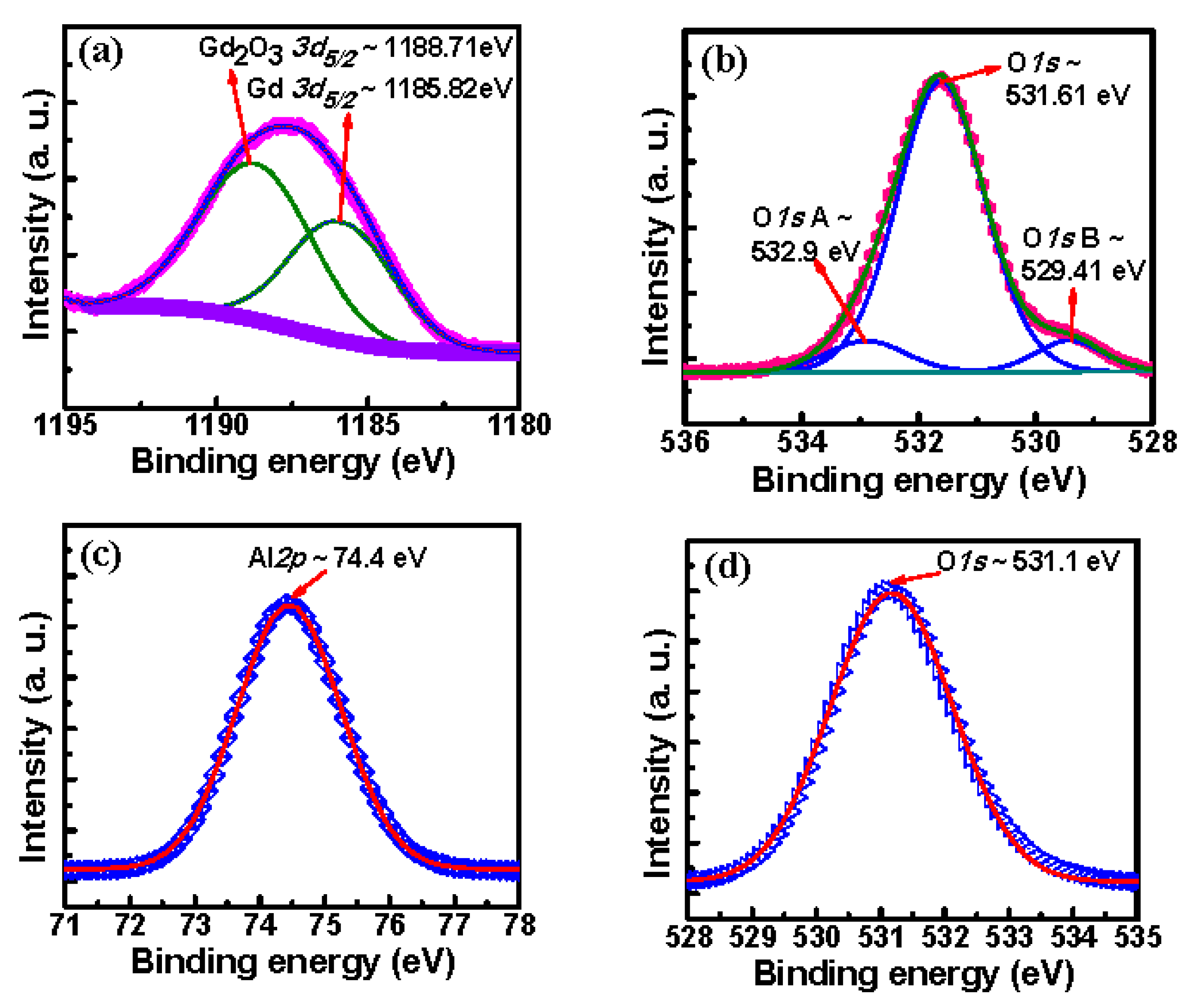
Figure 3.
XRD and AFM characterization. (a) XRD pattern of the GdOx/Si stack which represents the crystalline GdOx film. Three-dimensional (3D) AFM images of (b) SiO2/Si and (c) GdOx/Si stacks with a scan area of 500 × 500 nm2 are shown.
Figure 3.
XRD and AFM characterization. (a) XRD pattern of the GdOx/Si stack which represents the crystalline GdOx film. Three-dimensional (3D) AFM images of (b) SiO2/Si and (c) GdOx/Si stacks with a scan area of 500 × 500 nm2 are shown.
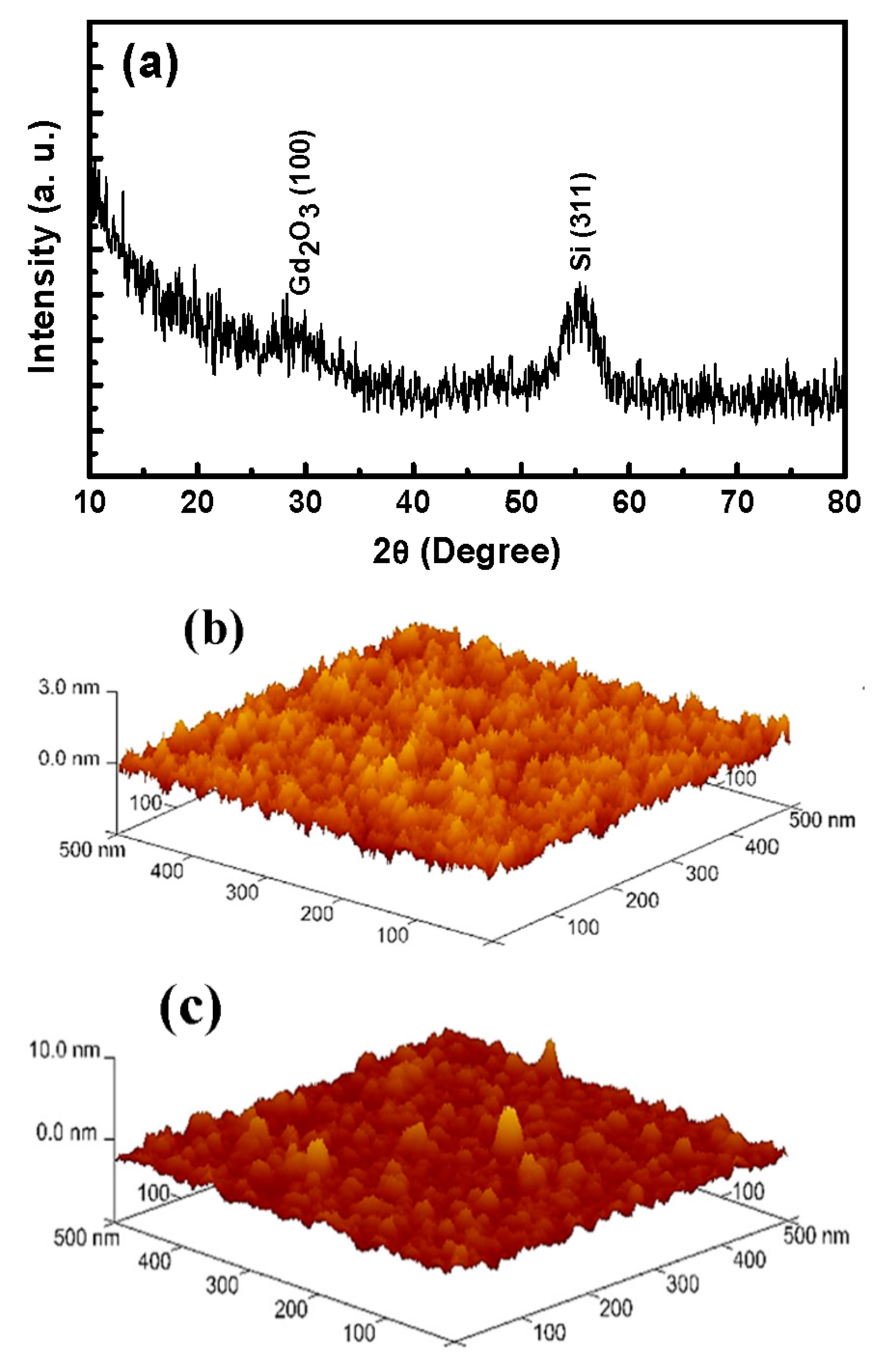
Figure 4.
Current-voltage and current transport characteristics of the S1 and S2 devices. (a) Formation, (b) typical bipolar resistive switching, (c) cumulative probability of leakage current. (d) Space-charge-limited current (SCLC) conduction of the S1 devices, (e) Schottky conduction of the S2 memristor. (f) Schottky conduction at a high resistance state (HRS) is represented by the energy band diagram. Cu migration is also shown.
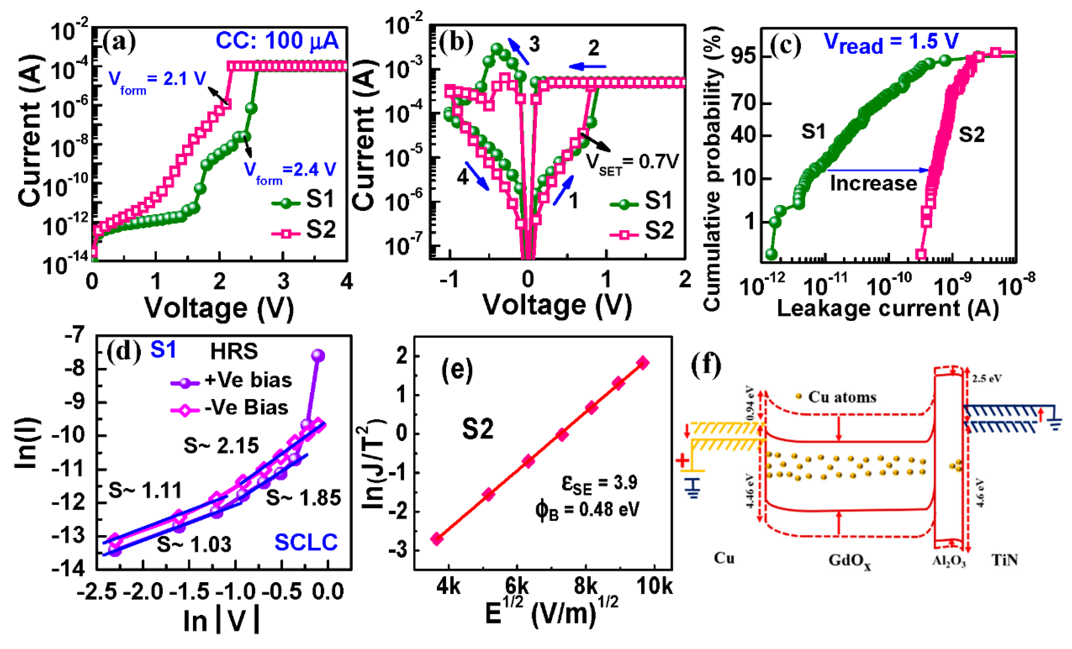
Figure 5.
TEM images, EDS depth profile, and elemental mapping of the S2 devices after SET. TEM image of (a) 0.6 × 0.6 µm sized S2 device and (b) Cu filament. STEM images of (c) with Cu filament and (d) without Cu filament regions are also shown. Elemental depth profiles are measured from Ti to Cu, (e) with Cu filament and (f) without Cu filament regions. Color mapping images of (g) Al, (h) Cu, (i) Gd, (j) O, (k) Ti, and (l) N elements.

Figure 6.
HRTEM images of the S2 devices after SET. (a) Cu TE/GdOx interface without Cu filament and (b) with Cu filament region. Inset of (a) shows the FFT image of Cu, and corresponding d-spacing values.
Figure 6.
HRTEM images of the S2 devices after SET. (a) Cu TE/GdOx interface without Cu filament and (b) with Cu filament region. Inset of (a) shows the FFT image of Cu, and corresponding d-spacing values.
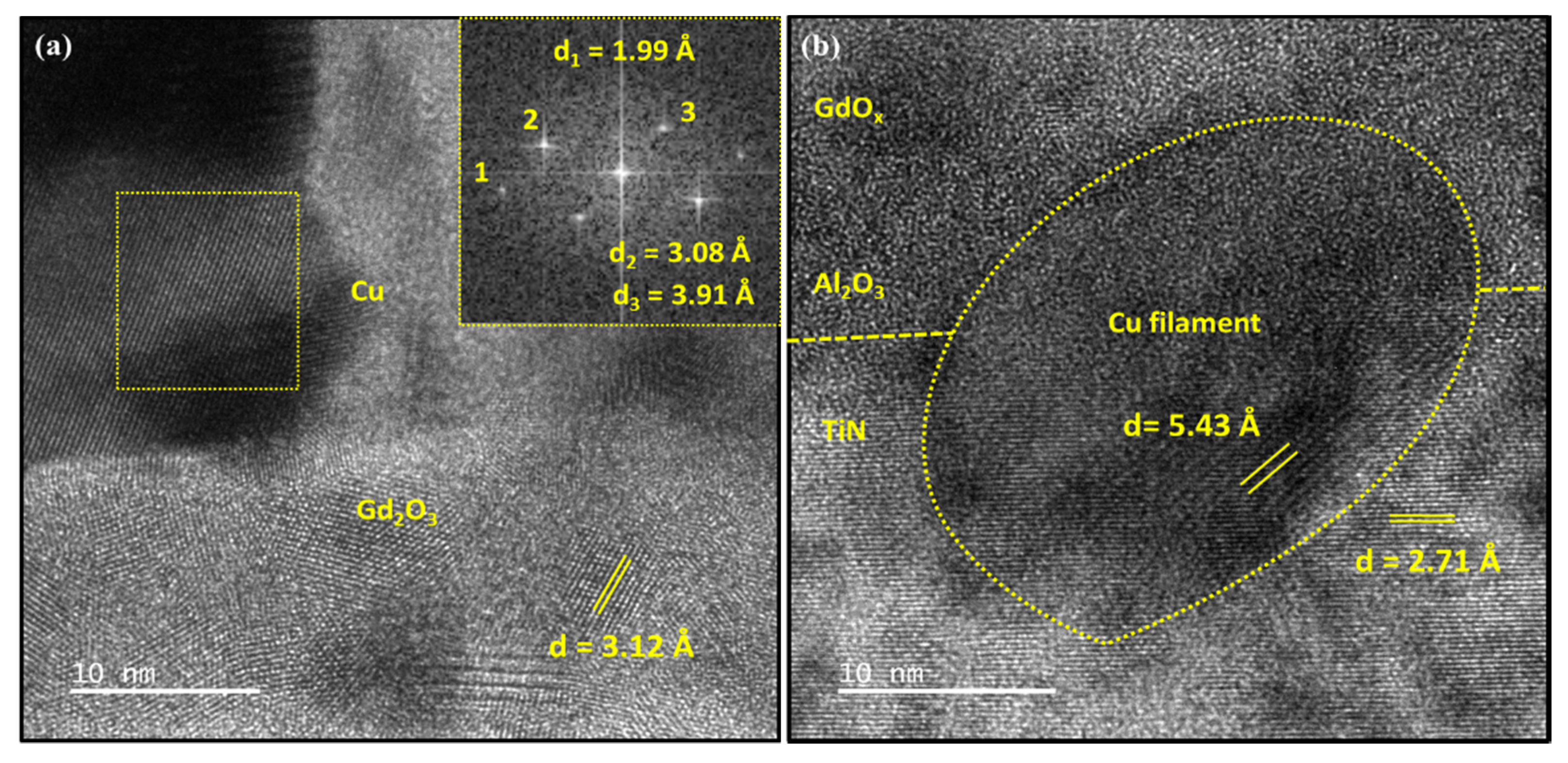
Figure 7.
Bipolar resistive switching performance of the S1 and S2 devices. (a) Comparison of P/E endurance for the S1 and S2 devices with a high speed of 100 ns. The S1 device has shown failure after a few cycles while the S2 device show longer endurance because of Al2O3 interfacial layer. (b) Read endurance of >109 cycles of the S2 devices at a low current of 100 µA. (c) The S2 device also shows longer retention time about 20,000 s with a good stability at low current compliance of 100 µA. (d) The S2 device shows a low current operation of 1.5 µA with a large HRS/LRS ratio of 105 at a read voltage of 0.5 V.
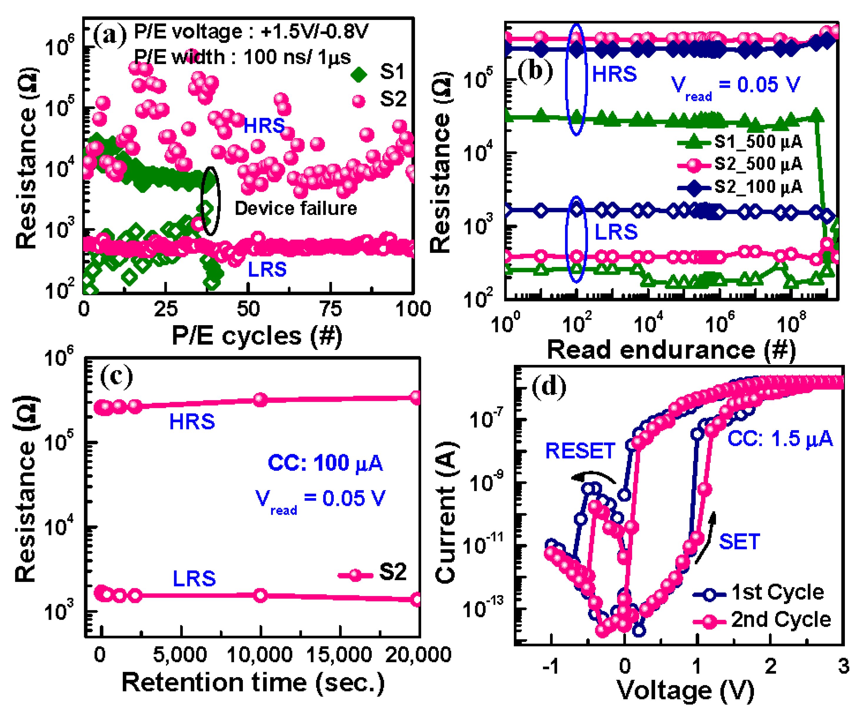
Figure 8.
Complementary resistive switching characteristics of the S1 and S2 memristors with a size of 8 × 8 µm2. Typical CRS characteristics of the (a) S1 and (b) S2 memristors. The S2 device shows a low current operation as compared to the S1 devices because of the Al2O3 interfacial layer. Hopping conduction of the S2 devices under (c) larger hopping distance at the Cu/GdOx interface and (d) smaller hopping distance in the Al2O3 layer. (e) Long read pulse endurance of 1000 cycles at a small pulse width of 1 µs is obtained.
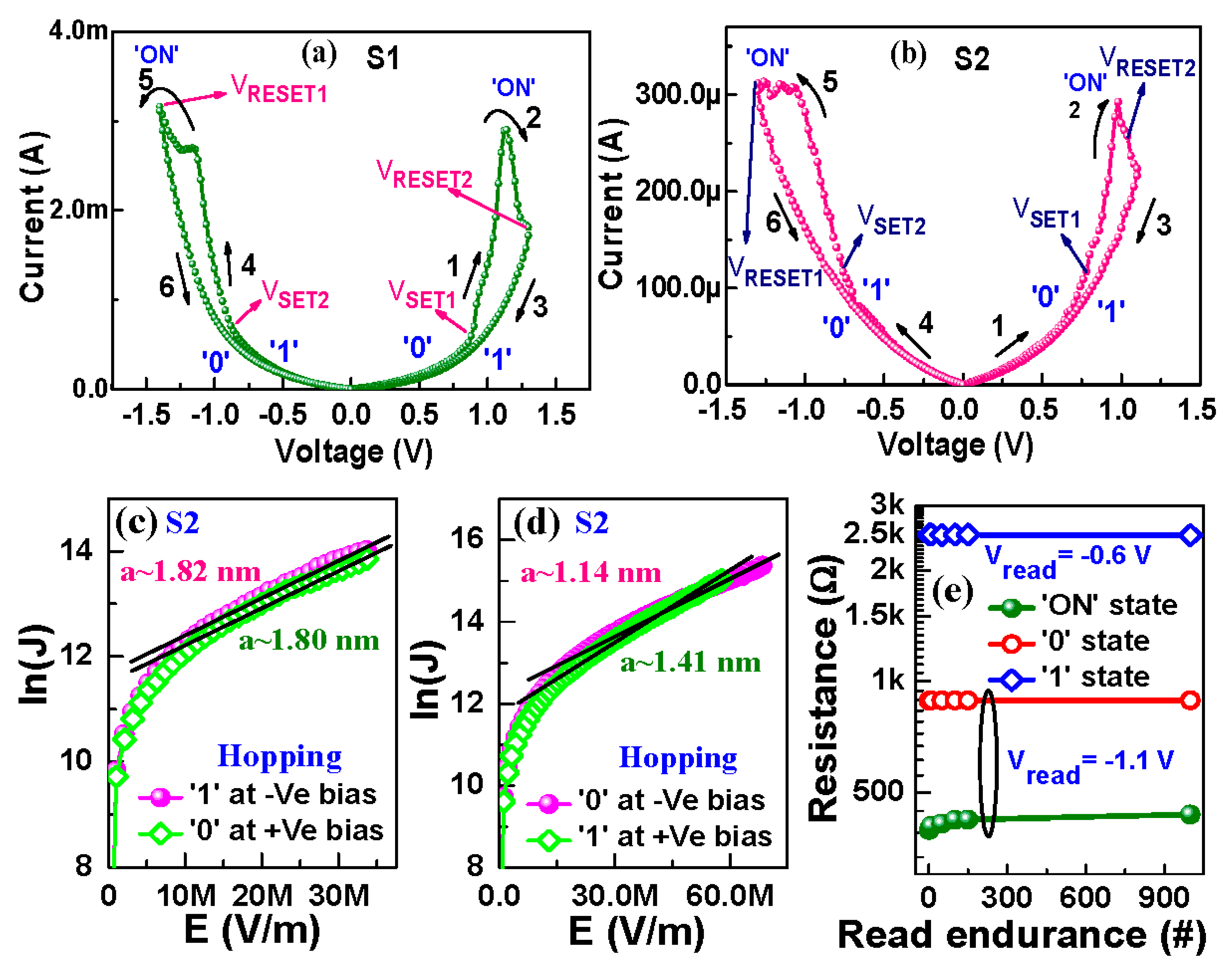
Figure 9.
Schematic demonstration of Cu filament formation/dissolution of CRS characteristics for the Al/Cu/GdOx/Al2O3/TiN structure. (a) Oxygen formation under a negative bias on the TE of a pristine device, (b) “ON” state at >VSET1, (c) “1” state at >VRESET2, (d) “ON” state at <VSET2, and (e) “0” state at <VRESET1. The switching mechanism is due to Cu ions’ migration under controlling an external bias of VRESET1/VRESET2 and the Cu filament is formed/dissolved at the Cu/GdOx interface and in Al2O3 layer.
© 2020 by the authors. Licensee MDPI, Basel, Switzerland. This article is an open access article distributed under the terms and conditions of the Creative Commons Attribution (CC BY) license (http://creativecommons.org/licenses/by/4.0/).
Share and Cite
MDPI and ACS Style
Chiu, C.-F.; Ginnaram, S.; Senapati, A.; Chen, Y.-P.; Maikap, S. Switching Characteristics and Mechanism Using Al2O3 Interfacial Layer in Al/Cu/GdOx/Al2O3/TiN Memristor. Electronics 2020, 9, 1466. https://doi.org/10.3390/electronics9091466
AMA Style
Chiu C-F, Ginnaram S, Senapati A, Chen Y-P, Maikap S. Switching Characteristics and Mechanism Using Al2O3 Interfacial Layer in Al/Cu/GdOx/Al2O3/TiN Memristor. Electronics. 2020; 9(9):1466. https://doi.org/10.3390/electronics9091466
Chicago/Turabian StyleChiu, Chiao-Fan, Sreekanth Ginnaram, Asim Senapati, Yi-Pin Chen, and Siddheswar Maikap. 2020. "Switching Characteristics and Mechanism Using Al2O3 Interfacial Layer in Al/Cu/GdOx/Al2O3/TiN Memristor" Electronics 9, no. 9: 1466. https://doi.org/10.3390/electronics9091466
Note that from the first issue of 2016, this journal uses article numbers instead of page numbers. See further details here.