1. Introduction
NAND flash memory technology has been flourishing since the first flash memory being invented by Dr Fujio Masuoka [
1] in 1984. The development of NAND technology has brought tremendous changes to the memory market and the electronics industry. However, the cost of flash memory still needs to be reduced to gain wider acceptance in mass storage by increasing the storage density. The innovation of etching technology has made NAND flash develop from 2D structure [
2] to 3D structure [
3], and the application of incremental step pulse program (ISPP) scheme [
4,
5] has realized the precise program voltage control, which makes it possible to increase the storage density of NAND flash. The density of storage has been rising from 2D-256Kb single-level cell (SLC) [
6], 2D multi-level cell (MLC) [
7], and 3D MLC [
8], to the current 3D-768Gb triple-level cell (TLC) [
3], 3D quad-level cell (QLC) [
9,
10], and the under-developed penta-level cell (PLC). NAND cells can be designed as
n bits/cell by precisely controlling the levels of the program threshold voltage
, where SLC to PLC stores 1–5 bits/cell corresponding to
–
voltage levels respectively. The high-storage-density NAND flash memories like QLC and PLC start to receive much attention due to the high demands on storage capacity and the low cost. However, the increase in storage density makes the data stored in these NAND flash memories vulnerable to noise interference [
11,
12,
13,
14].
Some error control strategies such as decoding statuses selection [
15], ANN-coupled decoding [
16], retention optimized reading [
13] are of high potential to be applied in the NAND flash memory of high storage density (HSD) to improve its error performance and extend its lifetime, considering that it has more errors and shorter lifetime as the storage density gets higher. The idea is to adopt different strategies for low raw bit error rate (RBER) and high RBER respectively, including using different decoding algorithms for low and high RBER, inputting more accurate soft information to the decoder based on RBER change learned with artificial neural networks (ANN), shifting read reference voltages
s or configuring multi-level
s in read operation when RBER goes high due to
shift. Therefore, having RBER estimated would be a great help to these strategies for memory management and wearing level monitoring. As RBER grows fast in HSD NAND flash, it is very necessary to frequently monitor the RBER in a long term so that the error control methods can be executed at the right time to maintain the performance of the flash. Ref. [
17] proposed a method of using parity violation to estimate RBER, and it needs to multiply a pre-set quantized scalar with the number of parity violations, which is a function of the number of parity violations and determines the accuracy of the estimated BER. However, considering that parity violation can only reflect the odd number of errors in a codeword, it needs a large sample size
N to ensure accurate estimation. For example, it needs to collect
N = 2880 for a 16 KB-page-size flash, which is a very time-consuming collection. The pre-set parameter may not be able to cope with the complex and changing noise condition in HSD flash in time. Hence, it is of hysteresis for HSD NAND flash, where the noise, including Program/Erase (P/E) cycle effects [
12], retention error [
13], and read disturb error [
14], will cause RBER increasing quickly with reading times or P/E cycles and the quickly changed error condition that happens during a read operation is necessary to be measured and reflected in time. Ref. [
18] proposed a fast estimation method by comparing the test data with the data read from the flash memory, but it may not be so suitable for HSD flash memory because frames from different pages have unbalanced error distribution due to data modulation, which can cause inaccuracy in estimation. Meanwhile, the extra redundancy caused by test data reduces the efficiency of reading, especially for the HSD flash which has relatively lower speed but needs the long-term, frequent and in-time RBER monitoring. The read speed of the flash has already been lower than MLC and TLC due to the higher storage density, so to avoid further slowing down, the RBER estimation method should not slow down or even would be better to speed up the reading process.
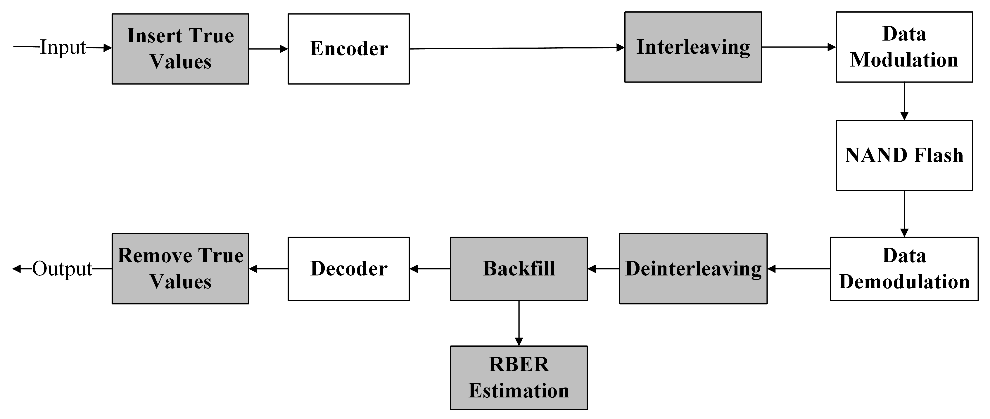
In this paper, we proposed an improved and easy-to-implement fast RBER estimation method for HSD NAND flash utilizing true-value data comparison, which can also strengthen error performance of error control code (ECC), thereby increasing reading efficiency of the flash. The method includes an interleaving module to balance the errors from different pages, an RBER estimation module, and enhancement strategies for hard-decision and soft-decision decoding to improve error performance.
The rest of the paper is organized as follows.
Section 2 explains how the data modulation affects the error distribution on pages and how the interleaving module alleviates the unbalance.
Section 3 describes the procedure and parameter setting of the RBER estimation.
Section 4 depicts the strategies of improving error performance of ECC by using extrinsic information from the redundant true-value data.
Section 5 presents a hardware implementation of the proposed method.
Section 6 draws a conclusion.
2. Data Modulation in NAND Flash
Data modulation refers to how to map the bit codes to a voltage level programmed into a NAND flash cell. The distribution of bit errors in the NAND flash highly depends on the pattern of data modulation. The currently widely used data mapping method is 1/2 division gray coding, or 1/2 gray coding for short. The term “1/2 division” means that the first line of the mapping table is divided by “1” and “0” in half, and each line half-divides the previous line by “1” and “0” again, as shown in
Figure 1a. Another pattern is balanced gray coding, which is mentioned in [
19] as an alternative for QLC data modulation. The term “balanced” means that each line of the mapping table has almost the same times of toggling between “1” and “0”. Since the errors in the flash is mainly due to the
in the cell being shifted to the neighbouring levels by the noise interference, using gray coding can minimize the number of bit errors caused by the shift.
Data are programmed or erased in the NAND flash cells through the Fowler–Nordheim (FN) tunnelling effect [
20]. The level of the program voltage can be controlled by how much charge the cell stores since the program voltage is proportional to the tunnelling charge density in the cell. When the 1/2 gray coding data modulation is used, the data are stored via ISPP, which increases the threshold voltage
step by step to charge a cell to a certain program voltage level. The tunnelling electrons of the cell are gradually stored and accumulated to a certain level as required. When the balanced gray coding method is used, the data are stored in a cache first, and the cells are then charged to the voltage levels by incremental steps or in one pass.
Data are read from cells by comparing
with
s on each page to demodulate them to corresponding codes, as shown in
Figure 1a,b. However, the widths of discriminant intervals are different on pages and wider interval has a higher tolerance to errors caused by the shift of
. Therefore, the frames from the upper page have higher frame error rates (FER) than the lower page. The experimental data of MLC in [
21] shows that the error rate on the upper page has already been slightly higher than the lower page. Although the difference is not much problematic in MLC because of its low storage density, it will be in QLC and PLC as the storage density goes higher and FER of the most upper page can become huge, as shown in
Figure 2 and
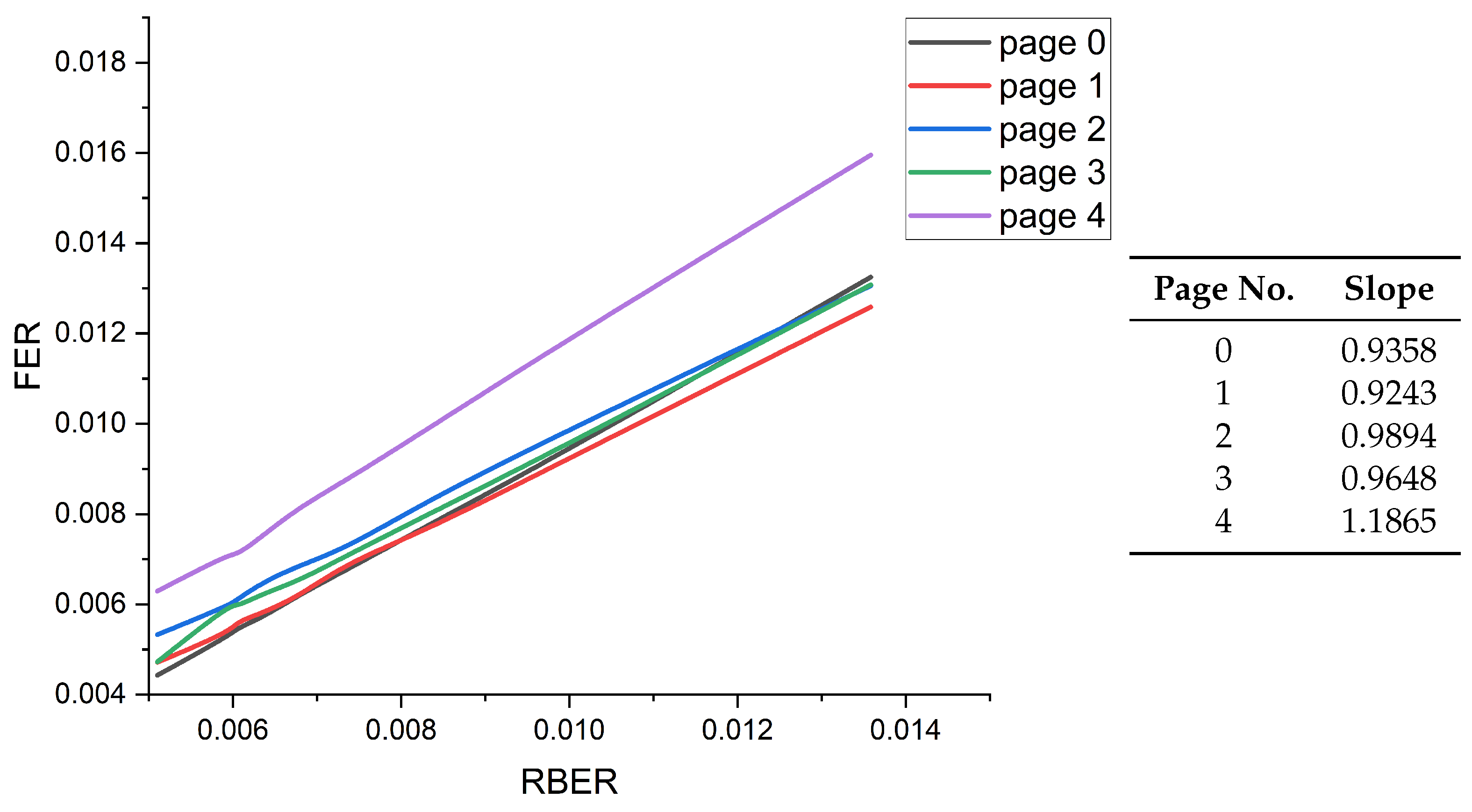
Figure 3. The unbalanced page error rates (PER) will cause inaccuracy in RBER estimation. The balanced gray coding modulation has less unbalanced PER, but there is still at least one page having higher PER than the others. We use PLC to illustrate the situation because it is the flash of the highest storage density currently known, so the situation is more obvious on it. As shown in
Figure 2, the PERs are hugely unbalanced when 1/2 gray coding modulation is used, and frames from page 4 have FERs about 2.5 times as high as the RBER of the NAND flash. Meanwhile, the errors grow much faster on upper pages that the slope of page 4 is 9.7 times of page 0. Consequently, a very large FER will appear on page 4, causing inaccurate estimation as the sample frames are from different pages. When the balanced modulation is used, in
Figure 3, the PERs are still not completely balanced that the frames from page 4 still have FERs about 1.5 times of the RBER, which will also affect the accuracy.
The accuracy of RBER estimation will be affected by whether every frame sampled for the RBER estimator having similar FER. Since both types of modulation are possibly used in HSD flash, it is important that the RBER estimation method can be compatible with them both to balance the errors.
To meet this requirement, an interleaving module is applied to alleviate the effect of the data modulations and making FERs of each frame as equally as possible, in order to achieve more accurate estimation. Interleaving is to swap the places of the message bits in the frames before modulating them to voltage levels. Correspondingly, a deinterleaving module is applied to restore the swapped message bits after the frames are retained. In our implementation, we built a uniformly randomly generated lookup table to allocate each bit to a specific position and the same lookup table will be used for all frames. For example, message bit 1 is allocated to position 5, bit 2 is allocated to position 11, and so on. The interleaving aims to spread the message bits evenly across the memory cells. The deinterleaving restores the original order of the message bits by using the lookup table reversely. For instance, the bit in position 5 is back to message bit 1, and the bit in position 11 is back to bit 2, and so on. The interleaving scheme is not unique, one can apply other interleaving schemes for his own design purposes. The effect of interleaving depends on the length of the interleaved message bits and can be measured with the variance of FERs. As shown in
Figure 4, the effect is better when the interleaved message bits become longer, but the variance drops slowly when the length exceeds 500 and almost no longer drops when the length exceeds 1200. Considering that the longer interleaving requires larger read-only memory and takes more clock cycles, which will increase the hardware complexity and extend processing time, it is recommended that interleaving a message in every 1024 bits is sufficient. As shown in
Figure 5 and
Figure 6, for both types of data modulation, interleaving makes the disturbed bits evenly distributed to each frame and turns the increasing rates of FERs from each page to almost the same.
3. RBER Estimation
The RBER is estimated by comparing the true-value sequence inserted into specific positions of each frame with the one read from the flash to get an estimated FER. To ensure the accuracy of the estimated RBER, averaging the estimated FERs of multiple sample frames is required. The accuracy depends on two factors, the length of the true-value sequence L and the number of sample frames N. With the interleaving module to balance the errors of frames from different pages, there will be no huge difference in FERs obtained from the frames. Otherwise, it may result in inaccurate estimation in HSD NAND flash.
We estimated RBER with the mean of
N = 16 sample frames because the division by 16 in estimation can be implemented with a right shifter. Moreover, it is a short time to wait and collect 16 frames in the HSD NAND flash, especially when the parallel structure of encoding and decoding is used, so the RBER of the flash can be reflected in time. The larger
N can certainly lead to more accurate estimation, but it will take longer. The length
L of the true-value sequence should also be selected carefully because a too-long sequence will cause too much rate penalty, whereas a too-short one will cause inaccurate estimation.
Figure 7 shows how the lengths of the true-value sequence affect the mean square error (MSE) between
, the estimated BER, and the actual RBER when tested with a (10,080, 8400) QC-LDPC from [
22]. The MSE is about
at the length of 200/8400, about 5 times larger than
at 300/8400, and then stays at the same order of magnitude down to
at 400/8400. Namely, the MSE is decreasing with the increase of the length, but the trend is gradually slowing down when the length exceeds 300/8400. To balance the rate penalty and the accuracy of estimation, the length is suggested to be less than 3.5% of the total length of the frame. We set
L = 256 in our test for the convenience of hardware implementation.
Figure 8 illustrate two cases of estimation at RBER = 0.01 and 0.1. In the HSD flash using 1/2 gray coding modulation, the estimation is very inaccurate when directly comparing data without interleaving. In this case, only 55.49% and 36.99% of the estimated values fall in [0.009, 0.011] and [0.09, 0.11], respectively, the
% range of the actual RBER. The interleaving module greatly improves the accuracy of the estimation for such flashes, making 85.37% and 99.55% of the estimated values fall within [0.009, 0.011] and [0.09, 0.11], respectively, and significantly narrowing the distribution interval. For the flash using balanced gray coding modulation, where about 83.4% and 97.89% of the estimated values are located within [0.009, 0.011] and [0.09, 0.11], respectively, interleaving only slightly increases the accuracy and narrows the distribution interval. Nevertheless, in general, interleaving can improve the accuracy of RBER estimation in HSD NAND flash using either modulation.
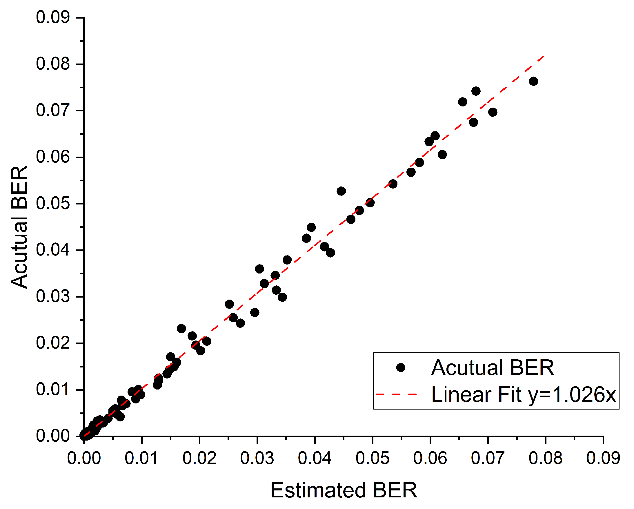
Figure 9 shows that with the interleaving, the method can make
very close to the actual RBER, and they are highly linearly correlated though there exist some small fluctuations. Therefore, it is credible to estimate RBER in NAND flash with the true-value insertion method equipped with interleaving, and the good linearity can make the
sensitive to RBER change. Hence, it is suitable to measure and reflect RBER in HSD NAND flash in time.
can help select decoding statuses. Usually, the soft-decision decoding is selected after the default reading level with hard-decision decoding and retry level with hard-decision decoding are failed, which wastes time on trial and error. Based on the current BER estimated, the decoding status can be directly selected so that the controller does not have to try through all decoding statuses, which thereby increase the reading speed for NAND flash. To realize this, a threshold RBER can be set to trigger switching between hard-decision and soft-decision decoding statuses that hard-decision decoding is applied when <, and the soft-decision decoding is used otherwise. The method can also be used for cell wearing monitoring. The RBER will be rising when NAND flash cells are gradually wearing out as the number of P/E cycles increasing, so the long-term recorded s can reflect the cell wearing condition in NAND flash. A block is possibly being worn out when its reaches a certain threshold, and the controller should be informed to execute error management strategies or migrant the data to other blocks.
4. Enhancement Strategy for Decoding
Since the HSD NAND flash has high storage space but relatively lower read speed, we care more about reading performance than the extra storage space taken up. We hereby proposed the enhancement strategies to accelerate decoding convergence with extrinsic information from the redundancy, making up the rate penalty caused by it.
To detect and correct errors in HSD NAND flash, the low-density parity-check codes (LDPC) [
23,
24] are usually used, which are suitable for scenarios that the code rates are higher than 2/3 [
25]. Typically, the code rate in NAND flash is above 0.8 and even reaches 0.95, and the block length is also very large, up to 8 Kbit or even 20 Kbit [
26,
27,
28]. Moreover, the encoding and decoding of LDPC can be easily implemented in parallel to increase throughput [
22,
29,
30,
31]. Among types of LDPC codes, quasi-cyclic LDPC (QC-LDPC) code [
32] is a structured LDPC code recommended because it satisfies the row/column constraint to make sure no loop iteration in decoding which otherwise can result in decoding failure [
33,
34,
35]. The decoding of QC-LDPC can have no error floor down to
[
29].
There are two kinds of LDPC decoding algorithms, hard-decision decoding and soft-decision decoding. The hard-decision directly converts received symbols into demodulated bits “0” or “1”, whereas the soft decision is based on the probability of received symbols, expressed using logarithmic likelihood rate (LLR), to decide the most likely value for the corresponding bit. LLR is presented as
where
is the LLR value,
is the transmitted bit, and
is the received bit. The posterior probability
is determined by BER of the received codeword. The hard-decision decoding algorithms include majority logic decoding and bit flip decoding [
23], which are characterized by low complexity, fast speed, but weak error correction capability. The most widely used soft-decision decoding algorithms are sum–product algorithm (SPA) and minimum sum algorithm (MSA), a simplification of SPA [
24,
30]. The computational complexity of soft-decision algorithms is much higher than the hard-decision ones, but their error-correction capability is stronger.
Figure 10 represents our enhancement strategies for bit-flip decoding and SPA decoding. The content and position of the true-value sequence are known. For bit flip decoding, as in
Figure 10a, denote the position of true-value sequence as
, the number of parity violation for each bit of the read codeword as
, the positions of the maximum in
f as
, and the position of bit flipping as
. Before decoding starts, fill back the true values to the read codeword. Then, calculate the number of parity violation for each bit. Find the positions where the maximum number of parity violations are, and remove the positions of the true values if there is any to get the position of the bits to be flipped
. While
is null, give
the positions of the second maximum in
f. Repeat the above procedures until there is no parity violation or the program reaches its max iterations. As shown in
Figure 11, the enhancement strategy gives the bit flip decoding better error performance, so more errors can be corrected by hard decision in the same number of iterations. Therefore,
can be slightly increased in switching decoding statuses accordingly, and more decoding can use the hard-decision algorithm. The flash reading speed is thus increased at lower RBER. For SPA decoding, as
Figure 10b, denote
as variable node
j,
as check node
i,
as the LLR of variable node
j,
as the value passed by variable node
j to check node
i, and
as the value passed by check node
i to variable node
j. Before decoding starts, the LLRs at the positions of the true values are set to very large values, usually at least 10 times larger than the others, because we have a strong belief that the true values backfilled are correct. The LLRs will be propagated as the initial values of
and
.
is updated with
of each
connected to
, and then
is updated with
of each
connected to
. The
is then updated with
, where
M is the total number of check nodes. Then
is discriminated based on
and parity check is done for
. The above procedures are repeated until there is no parity violation, or the program reaches its max iterations. As shown in
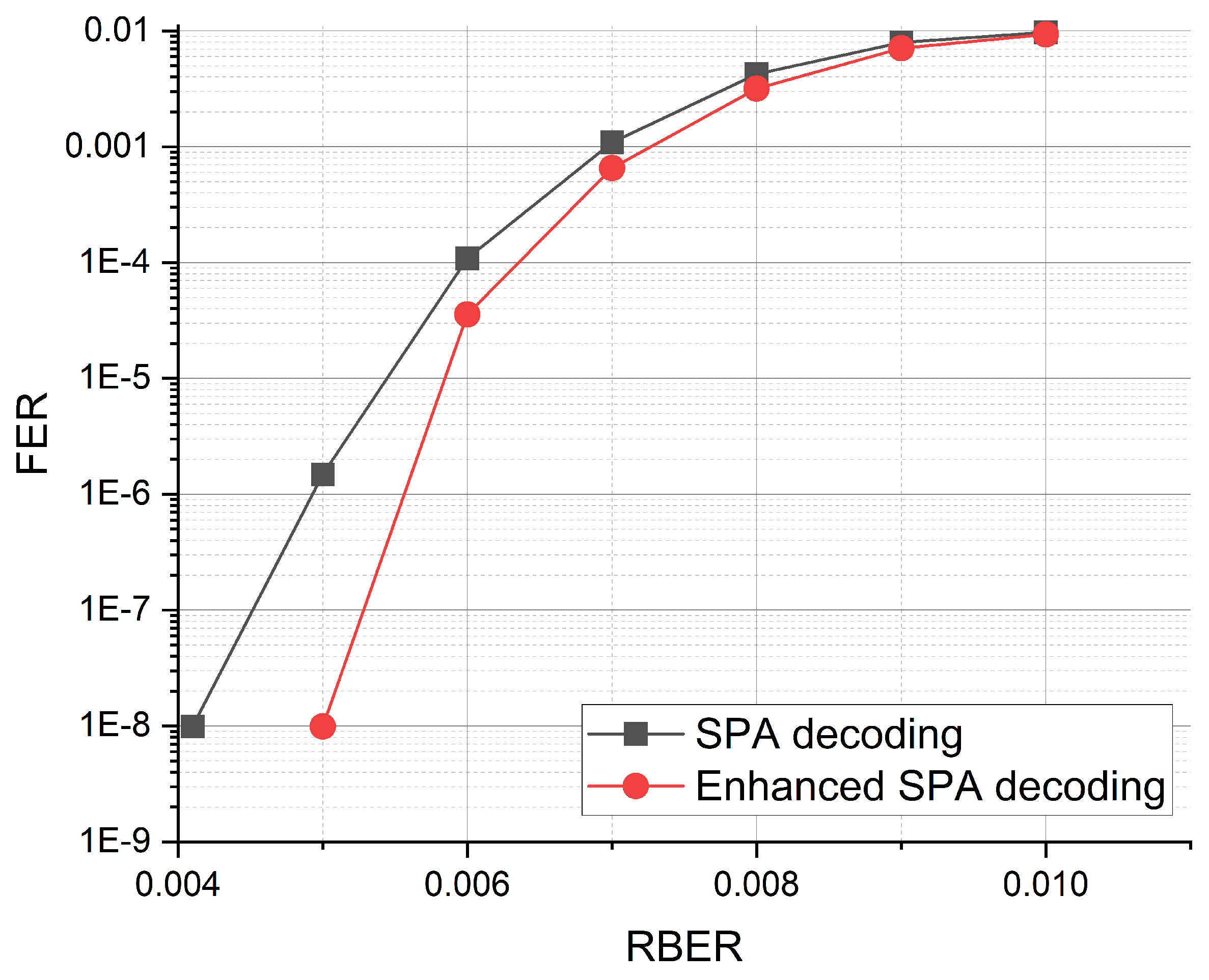
Figure 12, with the enhancement strategy, the SPA decoding achieves better error performance and converges faster at higher RBER, which means that some iterations can be saved in decoding. The iteration of soft-decision decoding is time-consuming, compared with hard-decision decoding, so saving iterations can certainly improve the read speed, especially at higher RBER.
Taking QC-LDPC (10,080, 8400) [
22] as an instance for latency analysis, whose parity check matrix has 288 non-zero circulants, supposing that the decoder is capable to process one circulant per clock, the decoder requires 288 clock cycles to finish an iteration. As shown in
Figure 13, when RBER = 0.008, the average number of iterations at
is 10 iterations with the proposed enhancement strategy whereas the iteration time is 18 without it. Supposing that 64 bits are read from the memory per clock cycle, the interleaving and de-interleaving each takes
clock cycles, and true-value sequence inserting, backfilling and removing each takes extra
clock cycles. Hence,
clock cycles can be saved in every decoding, which indicates that the read is sped up by 38.12%. Hence, the enhancement strategy can strengthen the error performance of SPA and thus speed up reading operation when RBER becomes high to the upper bound of ECC. From the perspective of transmission efficiency, decoding 28 frames with the redundancy transmits almost as much amount of data as decoding 27 frames without the redundancy. The former takes
= 89,824 clock cycles whereas the latter takes
= 139,968 clock cycles, so the former saves 50,144 clock cycles when transmitting almost the same amount of data, which is equivalent to a 35.8% increase in efficiency.
The difference of the iterations gets larger when RBER gets higher, especially when RBER reaches the upper bound of the LDPC code, which is 0.01 in this case. Since the maximum iterations are set much less than 70 in practice, such a frame may be judged as a decoding failure and will be switched to re-read status, which will take much more clock cycles than the soft-decision decoding. Namely, the ECC can correct more error patterns with the enhancement strategy under the same decoding status. The HSD NAND flash tends to produce high RBER, so the proposed enhancement strategy can save many clock cycles for it and thus improve read performance. Since the flash cares more about read performance than storage space, the proposed enhancement strategy will be helpful at both lower and higher RBER, especially when RBER reaches a high value near the upper bound of the ECC. Therefore, the redundancy brought by the true-value sequence is worth the increase in the converging speed of decoding.
6. Conclusions
This paper proposed a fast, read-performance-improving, and low-cost RBER estimation method suitable for HSD NAND flash, including interleaving, RBER estimating and enhancement strategies for decoding. Interleaving alleviates the effect of unbalanced error distribution on pages caused by data modulation and thus improves accuracy for RBER estimation. RBER estimation is achieved with true-value data comparison, which can make estimation fast. The estimated BER is close to the actual one and they are highly linearly correlated, so the estimated BER can be sensitive to RBER change and reflect it in time. However, the redundancy brought by the true-value data reduces reading efficiency of the flash, so to solve the problem, two enhancement strategies are proposed to improve error performance of ECC in both hard-decision and soft-decision decoding. For hard-decision decoding, the improvement can raise the in decoding status selection so that some frames with relatively higher FER, which should have been decoded with soft-decision, can be decoded by the hard-decision decoding. Considering that hard-decision decoding has much lower computational complexity than soft-decision decoding, the enhancement will improve read performance at low RBER. For soft-decision decoding, the enhancement strategy speeds up the decoding convergence so that errors can be corrected with fewer iterations. Moreover, with the enhancement strategy, the frames with high FER close to the upper bound of ECC can be corrected within the maximum iteration times without falling in re-read status, which will take much longer than soft-decision decoding. Hence, the read performance at high RBER is also increased. The hardware complexity of the proposed RBER estimation method is very low. Therefore, the method has a high potential for long-term and frequent monitoring on RBER in HSD NAND flash.
Incidentally, more applications of the proposed method can be developed. The future work will focus on designing a reading mechanism with a neural network aided by the RBER estimation to soft sense the shift for the SPA decoder to achieve better error correction performance.


