Switching Characteristics and Mechanism Using Al2O3 Interfacial Layer in Al/Cu/GdOx/Al2O3/TiN Memristor

 and
and 
Abstract
:1. Introduction
2. Materials and Methods
Memristor Fabrication Process
3. Results and Discussion
3.1. Material Characteristics
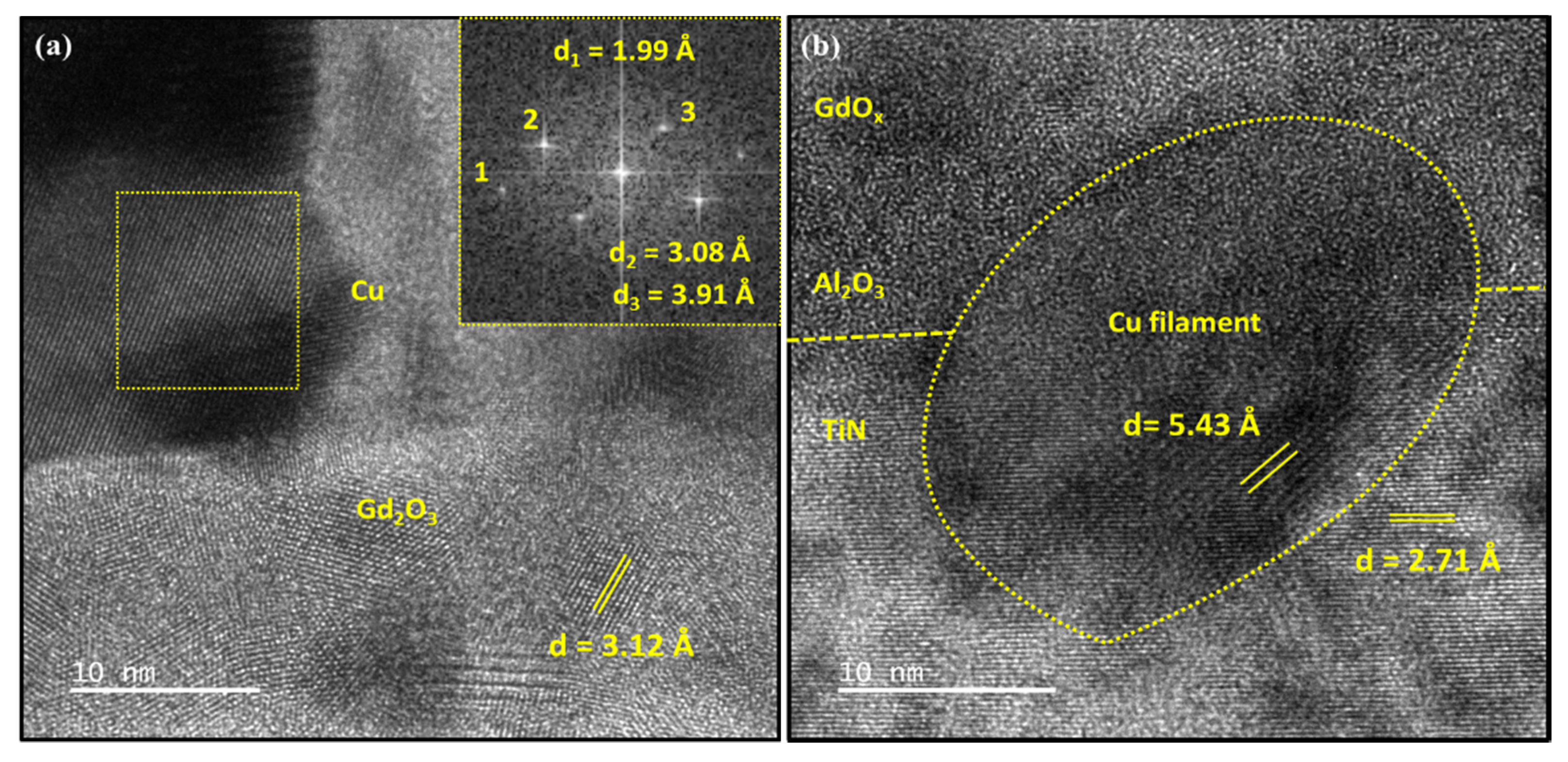
3.1.1. TEM Image of Pristine Memristor
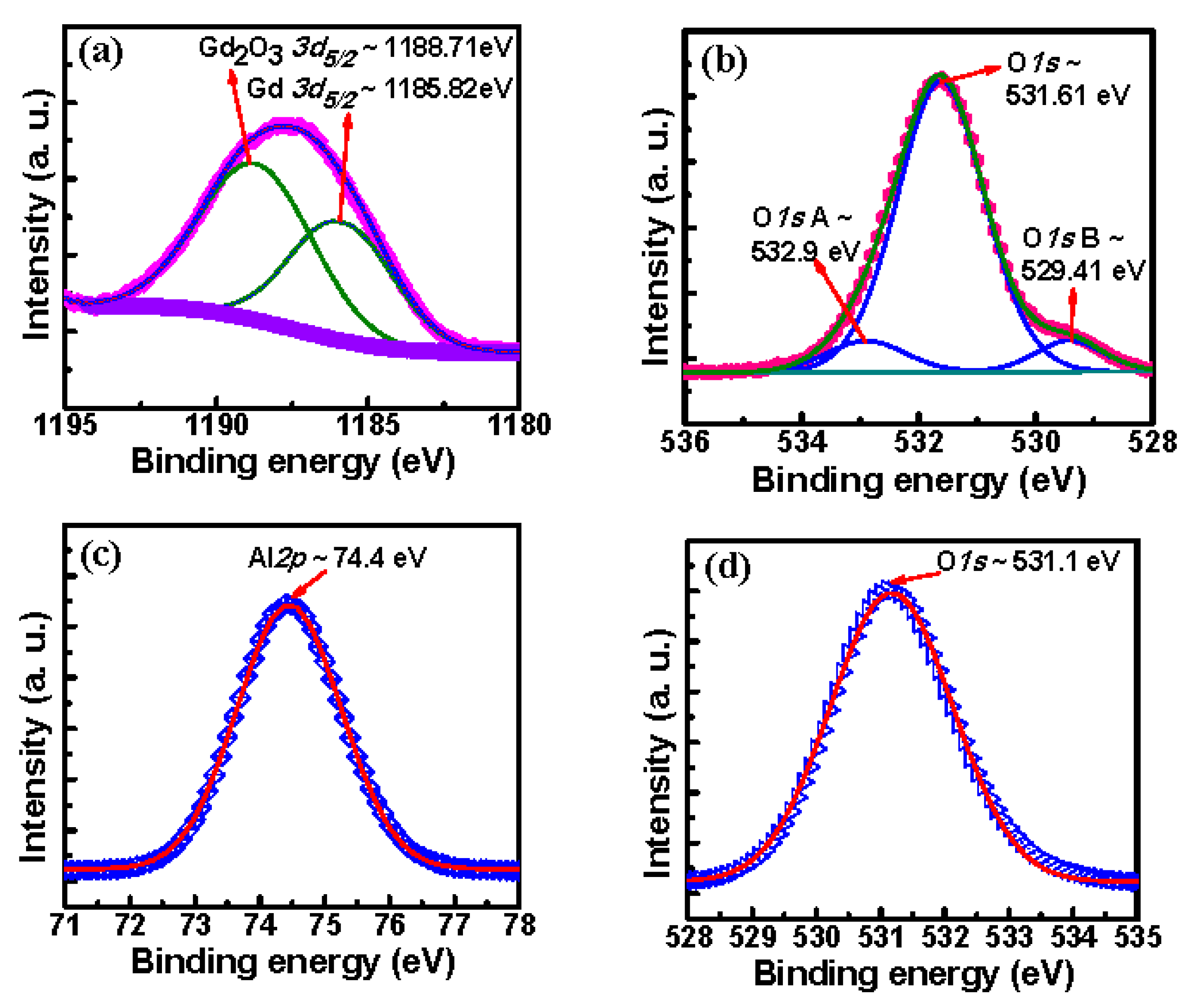
3.1.2. XPS Analysis
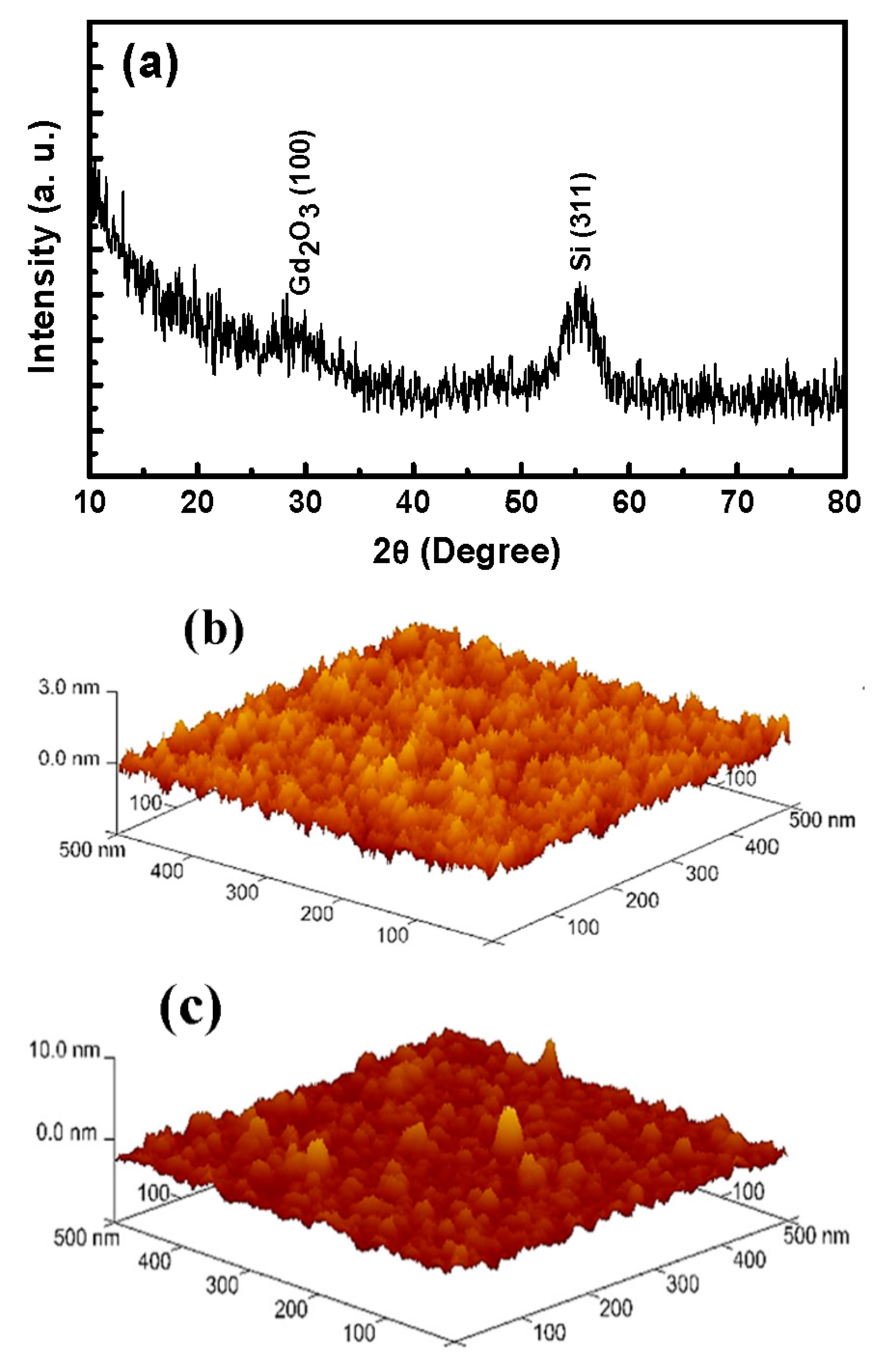
3.1.3. XRD Pattern and AFM Image
3.2. Bipolar Resistive Switching Characteristics
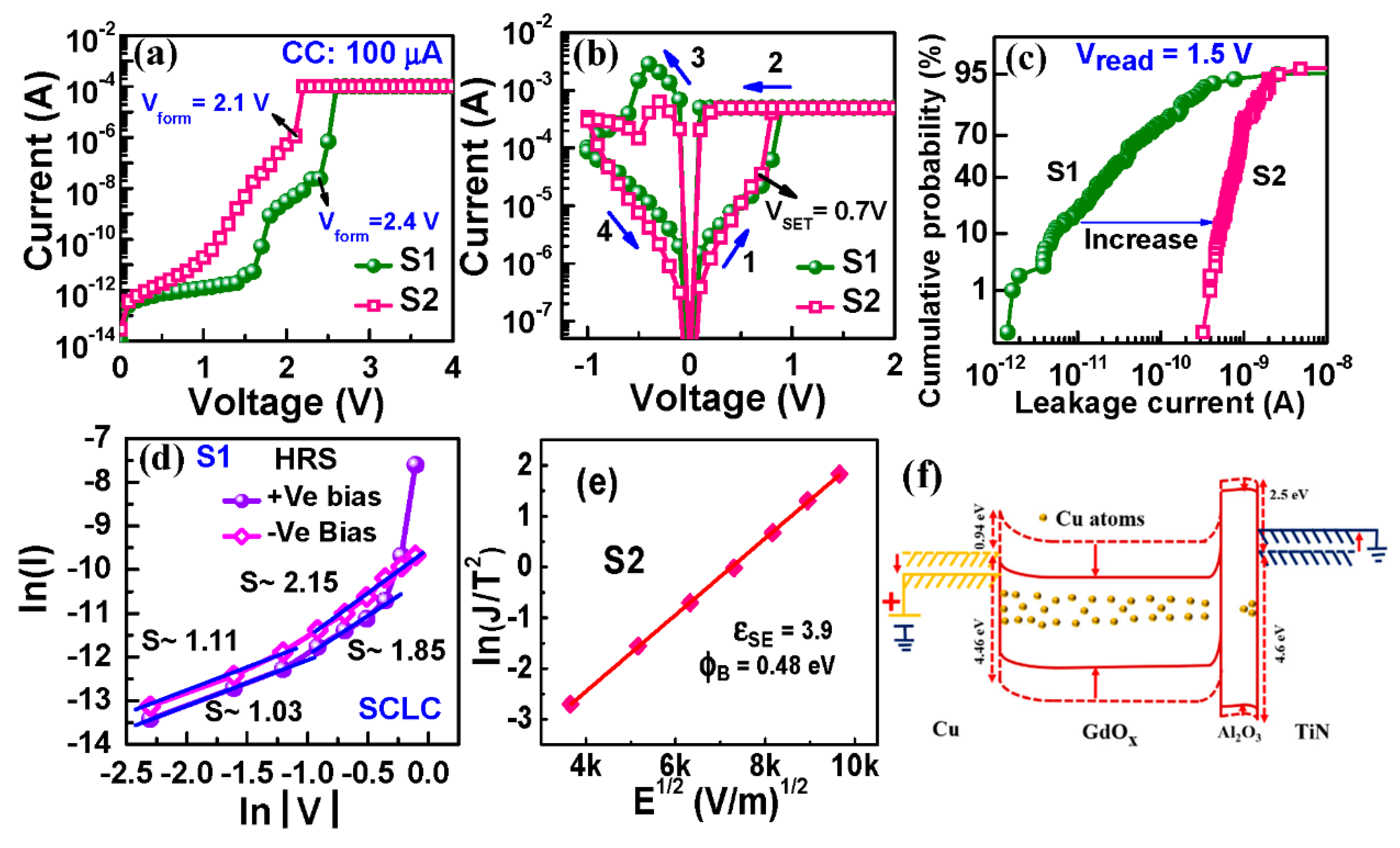
3.2.1. Current-Voltage Switching and Transport Mechanism
3.2.2. Evidence of Cu Migration
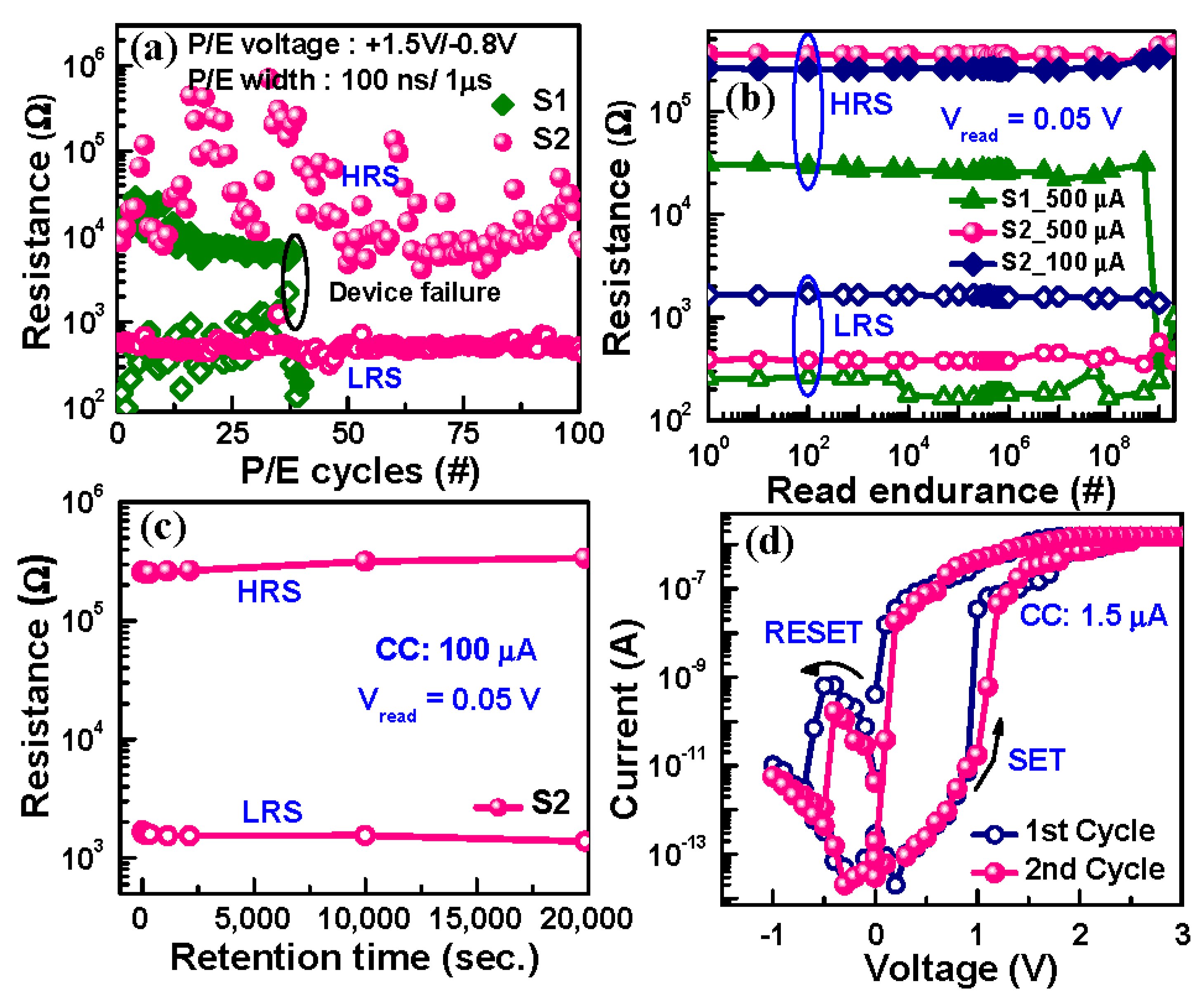
3.2.3. Device Performance and Low Current Operation
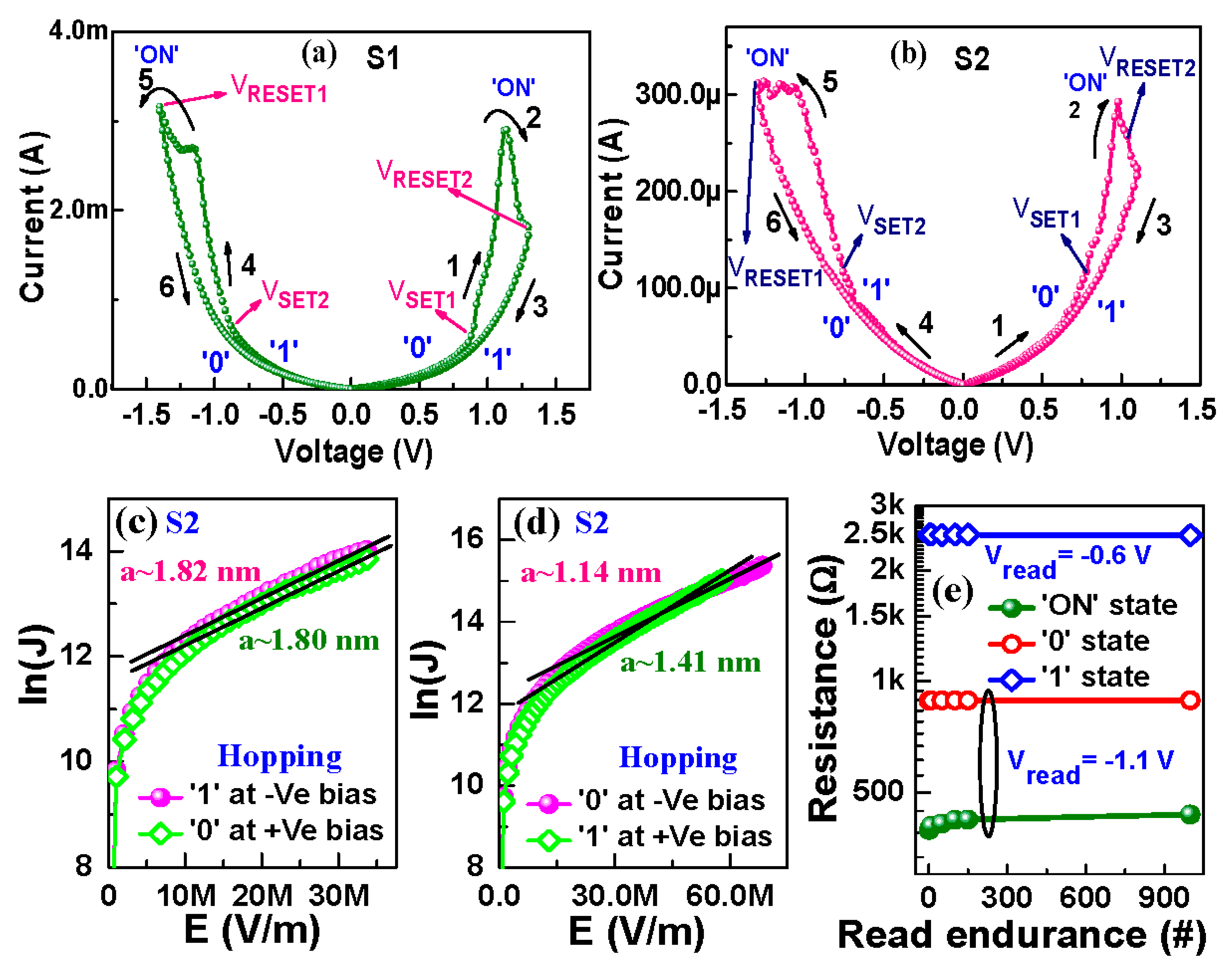
3.3. CRS Phenomena
3.3.1. I–V and Transport Characteristics
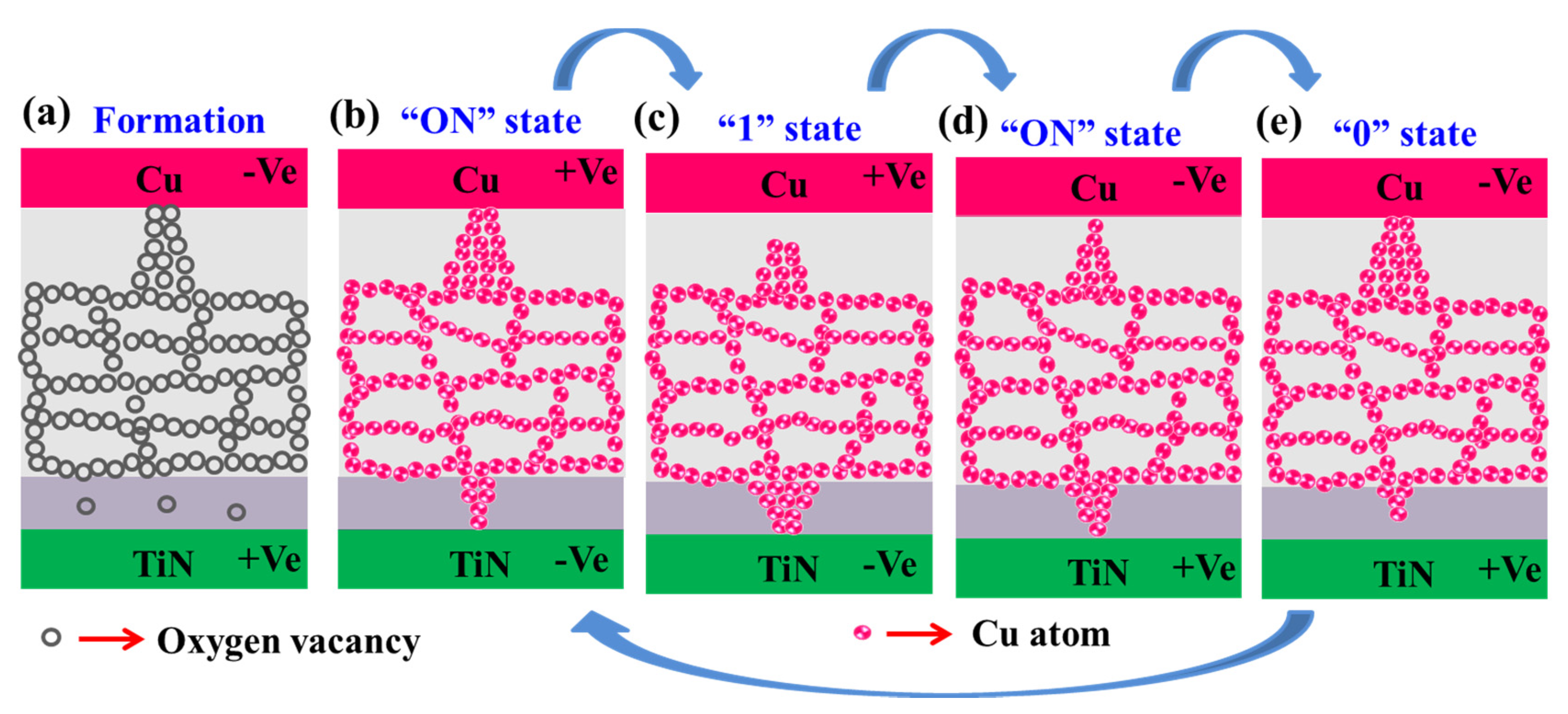
3.3.2. Memristor Mechanism
4. Conclusions
Supplementary Materials
Author Contributions
Funding
Acknowledgments
Conflicts of Interest
References
- Banerjee, W. Challenges and applications of emerging nonvolatile memory devices. Electronics 2020, 9, 1029. [Google Scholar] [CrossRef]
- Slesazeck, S.; Mikolajick, T. Nanoscale resistive switching memory devices: A review. Nanotechnology 2019, 30, 352003. [Google Scholar] [CrossRef]
- Waser, R.; Aono, M. Nanoionics-based resistive switching memories. Nat. Mater. 2007, 6, 833–840. [Google Scholar] [CrossRef] [PubMed]
- Pan, F.; Gao, S.; Chen, C.; Song, C.; Zeng, F. Recent progress in resistive random access memories: Materials, switching mechanisms, and performance. Mater. Sci. Eng. R Rep. 2014, 83, 1–59. [Google Scholar] [CrossRef]
- Jana, D.; Roy, S.; Panja, R.; Dutta, M.; Rahaman, S.Z.; Mahapatra, R.; Maikap, S. Conductive-bridging random access memory: Challenges and opportunity for 3D architecture. Nanoscale Res. Lett. 2015, 10, 188. [Google Scholar] [CrossRef] [PubMed] [Green Version]
- Maikap, S.; Banerjee, W. In quest of nonfilamentary switching: A synergistic approach of dual nanostructure engineering to improve the variability and reliability of resistive random-access-memory devices. Adv. Electron. Mater. 2020, 6, 2000209. [Google Scholar] [CrossRef]
- Dutta, M.; Maikap, S.; Qiu, J.T. Controlling conductive filament and tributyrin sensing using an optimized porous iridium interfacial layer in Cu/Ir/TiNxOy/TiN. Adv. Electron. Mater. 2019, 5, 1800288. [Google Scholar]
- Ginnaram, S.; Qiu, J.T.; Maikap, S. Role of the Hf/Si interfacial layer on the high performance of MoS2-basedconductive bridge RAM for artificial synapse application. IEEE Electron Device Lett. 2020, 41, 709–712. [Google Scholar] [CrossRef]
- Senapati, A.; Roy, S.; Lin, Y.-F.; Dutta, M.; Maikap, S. Oxide-electrolyte thickness dependence diode-like threshold switching and high on/off ratio characteristics by using Al2O3 based CBRAM. Electronics 2020, 9, 1106. [Google Scholar] [CrossRef]
- Belmonte, A.; Radhakrishnan, J.; Goux, L.; Donadio, G.L.; Kumbhare, P.; Redolfi, A.; Delhougne, R.; Nyns, L.; Devulder, W.; Witters, T.; et al. Co active electrode enhance CBRAM and scaling potential. In Proceedings of the IEEE International Electron Devices Meeting 2019, San Francisco, CA, USA, 7–11 December 2019. [Google Scholar]
- Kim, S.M.; Kim, H.J.; Jung, H.J.; Kim, S.H.; Park, J.Y.; Seok, T.J.; Park, T.J.; Lee, S.W. Highly uniform resistive switching performances using two-dimensional electron gas at a thin-film heterostructure for conductive bridge random access memory. ACS Appl. Mater. Interfaces 2019, 11, 30028–30036. [Google Scholar] [CrossRef]
- Roy, S.; Maikap, S.; Sreekanth, G.; Dutta, M.; Jana, D.; Chen, Y.Y.; Yang, J.R. Improved resistive switching phenomena and mechanism using Cu-Al alloy in a new Cu:AlOx/TaOx/TiN structure. J. Alloys Compd. 2015, 637, 517–523. [Google Scholar] [CrossRef]
- Hubbard, A.W.; Kerelsky, A.; Jasmin, G.; White, E.R.; Lodico, J.; Mecklenburg, M.; Regan, B.C. Nanofilament formation and regeneration during Cu/Al2O3 resistive memory switching. Nano Lett. 2015, 15, 3983–3987. [Google Scholar] [CrossRef] [PubMed] [Green Version]
- Banno, N.; Sakamoto, T.; Iguchi, N.; Sunamura, H.; Terabe, K.; Hasegawa, T.; Aono, M. Diffusivity of Cu ions in solid electrolyte and its effect on the performance of nanometer-scale switch. IEEE Trans. Electron Devices 2008, 55, 3283–3287. [Google Scholar] [CrossRef]
- Schindler, C.; Thermadam, S.C.P.; Waser, R.; Kozicki, M.N. Bipolar and unipolar resistive switching in Cu-doped SiO2. IEEE Trans Electron Devices 2007, 54, 2762–2768. [Google Scholar] [CrossRef]
- Tian, X.; Wang, L.; Wei, J.; Yang, S.; Wang, W.; Xu, Z.; Bai, X. Filament growth dynamics in solid electrolyte-based resistive memories revealed by in situ TEM. Nano Res. 2014, 7, 1065–1072. [Google Scholar] [CrossRef]
- Liu, C.Y.; Huang, J.J.; Lai, C.H.; Lin, C.H. Influence of embedding Cu nano-particles into a Cu/SiO2/Pt structure on its resistive switching. Nanoscale Res. Lett. 2013, 8, 156–166. [Google Scholar] [CrossRef] [PubMed] [Green Version]
- Zhao, X.; Liu, S.; Niu, J.; Liao, L.; Liu, Q.; Xiao, X.; Lv, H.; Long, S.; Banerjee, W.; Li, W.; et al. Confining cation injection to enhance CBRAM performance by nanopore graphene layer. Small 2017, 13, 1603948. [Google Scholar] [CrossRef]
- Lv, H.; Xu, X.; Liu, H.; Liu, R.; Liu, Q.; Banerjee, W.; Sun, H.; Long, S.; Li, L.; Liu, M. Evolution of conductive filament and its impact on reliability issues in oxide-electrolyte based resistive random access memory. Sci. Rep. 2015, 5, 1–6. [Google Scholar] [CrossRef]
- Aratani, K.; Ohba, K.; Mizuguchi, T.; Yasuda, S.; Shiimoto, T.; Tsushima, T.; Sone, T.; Endo, K.; Kouchiyama, A.; Sasaki, S.; et al. A novel resistance memory with high scalability and nanosecond switching. In Proceedings of the 2007 IEEE International Electron Devices Meeting, Washington, DC, USA, 10–12 December 2007. [Google Scholar]
- Zhao, H.; Tu, H.; Wei, F.; Shi, Z.; Xiong, Y.; Zhang, Y.; Du, J. High mechanical endurance RRAM based on amorphous gadolinium oxide for flexible nonvolatile memory application. J. Phys. D Appl. Phys. 2015, 48, 205104. [Google Scholar] [CrossRef]
- Wu, F.; Si, S.; Cao, P.; Wei, W.; Zhao, X.; Shi, T.; Zhang, X.; Ma, J.; Cao, R.; Liao, L.; et al. Interface engineering via MoS2 insertion layer for improving resistive switching of conductive-bridging random access memory. Adv. Electron. Mater. 2019, 5, 18747. [Google Scholar] [CrossRef]
- Liu, D.; Cheng, H.; Zhu, X.; Wang, G.; Wang, N. Analog memristors based on thickening/thinning of Ag nanofilaments in amorphous manganite thin films. ACS Appl. Mater. Interfaces 2013, 5, 11258–11264. [Google Scholar] [CrossRef] [PubMed]
- Liu, D.; Wang, N.; Wang, G.; Shao, Z.; Zhu, X.; Zhang, C.; Cheng, H. Programmable metallization cells based on amorphous La0.79Sr0.21MnO3 thin films for memory applications. J. Alloys Compd. 2013, 580, 354–357. [Google Scholar] [CrossRef]
- Xu, R.; Jang, H.; Lee, M.-H.; Amanov, D.; Cho, Y.; Kim, H.; Park, S.; Shin, H.-J.; Ham, D. Vertical MoS2 double-layer memristor with electrochemical metallization as an atomic-scale synapse with switching thresholds approaching 100 mV. Nano Lett. 2019, 19, 2411–2417. [Google Scholar] [CrossRef] [PubMed]
- Linn, E.; Rosezin, R.; Kügeler, C.; Waser, R. Complementary resistive switches for passive nanocrossbar memories. Nat. Mater. 2010, 9, 403–406. [Google Scholar] [CrossRef]
- Soni, R.; Meuffels, P.; Petraru, A.; Hansen, M.; Ziegler, M.; Vavra, O.; Kohlstedt, H.; Jeong, D.S. Bipolar switching polarity reversal by electrolyte layer sequence in electrochemical metallization cells with dual-layer solid electrolytes. Nanoscale 2013, 5, 12598–12606. [Google Scholar] [CrossRef]
- Jana, D.; Samanta, S.; Maikap, S.; Cheng, H.M. Evolution of complementary resistive switching characteristics using IrOx/GdOx/Al2O3/TiN structure. Appl. Phys. Lett. 2016, 108, 011605. [Google Scholar] [CrossRef] [Green Version]
- Qiu, J.T.; Samanta, S.; Dutta, M.; Ginnaram, S.; Maikap, S. Controlling resistive switching by using an optimized MoS2 interfacial layer and the role of top electrodes on ascorbic acid sensing in TaOx-based RRAM. Langmuir 2019, 35, 3897–3906. [Google Scholar] [CrossRef]
- Cao, X.; Li, X.; Gao, X.; Yu, W.; Liu, X.; Zhang, Y.; Chen, L.; Cheng, X. Forming-free colossal resistive switching effect in rare-earth oxide Gd2O3 films for memristor application. J. Appl. Phys. 2009, 106, 073723. [Google Scholar] [CrossRef] [Green Version]
- Sakamoto, T.; Banno, N.; Iguchi, N.; Kawaura, H.; Sunamura, H.; Fujieda, S.; Terabe, K.; Hasegawa, T.; Aono, M. A Ta2O5 solid-electrolyte switch with improved reliability. In Proceedings of the 2007 IEEE Symposium on VLSI Technology, Kyoto, Japan, 12–14 June 2007. [Google Scholar]
- Cho, H.K.; Cho, H.J.; Lone, S.; Kim, D.D.; Yeum, J.H.; Cheong, I.W. Preparation and characterization of MRI-active gadolinium nano composite particles for neutron capture therapy. J Mater. Chem. 2011, 21, 15486. [Google Scholar] [CrossRef]
- Ahren, M.; Selegard, L.; Klasson, A.; Soderlind, F.; Abrikossova, N.; Skoglund, C.; Bengtsson, T.; Engstrom, M.; Kall, P.O.; Uvda, K. Synthesis and characterization of PEGylated Gd2O3 nanoparticles for MRI contrast enhancement. Langmuir 2010, 26, 5753–5762. [Google Scholar] [CrossRef]
- Majeeda, S.; Shivashankar, S.A. Rapid microwave-assisted synthesis of Gd2O3 and Eu:Gd2O3 nanocrystals: Characterization, magnetic, optical and biological studies. J. Mater. Chem. B 2014, 2, 5585–5593. [Google Scholar] [CrossRef] [PubMed]
- Khan, S.A.; Gambhir, S.; Ahmad, A. Extracellular biosynthesis of gadolinium oxide (Gd2O3) nanoparticles, their biodistribution and bioconjugation with the chemically modified anticancer drug taxol. Beilstein J. Nanotechnol. 2014, 5, 249–257. [Google Scholar] [CrossRef] [PubMed] [Green Version]
- Dawei, Y.; Hong, Z.; Li, B.; Xuemin, W.; Weibin, Z.; Yuying, W.; Changle, S.; Liping, P.; Weidong, W. Thickness dependence of the initial oxidation behaviors of Gd films grown on Si by laser molecular beam epitaxy. J. Wuhan Univ. Technol. Mater. Sci. Ed. 2012, 27, 191–194. [Google Scholar]
- Li, N.; Chen, N.; Bai, Y.; He, H. Preparation and properties of polycrystalline silicon seed layers on graphite substrate. J. Semicond. 2012, 33, 113003. [Google Scholar] [CrossRef]
- Yang, K.J.; Hu, C. MOS capacitance measurements for high leakage thin dielectrics. IEEE Trans. Electron Dev. 1999, 46, 1500–1501. [Google Scholar] [CrossRef] [Green Version]
- Sun, B.; Wei, L.; Li, H.; Jia, X.; Wu, J.; Chen, P. The DNA strand assisted conductive filament mechanism for improved resistive switching memory. J. Mater. Chem. C 2015, 3, 12149–12155. [Google Scholar] [CrossRef]
- Dutta, M.; Senapati, A.; Ginnaram, S.; Maikap, S. Resistive switching memory and artificial synapse by using Ti/MoS2 based conductive bridging cross-points. Vacuum 2020, 176, 109326. [Google Scholar] [CrossRef]
- Ferrara, M.C.; Altamura, D.; Schioppa, M.; Tapfer, L.; Nichelatti, E.; Pilloni, L.; Montecchi, M. Growth, characterization and optical properties of nanocrystalline gadolinia thin films prepared by sol–gel dip coating. J. Phys. D Appl. Phys. 2008, 41, 225408. [Google Scholar] [CrossRef]
- Lipp, E.; Shahar, Z.; Bittel, B.C.; Lenahan, P.M.; Osten, H.J.; Eigenberg, M. Trap assisted conduction in Pt-gated Gd2O3/Si capacitors. J. Appl. Phys. 2011, 109, 073724. [Google Scholar] [CrossRef]
- Robertson, J.; Falabretti, B. Band offsets of high k gate oxides on III-V semiconductors. J. Appl. Phys. 2006, 100, 014111. [Google Scholar] [CrossRef]
- Filatova, E.O.; Konashuk, A.S. Interpretation of the changing the band Gap of Al2O3 depending on its crystalline form: Connection with different local symmetries. J. Phys. Chem. C 2015, 119, 20755–20761. [Google Scholar] [CrossRef]
- Rahaman, S.Z.; Maikap, S.; Das, A.; Prakash, A.; Wu, Y.H.; Lai, C.S.; Tien, T.C.; Chen, W.S.; Lee, H.-Y.; Chen, F.T.; et al. Enhanced nanoscale resistive switching memory characteristics and switching mechanism using high-Ge-content Ge0.5Se0.5 solid electrolyte. Nanoscale Res. Lett. 2012, 7, 614. [Google Scholar] [CrossRef] [PubMed] [Green Version]
- Ginnaram, S.; Qiu, J.T.; Maikap, S. Controlling Cu migration on resistive switching, artificial synapse, and glucose/saliva detection by using an optimized AlOx interfacial layer in a-COx-based conductive bridge random access memory. ACS Omega 2020, 5, 7032–7043. [Google Scholar] [CrossRef] [PubMed] [Green Version]
- Cheng, G.; Hight Walker, A.R. Transmission electron microscopy characterization of colloidal copper nanoparticles and their chemical reactivity. Anal. Bioanal. Chem. 2010, 396, 1057–1069. [Google Scholar] [CrossRef] [PubMed]
- Zhou, G.W. TEM investigation of interfaces during cuprous island growth. Acta Mater. 2009, 57, 4432–4439. [Google Scholar] [CrossRef]
- Olowolafe, J.O.; Li, J.; Mayer, J.W.; Colgan, E.G. Effects of oxygen in TiNx on the diffusion of Cu in Cu/TiN/Al and Cu/TiNx /Si structures. Appl. Phys. Lett. 1991, 58, 469–470. [Google Scholar] [CrossRef]
- Mühlbacher, M.; Mendez-Martin, F.; Sartory, B.; Schalk, N.; Keckes, J.; Lu, J.; Hultman, L.; Mitterer, C. Copper diffusion into single-crystalline TiN studied by transmission electron microscopy and atom probe tomography. Thin Solid Films 2015, 574, 103–109. [Google Scholar] [CrossRef] [Green Version]
- Wu, X.; Cha, D.; Bosman, M.; Raghavan, N.; Migas, D.B.; Borisenko, V.E.; Zhang, X.X.; Li, K.; Pey, K.L. Intrinsic nanofilamentation in resistive switching. J. Appl. Phys. 2013, 113, 114503. [Google Scholar] [CrossRef] [Green Version]
- Wu, X.; Li, K.; Raghavan, N.; Bosman, M.; Wang, Q.X.; Cha, D.; Zhang, X.X.; Pey, K.L. Uncorrelated multiple conductive filament nucleation and rupture in ultra-thin high-κ dielectric based resistive random access memory. Appl. Phys. Lett. 2011, 99, 093502. [Google Scholar] [CrossRef] [Green Version]
- Wang, S.Q.; Allen, L.H. Thermal stability of α-titanium in contact with titanium nitride. J. Appl. Phys. 1996, 79, 2446–2457. [Google Scholar] [CrossRef] [Green Version]
- Yang, Y.; Gao, P.; Gaba, S.; Chang, T.; Pan, X.; Lu, W. Observation of conducting filament growth in nanoscale resistive memories. Nat. Commun. 2012, 3, 1–8. [Google Scholar] [CrossRef] [PubMed]
- Vianello, E.; Molas, G.; Longnos, F.; Blaise, P.; Souchier, E.; Cagli, C.; Palma, G.; Guy, J.; Bernard, M.; Reyboz, M.; et al. Sb-doped GeS2 as performance and reliability booster in conductive bridge RAM. In Proceedings of the 2012 International Electron Devices Meeting, San Francisco, CA, USA, 10–13 December 2012. [Google Scholar]
- Liu, Q.; Long, S.; Lv, H.; Wang, W.; Niu, J.; Huo, Z.; Chen, J.; Liu, M. Controllable growth of nanoscale conductive filaments in solid-electrolyte-based ReRAM by using a metal nanocrystal covered bottom electrode. ACS Nano 2010, 4, 6162–6168. [Google Scholar] [CrossRef] [PubMed]
- Yuan, F.; Zhang, Z.; Liu, C.; Zhou, F.; Yau, Y.M.; Lu, W.; Qiu, X.; Wong, H.-S.P.; Dai, J.; Chai, Y. Real-time observation of the electrode-size-dependent evolution dynamics of the conducting filaments in a SiO2 layer. ACS Nano 2017, 11, 4097–4104. [Google Scholar] [CrossRef] [PubMed]
- Sun, W.; Gao, B.; Chi, M.; Xia, Q.; Yang, J.J.; Qian, H.; Wu, H. Understanding memristive switching via in situ characterization and device modeling. Nat. Commun. 2019, 10, 3453. [Google Scholar] [CrossRef] [Green Version]
- Yang, Y.; Huang, R. Probing memristive switching in nanoionic devices. Nat. Electron. 2018, 1, 274–287. [Google Scholar] [CrossRef]
- Yan, P.; Li, Y.; Hui, Y.J.; Zhong, S.J.; Zhou, Y.X.; Xu, L.; Liu, N.; Qian, H.; Sun, H.J.; Miao, X.S. Conducting mechanisms of forming-free TiW/Cu2O/Cu memristive devices. Appl. Phys. Lett. 2015, 107, 083501. [Google Scholar] [CrossRef]


© 2020 by the authors. Licensee MDPI, Basel, Switzerland. This article is an open access article distributed under the terms and conditions of the Creative Commons Attribution (CC BY) license (http://creativecommons.org/licenses/by/4.0/).
Share and Cite
Chiu, C.-F.; Ginnaram, S.; Senapati, A.; Chen, Y.-P.; Maikap, S. Switching Characteristics and Mechanism Using Al2O3 Interfacial Layer in Al/Cu/GdOx/Al2O3/TiN Memristor. Electronics 2020, 9, 1466. https://doi.org/10.3390/electronics9091466
Chiu C-F, Ginnaram S, Senapati A, Chen Y-P, Maikap S. Switching Characteristics and Mechanism Using Al2O3 Interfacial Layer in Al/Cu/GdOx/Al2O3/TiN Memristor. Electronics. 2020; 9(9):1466. https://doi.org/10.3390/electronics9091466
Chicago/Turabian StyleChiu, Chiao-Fan, Sreekanth Ginnaram, Asim Senapati, Yi-Pin Chen, and Siddheswar Maikap. 2020. "Switching Characteristics and Mechanism Using Al2O3 Interfacial Layer in Al/Cu/GdOx/Al2O3/TiN Memristor" Electronics 9, no. 9: 1466. https://doi.org/10.3390/electronics9091466