Article

Static Thermal Coupling Factors in Multi-Finger Bipolar Transistors: Part II-Experimental Validation

1
Department of Electrical Engineering, Indian Institute of Technology Madras (IIT Madras), Chennai 600036, India
2
Department of Electronics and Communication Engineering, Indian Institute of Information Technology Tiruchirappalli (IIIT Tiruchirappalli), Trichy 620015, India
3
Globalfoundries, Bangalore 560064, India
4
IMS Laboratory, University of Bordeaux, 33400 Talence, France
*
Author to whom correspondence should be addressed.
Electronics 2020, 9(9), 1365; https://doi.org/10.3390/electronics9091365
Submission received: 14 July 2020 / Revised: 9 August 2020 / Accepted: 21 August 2020 / Published: 23 August 2020
(This article belongs to the Special Issue Electrothermal Effects in Semiconductor Devices/Circuits)

Abstract

:
In this paper, we extend the model developed in part-I of this work to include the effects of the back-end-of-line (BEOL) metal layers and test its validity against on-wafer measurement results of SiGe heterojunction bipolar transistors (HBTs). First we modify the position dependent substrate temperature model of part-I by introducing a parameter to account for the upward heat flow through BEOL. Accordingly the coupling coefficient models for bipolar transistors with and without trench isolations are updated. The resulting modeling approach takes as inputs the dimensions of emitter fingers, shallow and deep trench isolation, their relative locations and the temperature dependent material thermal conductivity. Coupling coefficients obtained from the model are first validated against 3D TCAD simulations including the effect of BEOL followed by validation against measured data obtained from state-of-art multifinger SiGe HBTs of different emitter geometries.

1. Introduction

Back-end-of-line (BEOL) metal layers have non-negligible impacts on the overall thermal behaviour in bipolar transistors [1,2]. Although the traditional self-heating modeling approaches for single-finger transistor mostly focused their attention on the front-end-of-line (FEOL) substrate model developments [3,4], BEOL effects were still considered to obtain a reasonable model fit in a number of studies e.g., in [5,6,7]. In [8], it is demonstrated how BEOL design can be optimized in order to have a reduced overall thermal resistance for a single-finger silicon–germanium (SiGe) heterojunction bipolar transistor (HBT). Additionally, in another report [9], an empirical three-node R-C model is used to represent the BEOL thermal model in the overall thermal network of an SiGe HBT architecture. For multifinger bipolar transistors, in addition to the self-heating effects, thermal coupling between the fingers has to be considered. In a recent work [10], an empirical model considering both FEOL and BEOL effects was reported. In part-I of this work [11], considering the heat flow only through the FEOL substrate, we have reported physics-based geometry-scalable models of the static thermal coupling coefficients for multifinger SiGe HBTs with and without trench isolation. In this part, we extend the model of [11] to include the effects of heat flow through the BEOL metal layers in order to be able to verify our model with experimental data. Modifications to the proposed model in part-I [11] in the presence of BEOL heat flow are presented in Section 2. This is followed by a model testing with extensive 3D TCAD simulations in Section 3. In Section 4 we compare the proposed model with on-wafer measurements of trench isolated multifinger SiGe HBTs of different emitter geometries from two different technologies. Finally, we conclude in Section 5.

2. Model Extension for Structures with BEOL and Parameter Extraction

Figure 1 shows the 3D view of the TCAD generated realistic five finger SiGe HBT with left corner finger as a heat source (HS). The heat generated at the finger flows downward through the FEOL substrate and upward through the BEOL metal interconnects. The overall thermal resistance corresponding to the jth finger is related as
1 R T H , j j = 1 R T H s , j j + 1 R T H m
where R T H s , j j and R T H m are the thermal resistances of FEOL and BEOL paths, respectively. Note that R T H m includes the overall conduction and convection heat flow above BEOL or the package, if any. Here we consider R T H m to be temperature-independent due to a negligible thermal conductivity variation with temperature in the BEOL path as illustrated in [12].
A planar heat source is assumed to be placed at the heating finger ( z = 0 ) (see Figure 1 of [11]). If b is the fraction of the total dissipated power ( P d i s s ) flowing towards the FEOL substrate (as sown in the zoomed portion of Figure 1) and ( 1 b ) is the fraction that flows upwards through BEOL, the substrate temperature profile T ( z ) under the heating finger along the z-direction can be written as
T ( z ) = T r e f + b P d i s s R T H s ( z )
where T r e f is the known reference temperature at one end of the structure away from the heat source and R T H s ( z ) is z-dependent thermal resistance of FEOL part measured from the reference end to the vertical position z. Note that T r e f = T a m b at z = H . In (2) the BEOL heat flow is taken into account by the parameter b which is defined as [14],
b = R T H m R T H m + R T H s .
Analytical expression of T ( z ) presented in part-I [11] can be used to include the BEOL effect just by replacing P d i s s with b P d i s s . Eventually the resulting expression for T ( z ) reads
T ( z ) = ( q ) q 2 4 p r 2 p
with p = b P d i s s f G ( z ) κ c 3 , q = b P d i s s f G ( z ) κ b 2 + κ c 3 T r e f 1 and r = b P d i s s f G ( z ) κ a + κ b 2 T r e f + κ c 3 T r e f 2 + T r e f . Here f G ( z ) is the position-dependent geometry factor [6,15] and κ a , κ b and κ c are the coefficients in the temperature dependent thermal conductivity ( κ ( T ) ) model [16].
A close to unity value of b signifies very high value of R T H m compared to R T H s and shows a weak dependence on temperature or P d i s s . Note that such a precondition ( R T H s R T H m ) exists for all practical devices where BEOL comprises of several metal layers and dielectric insulation providing high resistance to the upward heat flow leading to a very high value of R T H m . Even when the metal-1 is grounded, the amount of upward heat flow through metal-1 is not substantially different compared to the case when four level of BEOL metal lines are present leading to small change in the overall thermal resistance [8]. Actually the BEOL thermal resistance is maximum when only metal-1 is present (and grounded) in the structure and the remaining back-end is filled with inter-layer dielectric [17]. Hence, for the practical range of power dissipation it is safe to assume b to be a constant independent of P d i s s . The exact value of b is obtained from (3) using R T H s = f G / κ ( T a m b ) and an R T H m extracted following the method reported in [18].
The model of T ( z ) in (4) includes temperature coefficients of κ ( T ) . Previous works [2,19,20] have highlighted the doping dependence of κ ( T ) of a material, in addition to its temperature dependence, and modeled the same through the temperature coefficients, κ a , κ b and κ c . In this work, while extracting R T H m from the experimental data using the methodology detailed in [18], we also extract the parameters α and β of an alternate thermal conductivity model, κ ( T ) = β T α [21]. From these alternate model parameters, we find κ a , κ b and κ c parameters by optimization. Thus obtained parameters are supposed to include the effect of doping.

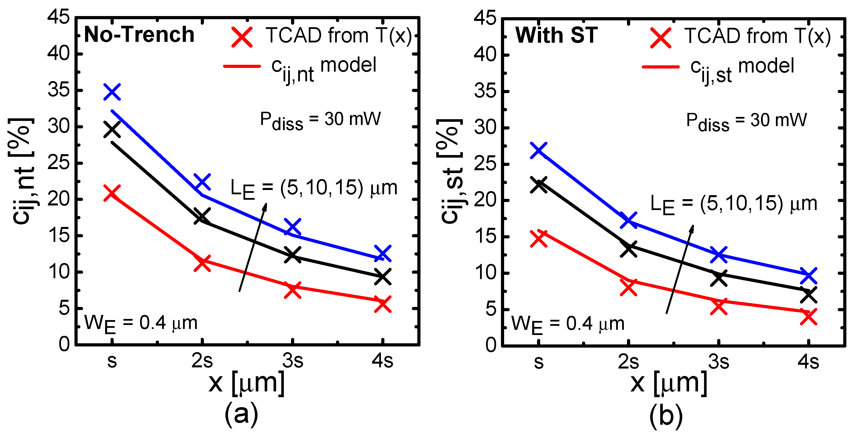
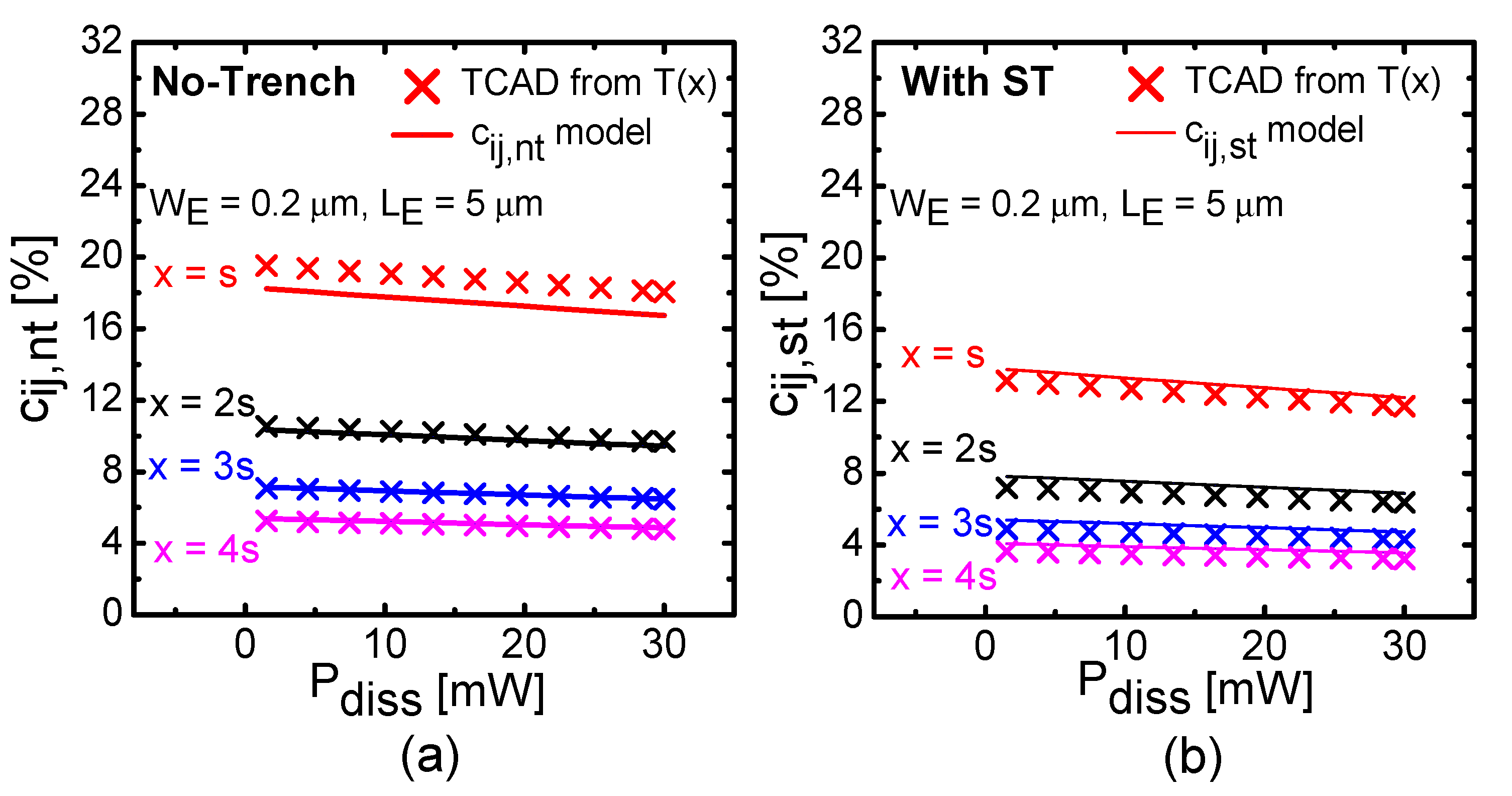
3. TCAD Simulation and Model Testing

We carried out the 3D TCAD simulation of multifinger structures based on the STMicroelectronics B55 process [13] with intrinsic Si as the substrate. Since the previous studies [1,9] demonstrated that major contribution of BEOL thermal resistance comes from metal level-1 (M1), we simulated the TCAD structure only until M1 in BEOL.
Following the modeling approach elaborated in part-I [11], prior to estimating c i j of the device with shallow trench (ST) and deep trench (DT), one needs to obtain the values of self-heating junction temperature and coupling factors of structures with no-trench and with only ST. Therefore for model testing, three TCAD structures including BEOL were prepared: (i) the first one included no-trench isolation, (ii) the second one had only ST and (iii) the third one had both ST and DT. From the simulation results of T j j and R T H , j j we extracted R T H m for each device following the methodology of [18]. Note that unlike the multifinger device being investigated here, the work in [18] dealt with only single-finger transistor. Although a multifinger transistor has a provision of creating multiple (upward as well as downward) heat-flow paths via different fingers especially when all fingers are not simultaneously heating, considering all these possibilities will lead to a more complicated model. Instead, in order to keep the model simple and suitable for implementation, we attempt to formulate and extract an effective R T H m from the single-finger self-heating characteristics (assuming one finger heating at a time in the multifinger structure) following the work of [18]. It was found that the effective R T H m values extracted for all the three devices were almost same (20 kK/W). Therefore, we assumed a constant value of R T H m for all the three types of devices under investigation. However, the value of b obtained from (3) was unique for each device due to differences in their FEOL structure. These values of b were denoted as b n t , b s t , and b d t for the structures with no-trenches, with only ST, and with both ST and DT, respectively.
For the no-trench structure, we used θ = 48 ° for the trapezoidal thermal spread as illustrated in [11]. The estimated value of b n t was then substituted in (4) to obtain the depth-dependent substrate temperature profile ( T n t ( z ) ). Subsequently we calculated the junction temperature rise Δ T j j , n t = T n t ( z = 0 ) T a m b . Figure 2 compares the difference in temperature profile along z- and x-directions, normalized by T j j , for the no-trench isolated structures with and without BEOL. It is evident that obtaining c i j using T ( z ) was as accurate as obtaining c i j from T ( x ) even in the presence of BEOL. The plot is shown in the region of interest of thermal coupling between the heat source and x , z = 4 s , where s = 2.5 μ m is the finger spacing (following STMicroelectronics B55 technology). A slight difference between the plots near the heat source essentially originated from slightly higher T ( x = s ) than T ( z = s ) possibly due to additional coupling through BEOL. It is also evident that such a difference was not visible near any of the sensing fingers, x = s to x = 4 s . Therefore, for the chosen finger-spacing ( s = 2.5 μ m) corresponding to STMicroelectronics B55 technology, we could ignore any additional coupling via BEOL and could obtain the temperature rise at a sensing finger as Δ T i j , n t = T n t ( z = | i j | s ) T a m b even in the presence of BEOL. Subsequently, we estimated the coupling factor c i j , n t = Δ T i j , n t / Δ T j j , n t . For the shallow trench isolated device, first we estimated the ambient temperature-dependent FEOL thermal resistance ( R T H s , s t ( T a m b ) ) by considering appropriate thermal spreading angles ( 35 ° within shallow trenches and 48 ° outside trenches) as illustrated in part-I [11]. Using the already extracted value of R T H m and newly estimated R T H s , s t ( T a m b ) , we estimated b s t following (3). Formulation (4) was employed appropriately starting from the bottom of the thermal spread with T r e f = T a m b to estimate Δ T j j , s t = T s t ( z = 0 ) T a m b . Subsequently the thermal resistance was calculated following R T H , j j , s t = Δ T j j , s t / P d i s s . The calculated values of Δ T j j , s t , c i j , n t and Δ T j j , n t were used to obtain c i j , s t as illustrated in (8) of [11]. Similarly for the structure with ST and DT isolation, we estimated f G considering appropriate thermal spreading angles of 35 ° and 48 ° and we estimated b d t from (3) with R T H s , d t ( T a m b ) and the already obtained value of R T H m . Afterwards we use (4) to estimate Δ T j j , d t and R T H , j j , d t . Eventually the coupling factor c i j , d t was estimated using (9) with (10) of [11] where already calculated values of c i j , s t and Δ T j j , s t were used.
Figure 3a compares the proposed self-heating model (4) and the TCAD results of junction temperature-dependent total thermal resistance for the three types of TCAD simulated structures. The comparison was done for a fixed emitter area of A E = 0.2 × 5 μ m 2 across all the three structures. Excellent model agreement was observed with the TCAD simulated data for all three structures. The extracted value of R T H m for the devices was 20 kK/W. It is important to note that only for the structure with DT, T j j and R T H , j j results could vary depending on the heating finger location due to asymmetric heat confinement among various fingers. An increase in overall temperature and thermal resistance was observed when the heating finger was located close to DT due to heat confinement as illustrated with the help of 1st and 3rd finger heating. This effect was accurately captured by the proposed model.
Figure 3b compares the c i j values obtained using TCAD simulations (symbols) and the proposed model (lines) for A E = 0.2 × 5 μ m 2 across all the three structures at a P d i s s = 30 mW. As expected, sensing fingers closer to the heat source exhibited higher coupling factors. Although Δ T j j , s t > Δ T j j , n t , one can see that c i j , s t < c i j , n t due to the fact that Δ T i j , s t Δ T i j , n t . Besides, the effect of DT confinement resulted in increased sensing finger temperature when compared with ST only structure yielding c i j , d t > c i j , s t . Note that dashed lines correspond to the case when the actual TCAD values of the ratio Δ T i j , n t / Δ T i j , s t were used in c i j , s t and c i j , d t calculation, whereas the solid lines were obtained by considering the ratio to be unity. A good level of model agreement was observed across all the structures even under the assumption of Δ T i j , n t / Δ T i j , s t = 1 . Therefore in the rest of the paper, we assume Δ T i j , n t / Δ T i j , s t = 1 for the calculations of c i j , s t and c i j , d t .
We tested the scalability of our model with the TCAD simulations of structures with different A E . Figure 4a,b and Figure 5 compare, respectively, c i j , n t , c i j , s t and c i j , d t obtained from the proposed model (lines) against the TCAD results (symbols) for devices with varying L E (in μ m) = 5 , 10 , 15 at a fixed W E = 0.4 μ m and P d i s s = 30 mW. Excellent model agreement was observed across all the devices. As expected, the amount of coupling increased with an increase in emitter length. Finally, we present the variation of c i j with electrical power dissipation at different sensing fingers in Figure 6 and Figure 7 for the three types of devices with A E = 0.2 × 5 μ m 2 . Note that in Figure 7, c i j , d t is shown for finger-2 and finger-3 heating in (a) and (b), respectively. A good level of model agreement was observed between the proposed model (lines) and TCAD simulation results (symbols) in all the cases. From the TCAD validation results presented so far, it is evident that the proposed model accurately captured the thermal coupling in different configurations of multifinger transistors with no trenches, with only ST, and with ST and DT. The accuracy of the calculated thermal coupling coefficients was consistent irrespective of the finger spacing, operating power, and emitter dimensions.

4. Model Validation with Measurements

Here we compare our self-heating and intra-device thermal coupling model with on-wafer measurement results of trench-isolated multifinger HBTs from two different state-of-the-art technologies of IHP [22] and STMicroelectronics [23].

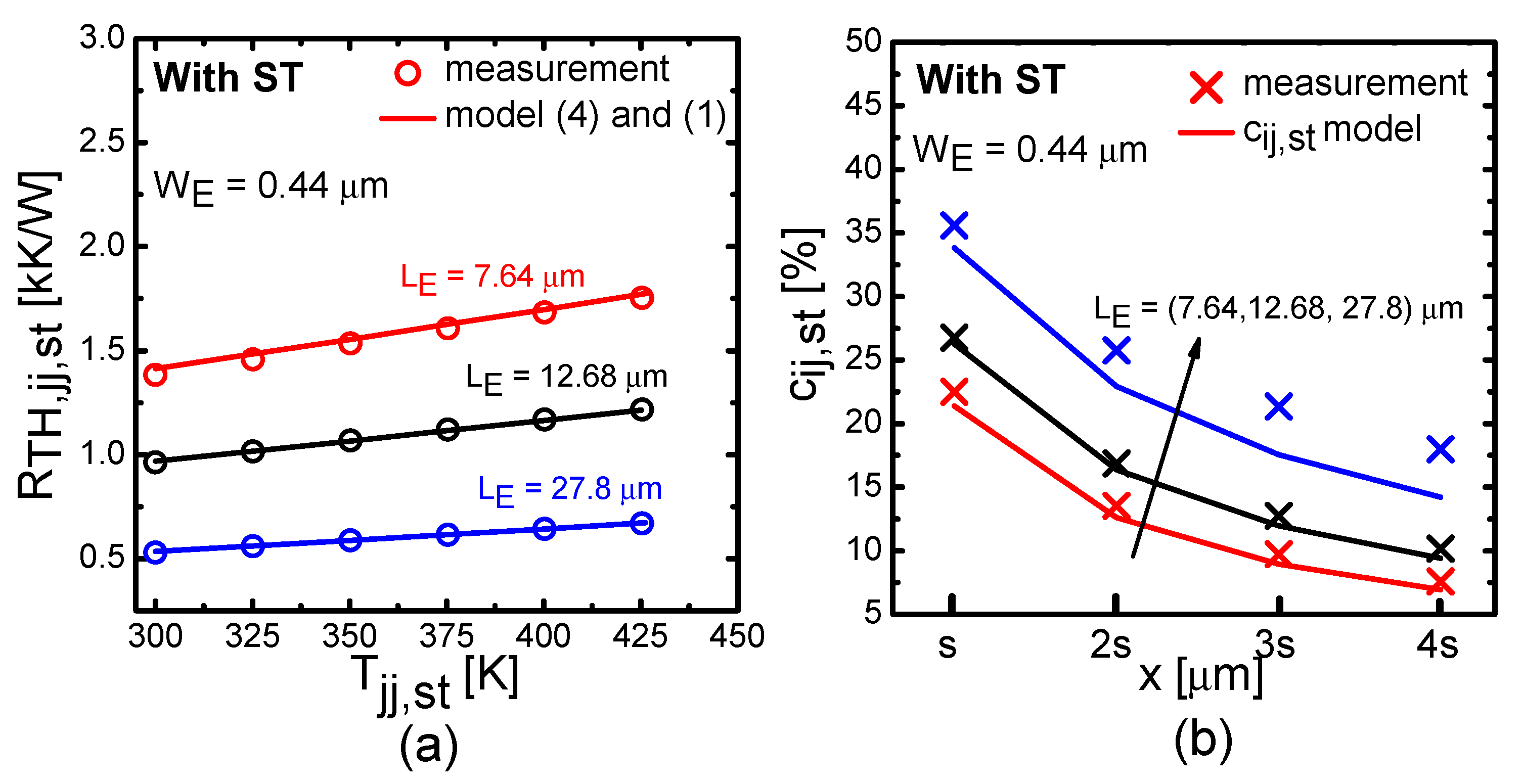
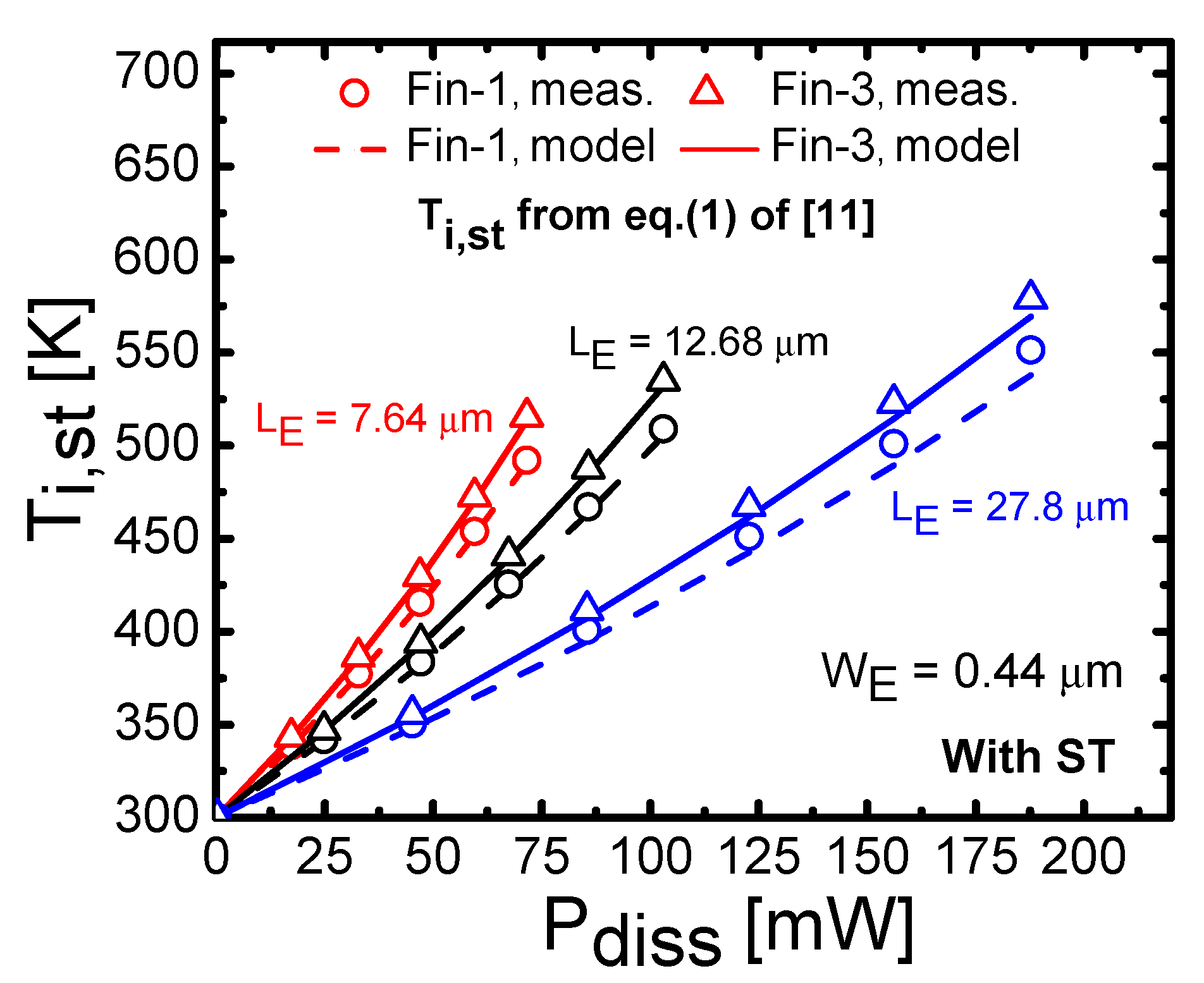
4.1. Structure with Only Shallow Trench

The recently reported work in [22] dealt with five-finger structures of an SiGe HBT process of IHP, having only shallow trench isolation. Measurement was carried out mainly for three structures with emitter dimensions of W E × L E = 0.44 × [ 7.64 , 12.68 , 27.8 ] μ m 2 . As detailed in part-I [11], prior to estimating the junction temperature and coupling factors of any trench isolated structure, we needed to analyze a comparable structure without any trenches. We started with extracting the values of R T H m for all three emitter geometries employing the extraction strategy of [18] over the measured R T H , j j , s t vs. T j j , s t data. Subsequently the coefficients of thermal conductivity model, κ a , κ b and κ c , were also optimized. These parameters were used in (4) along with the appropriate values of b n t and b s t to calculate Δ T j j , n t , c i j , n t and eventually, Δ T j j , s t . Finally c i j , s t was estimated using (8) of [11].
Figure 8a shows excellent model agreements with measured results of self-heating junction temperature-dependent thermal resistance for shallow trench isolated structures at a fixed W E and varying L E . In Figure 8b we compare the results of the proposed thermal coupling model (lines) against measurements (symbols) at different sensing fingers for the chosen devices. Excellent model agreement reflects the scalable nature of the proposed self-heating and thermal coupling model. Results shown in the figures were obtained using the optimized values of κ a = 0.118 × 10 2 mK/W, κ b = 1.195 × 10 5 m/W and κ c = 2.797 × 10 8 m/KW in (4). The values of extracted R T H m used in the model are 20 , 15 , 12 kK/W in the order of increasing L E .

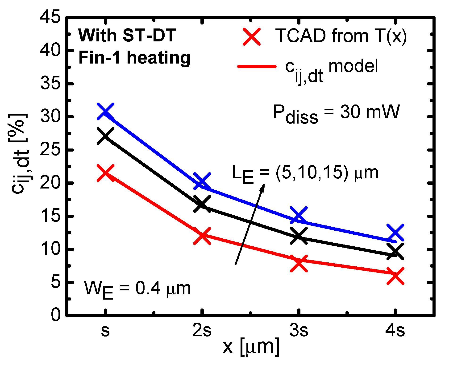
4.2. Structure with Shallow and Deep Trench

A study was conducted in [23] to investigate the thermal coupling effect in SiGe:C multifinger structure having shallow and deep trench isolation from the STMicroelectronics B5T process.
Measurements were carried out for a five finger transistor with A E = 0.18 × 5 μ m 2 . First we extracted the appropriate BEOL R T H m and b d t using the self heating data of R T H , j j , d t vs. T j j , d t for the case when the 4th finger was only heating. Subsequently values of κ a , κ b and κ c were optimized. These parameter values were used in (4) along with the estimated values of b n t and b s t to estimate Δ T j j , n t , c i j , n t , Δ T j j , s t and c i j , s t . Finally similar quantities of the structure with only ST were used in the model of c i j , d t along with the estimated value of Δ T j j , d t obtained using (4). In Figure 9a, total thermal resistance R T H , j j , d t obtained from the model was compared against the corresponding measurement data. Excellent model agreement with the experimental data for the junction temperature at different P d i s s was observed. Figure 9b shows the model agreement with experimental data achieved using the c i j , d t model. An optimized ratio value of Δ T i j , d t / Δ T i j , s t = 2.03 was used to calculate c i j , d t for the chosen device. The demonstrated results were obtained after employing optimized values of κ a = 0.83 × 10 2 mK/W, κ b = 9.76 × 10 8 m/W and κ c = 9.83 × 10 9 m/KW. Excellent model agreements for both self-heating and thermal coupling measurement data of the structures with only ST and with ST and DT irrespective of the operating power and emitter geometry variation highlight, respectively, the robustness and scalability of the proposed model.
Finally Figure 10 presents the total finger temperature if the measured data for self-heating and thermal coupling temperatures for each device were directly superposed following (1) from [11]. We also compared the corresponding modeling results showing excellent correlation. It is understood that the superposition of these two temperatures was not valid as temperature-dependent κ of Si was automatically considered in any measurement causing the original heat diffusion equation to be nonlinear which could not allow the superposition principle. However, as demonstrated in [11] with the help of TCAD data, the difference with the true finger temperature was not significant. Since there was no fool-proof method so far reported in the literature to determine the true finger temperature in a multifinger device when all fingers are heating simultaneously, we present the limited model comparison. It is apparent that both the measurement as well as modeling framework need further improvement to investigate the true temperatures of all the fingers in any multifinger transistor structure.

5. Conclusions

In this part we extend the already developed physics based scalable model of part-I [11] for the depth-dependent substrate temperature including the effect of BEOL heat flow by introducing only one additional parameter. We also present the extraction technique for this new parameter. This extended model is tested against the TCAD simulated data that include the BEOL effect. Finally the model is validated with the experimental data for the multifinger structures with only ST and with ST and DT isolation fabricated following two state-of-the-art SiGe HBT processes. The model shows excellent agreement with TCAD simulation and measurement data for various emitter finger geometries demonstrating its overall utility.

Author Contributions

Conceptualization, A.G., S.B. and A.C.; methodology, S.B. and A.C.; software, A.G., K.N. and S.B.; validation, A.G. and K.N.; formal analysis, A.G., K.N.; investigation, A.G.; resources, S.Y., S.F. and T.Z.; writing—original draft preparation, A.C.; writing—review and editing, S.B., S.F. and T.Z.; visualization, A.G., K.N., S.B. and A.C.; supervision, S.B. and A.C.; project administration, A.C.; funding acquisition, A.C., S.F. and T.Z. All authors have read and agreed to the published version of the manuscript.

Funding

This work was supported in part by the EU under Project Taranto under Grant 737454, in part by ISRO project ELE/17-18/176/ISRO/ANJA and in part by DST, India, under Project EMR/2016/004726.

Conflicts of Interest

The authors declare no conflict of interest.

References

  1. Sahoo, A.K.; Fregonese, S.; Weis, M.; Maneux, C.; Malbert, N.; Zimmer, T. Impact of back-end-of-line on thermal impedance in SiGe HBTs. In Proceedings of the International Conference on Simulation of Semiconductor Processes and Devices (SISPAD), Glasgow, UK, 3–5 September 2013; pp. 188–191. [Google Scholar]
  2. Magnani, A.; Sasso, G.; d’Alessandro, V.; Codecasa, L.; Rinaldi, N.; Aufinger, K. Advanced thermal resistance simulation of SiGe HBTs including backend cooling effect. In Proceedings of the International Workshop on Thermal Investigations of ICs and Systems (THERMINIC), Paris, France, 30 September–2 October 2015; pp. 1–5. [Google Scholar]
  3. Sahoo, A.K.; Fregonese, S.; Weiss, M.; Maneux, C.; Zimmer, T. A Scalable Model for Temperature Dependent Thermal Resistance of SiGe HBTs. In Proceedings of the Bipolar/BiCMOS Circuits and Technology Meeting (BCTM), Bordeaux, France, 30 September–3 October 2013; pp. 29–32. [Google Scholar] [CrossRef]
  4. Walkey, D.J.; Smy, T.J.; Marchesan, D.; Tran, H.; Schröter, M. A scalable thermal model for trench isolated bipolar devices. Solid-State Electron 2000, 44, 1373–1379. [Google Scholar] [CrossRef]
  5. Rieh, J.S.; Greenberg, D.; Liu, Q.; Joseph, A.J.; Freeman, G.; Ahlgren, D.C. Structure optimization of trench-isolated SiGe HBTs for simultaneous improvements in thermal and electrical performances. IEEE Trans. Electron Dev. 2005, 52, 2744–2752. [Google Scholar] [CrossRef]
  6. Chakravorty, A.; D’Esposito, R.; Balanethiram, S.; Frégonèse, S.; Zimmer, T. Analytic Estimation of Thermal Resistance in HBTs. IEEE Trans. Electron Dev. 2016, 63, 2994–2998. [Google Scholar] [CrossRef]
  7. Sahoo, A.K.; Fregonese, S.; Desposito, R.; Aufinger, K.; Maneux, C.; Zimmer, T. A geometry scalable model for nonlinear thermal impedance of trench isolated HBTs. IEEE Electron Dev. Lett. 2015, 36, 56–58. [Google Scholar] [CrossRef]
  8. D’Esposito, R.; Frégonèse, S.; Chakravorty, A.; Chevalier, P.; Céli, D.; Zimmer, T. Innovative SiGe HBT Topologies With Improved Electrothermal Behavior. IEEE Trans. Electron Dev. 2016, 63, 2677–2683. [Google Scholar] [CrossRef] [Green Version]
  9. D’Esposito, R.; Frégonèse, S.; Zimmer, T.; Chakravorty, A. Dedicated test-structures for investigation of the thermal impact of the BEOL in advanced SiGe HBTs in time and frequency domain. In Proceedings of the International Conference on Microelectronic Test Structures (ICMTS), Yokohama, Japan, 28–31 March 2016; pp. 28–31. [Google Scholar] [CrossRef]
  10. Dwivedi, A.; Chakravorty, A.; D’Esposito, R.; Sahoo, A.K.; Fregonese, S.; Zimmer, T. Effects of BEOL on self-heating and thermal coupling in SiGe multi-finger HBTs under real operating condition. Solid-State Electron 2016, 115, 1–6. [Google Scholar] [CrossRef]
  11. Gupta, A.; Nidhin, K.; Balanethiram, S.; Yadav, S.; Chakravorty, A.; Fregonese, S.; Zimmer, T. Static Thermal Coupling Factors in Multi-Finger Bipolar Transistors: Part I-Model Development. J. Electron. 2020, 9, 1333. [Google Scholar] [CrossRef]
  12. Balanethiram, S.; Chakravorty, A.; D’Esposito, R.; Fregonese, S.; Céli, D.; Zimmer, T. Accurate modeling of thermal resistance for on-wafer SiGe HBTs using average thermal conductivity. IEEE Trans. Electron Dev. 2017, 64, 3955–3960. [Google Scholar] [CrossRef] [Green Version]
  13. Chevalier, P.; Avenier, G.; Ribes, G.; Montagné, A.; Canderle, E.; Céli, D.; Derrier, N.; Deglise, C.; Durand, C.; Quémerais, T.; et al. A 55 nm triple gate oxide 9 metal layers SiGe BiCMOS technology featuring 320 GHz fT/370 GHz fmax HBT and high-Q millimeter-wave passives. In Proceedings of the 2014 IEEE International Electron Devices Meeting, San Francisco, CA, USA, 15–17 December 2014. [Google Scholar]
  14. Balanethiram, S.; Chakravorty, A.; D’Esposito, R.; Fregonese, S.; Zimmer, T. An improved scalable self-consistent iterative model for thermal resistance in SiGe HBTs. In Proceedings of the Bipolar/BiCMOS Circuits and Technology Meeting (BCTM), New Brunswick, NJ, USA, 25–27 September 2016; pp. 150–153. [Google Scholar] [CrossRef] [Green Version]
  15. Gao, G.B.; Ünlü, M.S.; Morkoc, H.; Blackburn, D.L. Emitter ballasting resistor design for, and current handling capability of AlGaAs/GaAs power heterojunction bipolar transistors. IEEE Trans. Electron Dev. 1991, 38, 185–196. [Google Scholar] [CrossRef]
  16. Synopsys, Inc. Sentaurus: Sentaurus Device User Guide; Release H-2013.03; Synopsys, Inc.: Mountain View, CA, USA, 2013. [Google Scholar]
  17. D’Esposito, R. Electro-Thermal Characterization, TCAD Simulations and Compact Modeling of Advanced SiGe HBTs at Device and Circuit Level. Ph.D. Thesis, University of Bordeaux, Talence, France, 2016. [Google Scholar]
  18. Balanethiram, S.; D’Esposito, R.; Chakravorty, A.; Fregonese, S.; Zimmer, T. Extraction of BEOL Contributions for Thermal Resistance in SiGe HBTs. IEEE Trans. Electron Dev. 2017, 64, 1380–1384. [Google Scholar] [CrossRef] [Green Version]
  19. Slack, G.A. Thermal conductivity of pure and impure silicon, silicon carbide, and diamond. J. Appl. Phys. 1964, 35, 3460–3466. [Google Scholar] [CrossRef]
  20. Lee, Y.; Hwang, G.S. Mechanism of thermal conductivity suppression in doped silicon studied with nonequilibrium molecular dynamics. Phys. Rev. B 2012, 86, 075202. [Google Scholar] [CrossRef] [Green Version]
  21. Nghiêm, T.T.; Saint-Martin, J.; Dollfus, P. Electro-thermal simulation based on coupled Boltzmann transport equations for electrons and phonons. J. Comput. Electron. 2016, 15, 3–15. [Google Scholar] [CrossRef] [Green Version]
  22. Lehmann, S.; Zimmermann, Y.; Pawlak, A.; Schroter, M. Characterization of the static thermal coupling between emitter fingers of bipolar transistors. IEEE Trans. Electron Dev. 2014, 61, 3676–3683. [Google Scholar] [CrossRef]
  23. Weiss, M.; Sahoo, A.K.; Maneux, C.; Fregonese, S.; Zimmer, T. Mutual thermal coupling in SiGe:C HBTs. In Proceedings of the Symposium on Microelectronics Technology and Devices (SBMicro), Curitiba, Brazil, 2–6 September 2013; pp. 1–4. [Google Scholar] [CrossRef]
Figure 1. 3D cross-sectional view of a five-finger TCAD structure of STMicroelectronics B55 process [13] containing shallow and deep trenches along with the eight metal layers (M1 to M8). A closer view of the corner finger is shown at the inset with emitter (E), base (B), and collector (C) contacts, and the heat source (HS).
Electronics 09 01365 g001
Figure 2. A comparison between the difference in T ( z ) and T ( x ) from TCAD, normalized with the rise in peak junction temperature Δ T j j , for the structures with and without back-end-of-line (BEOL) heat flow.
Electronics 09 01365 g002
Figure 3. (a) T j j dependent R T H , j j variation and (b) c i j at the sensing fingers: A comparison between TCAD results (symbols) and the proposed model (lines) for the three types of structures with A E = 0.2 × 5 μ m 2 and P d i s s = 30 mW. Solid lines in (b) correspond to the case when Δ T i j , n t / Δ T i j , s t = 1 in c i j , s t and c i j , d t model. Here finger spacing s = 2.5 μ m.
Electronics 09 01365 g003
Figure 4. A comparison between the TCAD results and the proposed model of (a) c i j , n t and (b) c i j , s t for devices with different L E at a fixed W E = 0.4 μ m and P d i s s = 30 mW.
Electronics 09 01365 g004
Figure 5. Values of c i j , d t at the sensing fingers for variation in L E at a fixed W E = 0.4 μ m and P d i s s = 30 mW: A comparison between TCAD results (symbols) and the proposed model (lines) in (9) and (10) of [11].
Electronics 09 01365 g005
Figure 6. Dissipated power dependent (a) c i j , n t and (b) c i j , s t at different sensing fingers for a structures with A E = 0.2 × 5 μ m 2 : A comparison between the proposed model and TCAD simulation results.
Electronics 09 01365 g006
Figure 7. P d i s s —dependent c i j , d t at different sensing fingers when (a) 2nd and (b) 3rd fingers are heating individually in a five-finger device with A E = 0.2 × 5 μ m 2 .
Electronics 09 01365 g007
Figure 8. (a) T j j , s t dependent R T H , j j , s t and (b) c i j , s t at different sensing fingers: A comparison between the proposed model (lines) and measurements (symbols) [22] for devices with varying L E at a fixed W E . Here finger spacing s = 3.23 μ m.
Electronics 09 01365 g008
Figure 9. (a) T j j , d t —dependent R T H , j j , d t and (b) c i j , d t at different sensing fingers: A comparison between the proposed model (lines) and measurements (symbols) [23] for a device with A E = 0.18 × 5 μ m 2 . Δ T i j , d t / Δ T i j , s t = 2.03 was used in the model. Here finger spacing s = 5 μ m.
Electronics 09 01365 g009
Figure 10. P d i s s —dependent total junction temperature T i , s t of 1st and 3rd finger in a five-finger structure with shallow trench (ST), T i , s t is obtained after substituting values of Δ T j j , s t and c i j , s t in Equation (1) of [11]. Symbols are obtained after substituting measurement data ([22]) while the solid and dash lines results after inserting self-heating and thermal coupling model values in the equation.
Electronics 09 01365 g010

