Patch Antenna-in-Package for 5G Communications with Dual Polarization and High Isolation


Abstract
:1. Introduction
2. Antenna Design
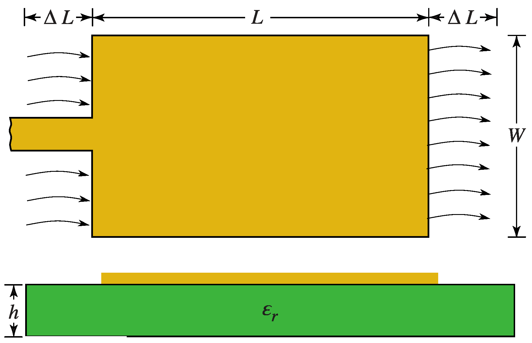
2.1. Patch Antennas
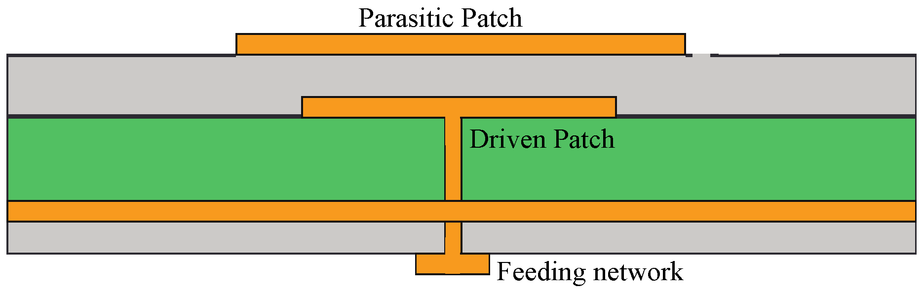
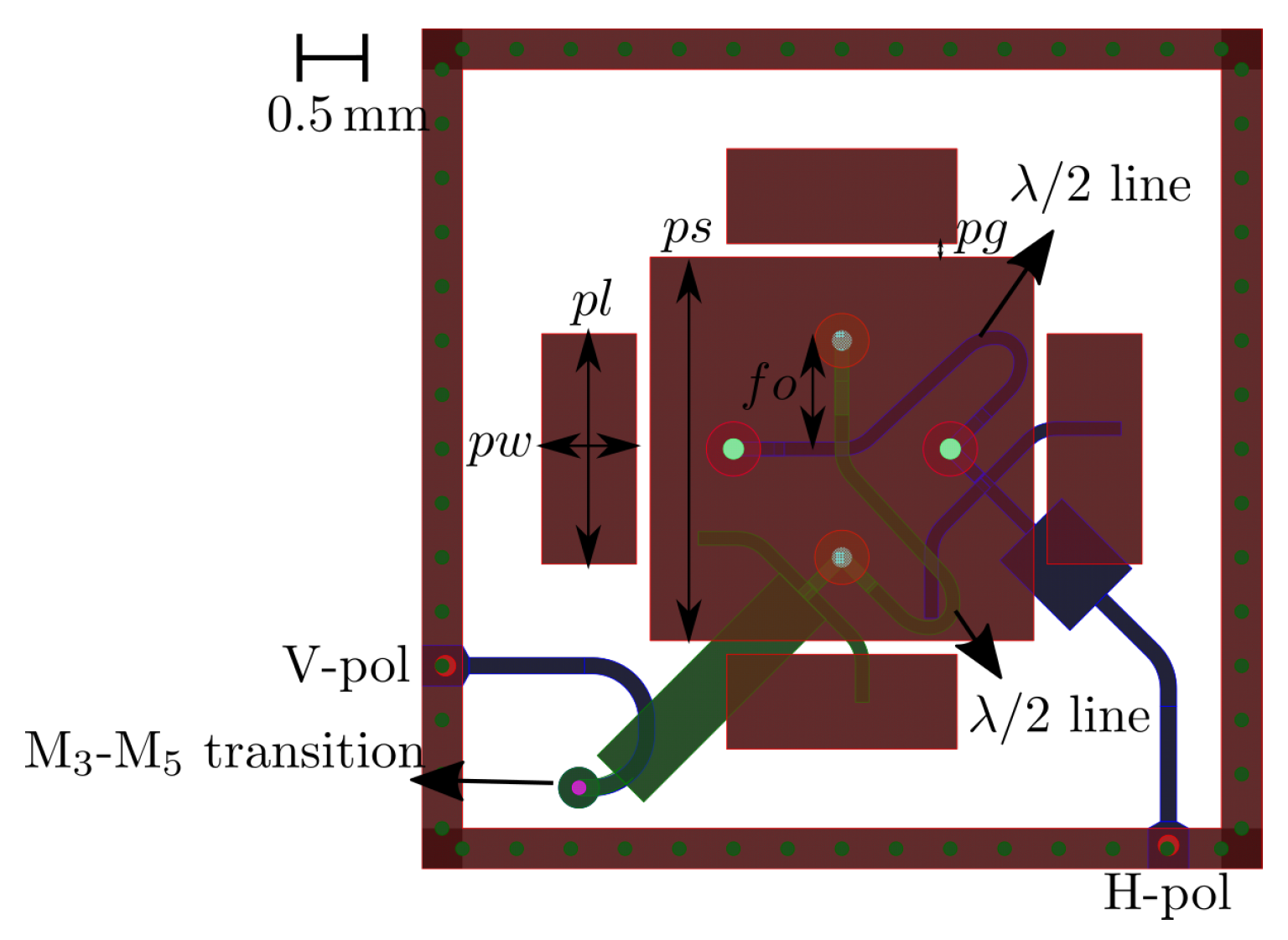
2.2. Rotationally Symmetric Patch with Parasitics
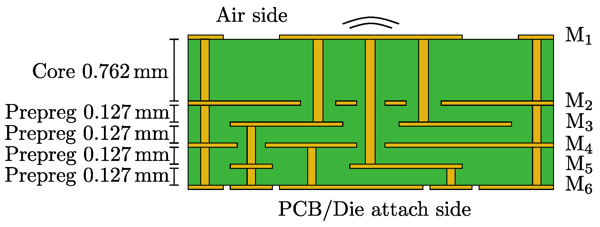
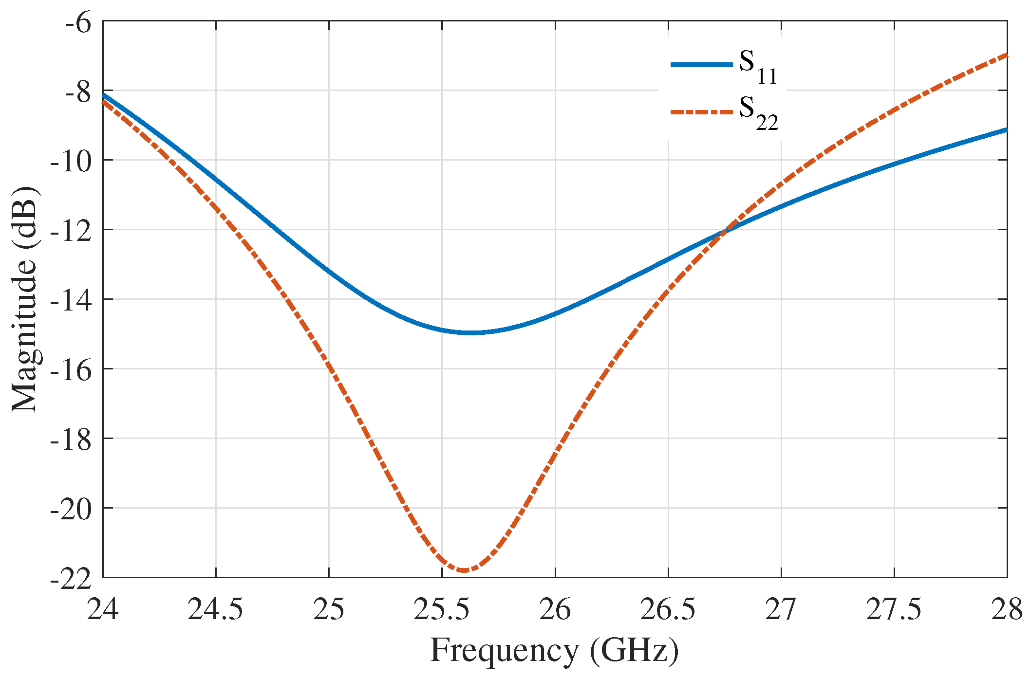
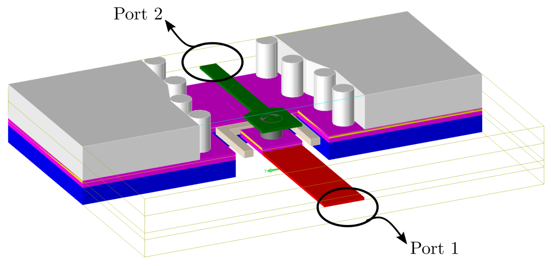
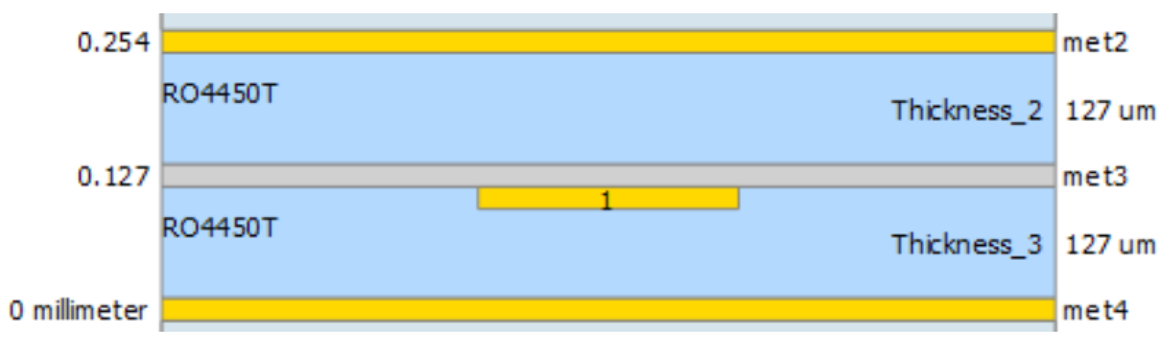
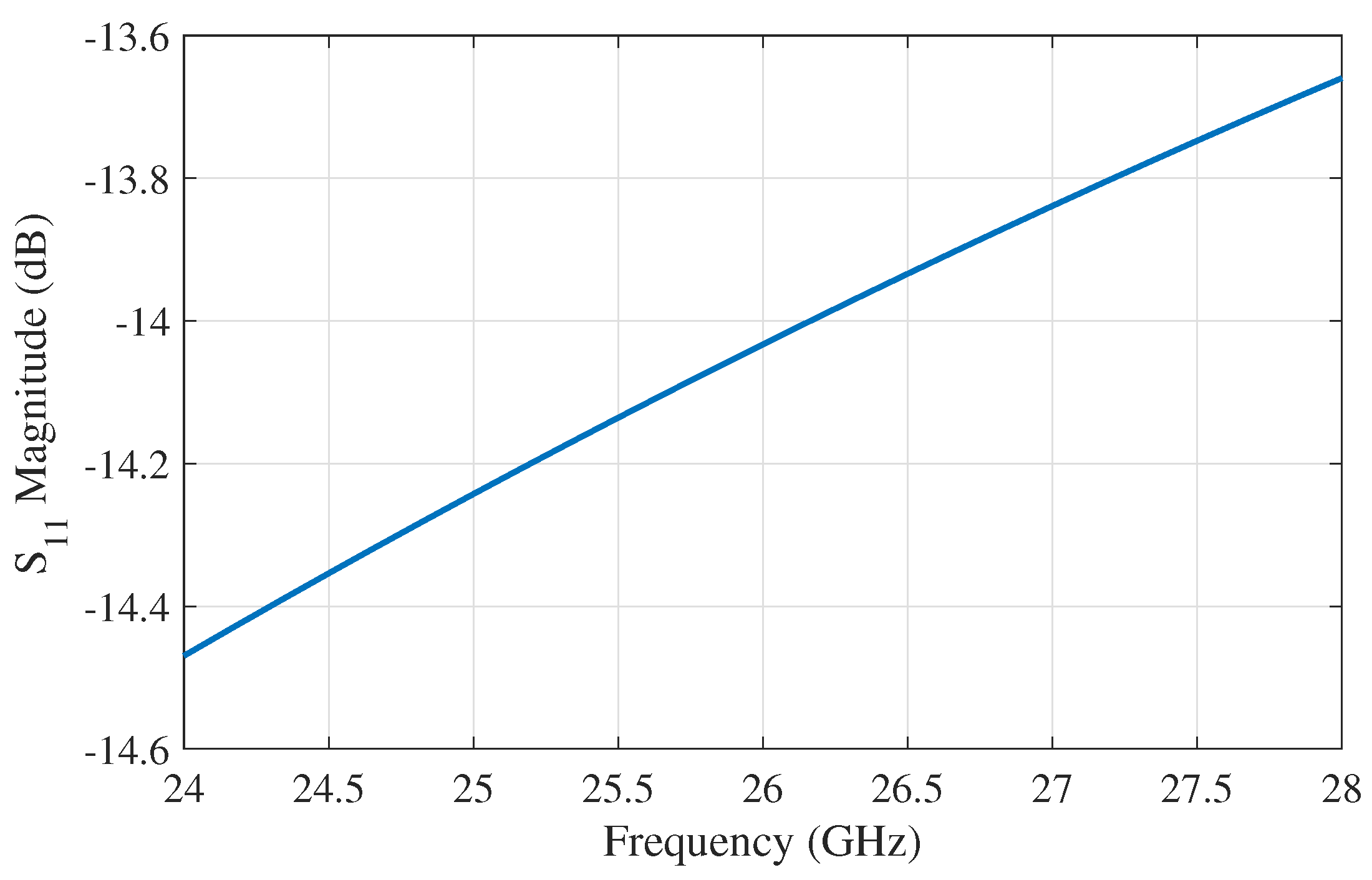
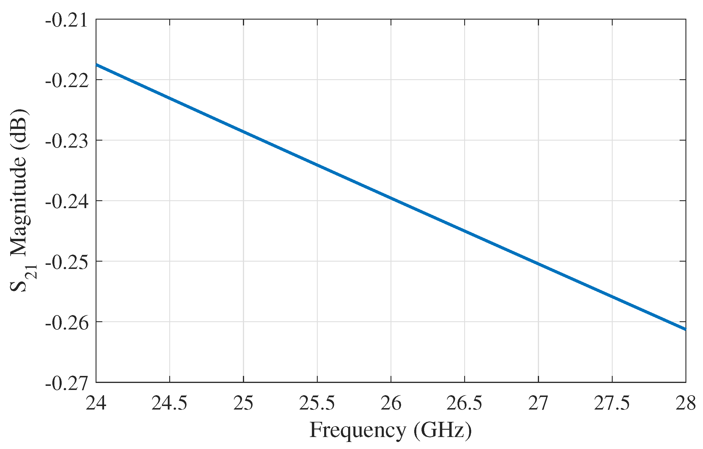
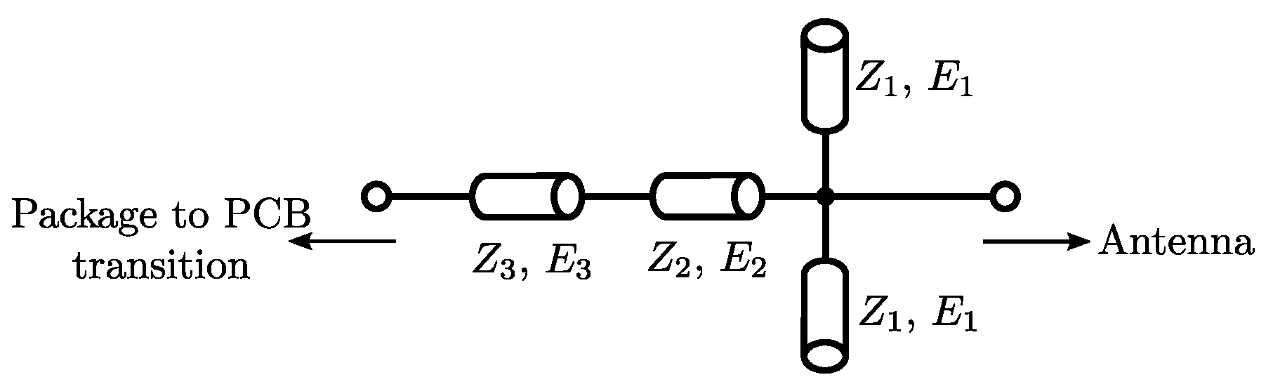
3. PCB-to-Package Transition
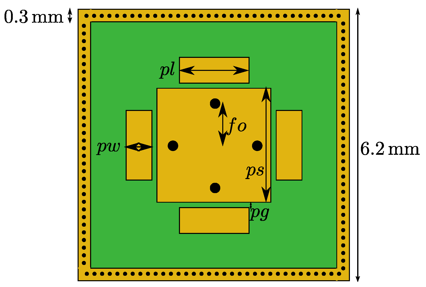
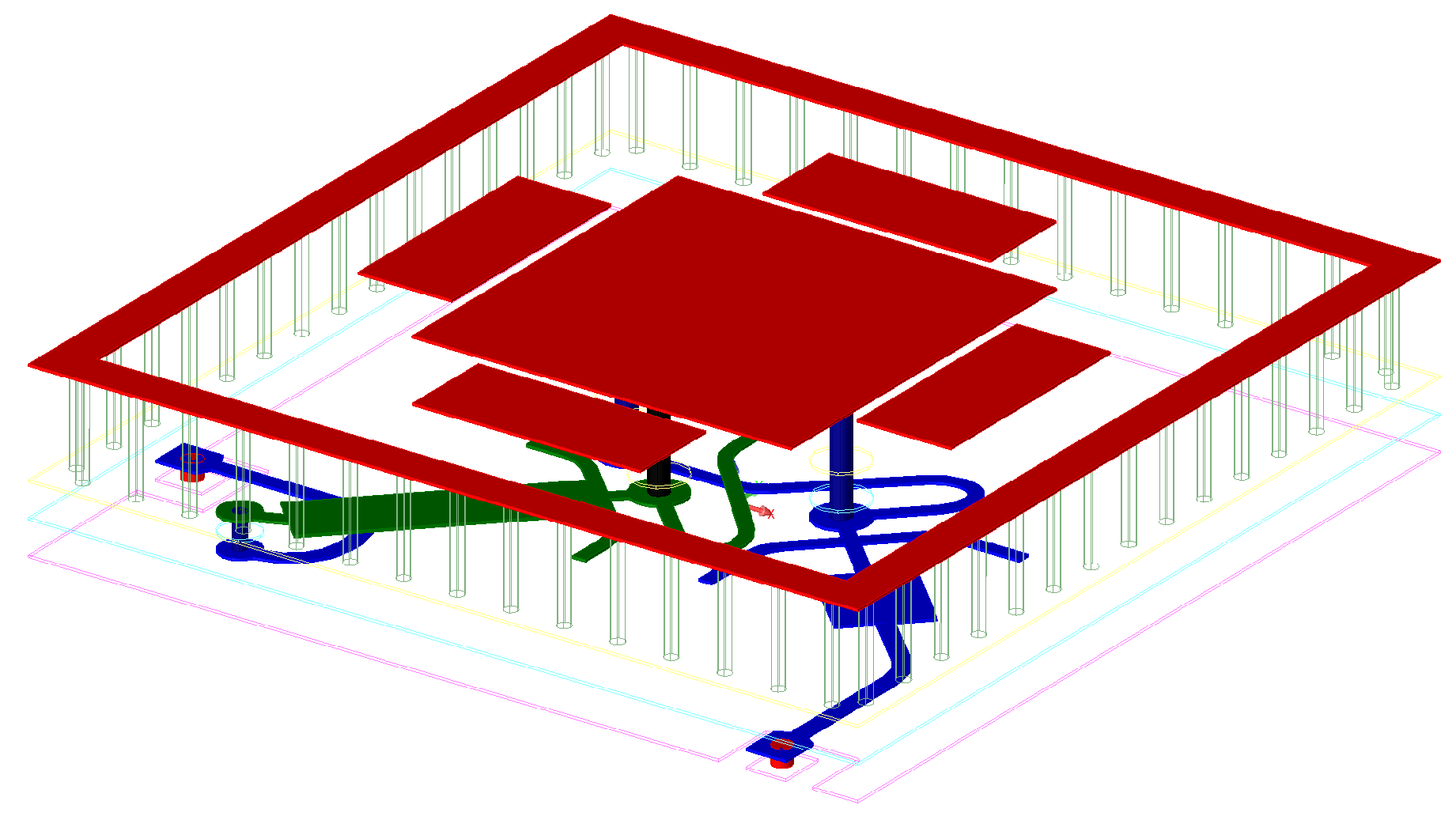
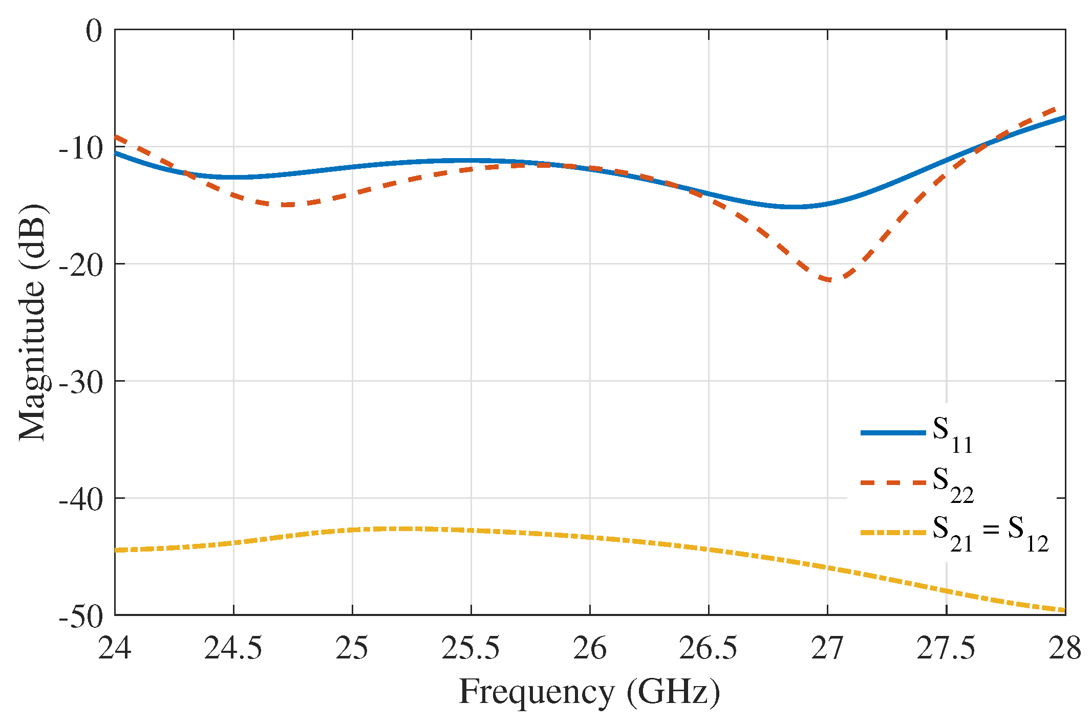
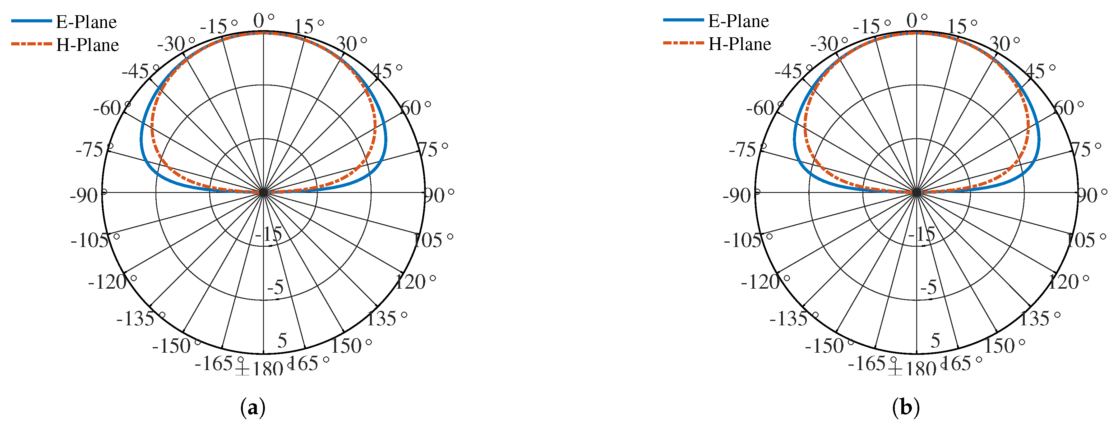
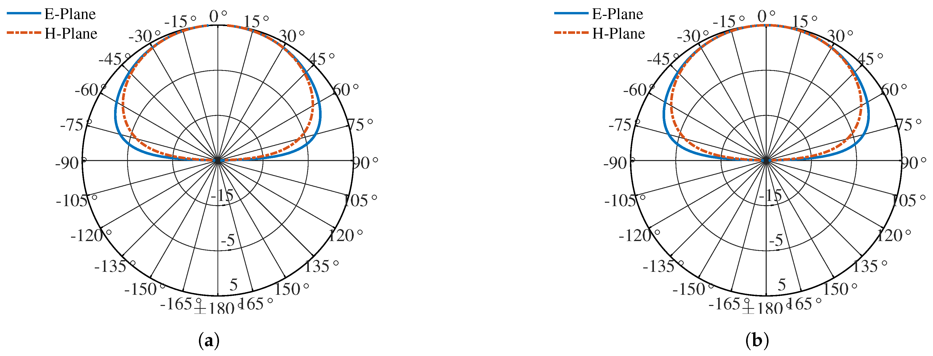
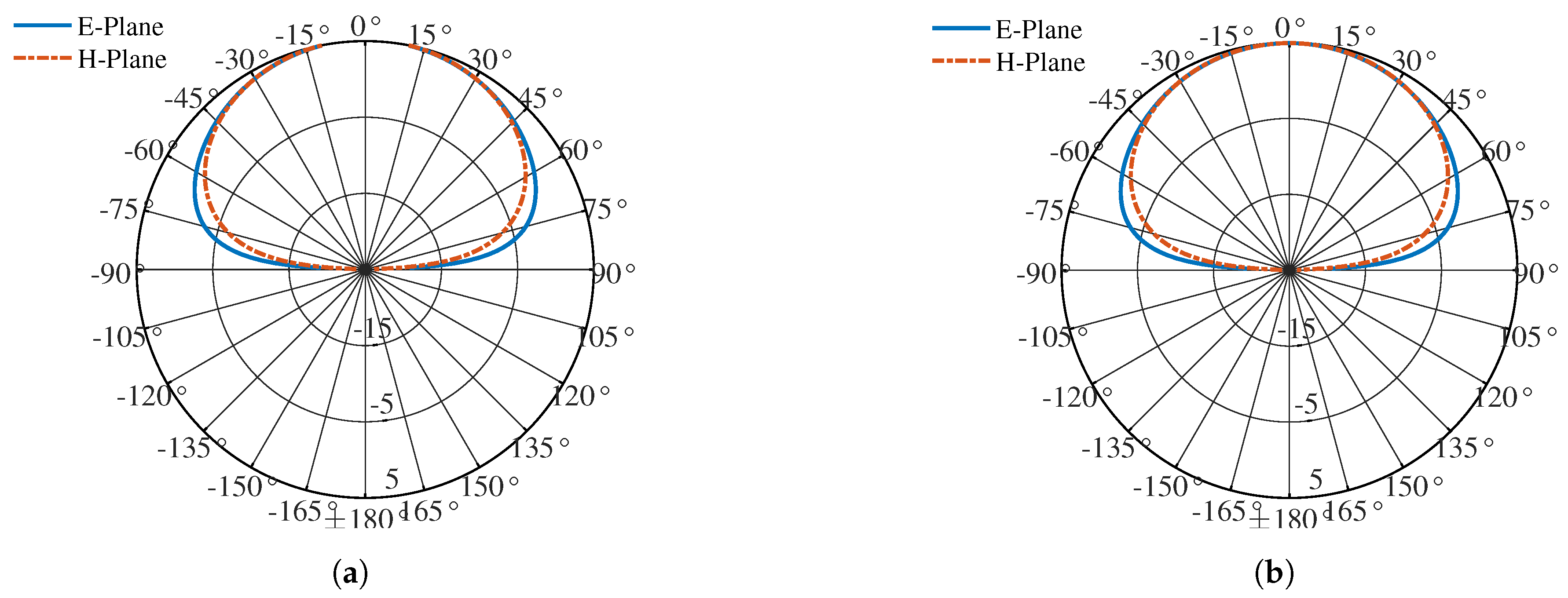
4. Final Assembly
5. Conclusions
Author Contributions
Funding
Conflicts of Interest
References
- Tjelta, T.; Temple, S.; Mohr, R.W. Euro-5G–Supporting the European 5G Initiative; EURO-5G Consortium Parties: Heidelberg, Germany, 2015. [Google Scholar]
- Balanis, C. Antenna Theory: Analysis and Design; Wiley: Hoboken, NJ, USA, 2016. [Google Scholar]
- Balanis, C.A. Modern Antenna Handbook; John Wiley & Sons: Hoboken, NJ, USA, 2011. [Google Scholar]
- Guo, G.; Wu, L.; Zhang, Y.; Mao, J. Stacked patch array in LTCC for 28 GHz antenna-in-package applications. In Proceedings of the 2017 IEEE Electrical Design of Advanced Packaging and Systems Symposium (EDAPS), Haining, China, 11–16 December 2017; pp. 1–3. [Google Scholar]
- Lu, Y.; Fang, B.; Mi, H.; Chen, K. Mm-Wave Antenna in Package (AiP) Design Applied to 5th Generation (5G) Cellular User Equipment Using Unbalanced Substrate. In Proceedings of the 2018 IEEE 68th Electronic Components and Technology Conference (ECTC), San Diego, CA, USA, 29 May–1 June 2018; pp. 208–213. [Google Scholar] [CrossRef]
- Xia, H.; Zhang, T.; Li, L.; Zheng, F. A low-cost dual-polarized 28 GHz phased array antenna for 5G communications. In Proceedings of the 2018 International Workshop on Antenna Technology (iWAT), Nanjing, China, 5–7 March 2018; pp. 1–4. [Google Scholar]
- Nawaz, H.; Tekin, I. Dual Polarized, Differential Fed Microstrip Patch Antennas with very High Inter-port Isolation for Full Duplex Communication. IEEE Trans. Antennas Propag. 2017, 65, 7355–7360. [Google Scholar] [CrossRef]
- Kumar, G.; Ray, K. Broadband Microstrip Antennas; Artech House Antennas and Propagation Library: Norwood, MA, USA, 2003. [Google Scholar]
- Mak, K.M.; Lai, H.W.; Luk, K.M. A 5G Wideband Patch Antenna with Antisymmetric L-shaped Probe Feeds. IEEE Trans. Antennas Propag. 2017, 66, 957–961. [Google Scholar] [CrossRef]
- Polyak, B. Newton’s method and its use in optimization. Eur. J. Oper. Res. 2007, 181, 1086–1096. [Google Scholar] [CrossRef]
- Pozar, D. Microwave Engineering, 4th ed.; Wiley: Hoboken, NJ, USA, 2011. [Google Scholar]
- Wu, Y.; Liu, Y.; Li, S. A Dual-Frequency Transformer for Complex Impedances with Two Unequal Sections. IEEE Microw. Wirel. Components Lett. 2009, 19, 77–79. [Google Scholar] [CrossRef]
- Marini, F.; Walczak, B. Particle swarm optimization (PSO). A tutorial. Chemom. Intell. Lab. Syst. 2015, 149, 153–165. [Google Scholar] [CrossRef]

| Polarization | ||||||
|---|---|---|---|---|---|---|
| V-Pol | ||||||
| H-Pol |
© 2020 by the authors. Licensee MDPI, Basel, Switzerland. This article is an open access article distributed under the terms and conditions of the Creative Commons Attribution (CC BY) license (http://creativecommons.org/licenses/by/4.0/).
Share and Cite
Santos, H.; Pinho, P.; Salgado, H. Patch Antenna-in-Package for 5G Communications with Dual Polarization and High Isolation. Electronics 2020, 9, 1223. https://doi.org/10.3390/electronics9081223
Santos H, Pinho P, Salgado H. Patch Antenna-in-Package for 5G Communications with Dual Polarization and High Isolation. Electronics. 2020; 9(8):1223. https://doi.org/10.3390/electronics9081223
Chicago/Turabian StyleSantos, Hugo, Pedro Pinho, and Henrique Salgado. 2020. "Patch Antenna-in-Package for 5G Communications with Dual Polarization and High Isolation" Electronics 9, no. 8: 1223. https://doi.org/10.3390/electronics9081223
APA StyleSantos, H., Pinho, P., & Salgado, H. (2020). Patch Antenna-in-Package for 5G Communications with Dual Polarization and High Isolation. Electronics, 9(8), 1223. https://doi.org/10.3390/electronics9081223