1. Introduction
The terahertz (THz) frequency range, which is from 300 GHz to 3 THz, has recently gained much attention from researchers due to its wide range of applications such as high-speed communication, imaging security system, and spectroscopy [
1,
2]. In these applications, a high power and high frequency signal source is one of the most important components to create a system with superior quality. Among the technologies for designing a signal source, CMOS technology stands out as a reliable selection to build a high-quality signal source because of its low production cost and compact size. However, CMOS signal sources present some difficulties such as low maximum oscillation frequency (
fmax) and low output power at the THz frequency range.
Though a fundamental frequency oscillator is widely adopted for generating an output signal having oscillation frequency smaller than
fmax [
3,
4,
5,
6,
7], but a fundamental frequency oscillator cannot generate a high frequency output signal that has oscillation frequency greater than
fmax. Therefore, a harmonic frequency oscillator is a viable solution to overcome the low
fmax of CMOS technology and to generate a high frequency output signal that has oscillation frequency greater than
fmax. Nevertheless, only a limited output power extracted from a single oscillator core is a problem of harmonic frequency oscillator at this high frequency range [
8,
9].
This paper proposes a THz frequency CMOS coupled stack oscillator with a good output power level. The oscillator core uses a frequency selective negative resistance (FSNR) tank to increase the negative transconductance and the transformer-based topology to minimize the loss of the second harmonic power. The push-push topology is employed to generate a high oscillation frequency over
fmax and multiple coupled oscillator cores to obtain a high output power. The proposed oscillator, implemented in a 65 nm bulk CMOS process, generates a maximum output power of −0.8 dBm at 350 GHz. In
Section 2, the proposed signal source’s structure is analyzed.
Section 3 presents the measurement setups and measurement results of the proposed oscillator. Finally,
Section 4 summarize the findings in this paper.
2. The Proposed Signal Source
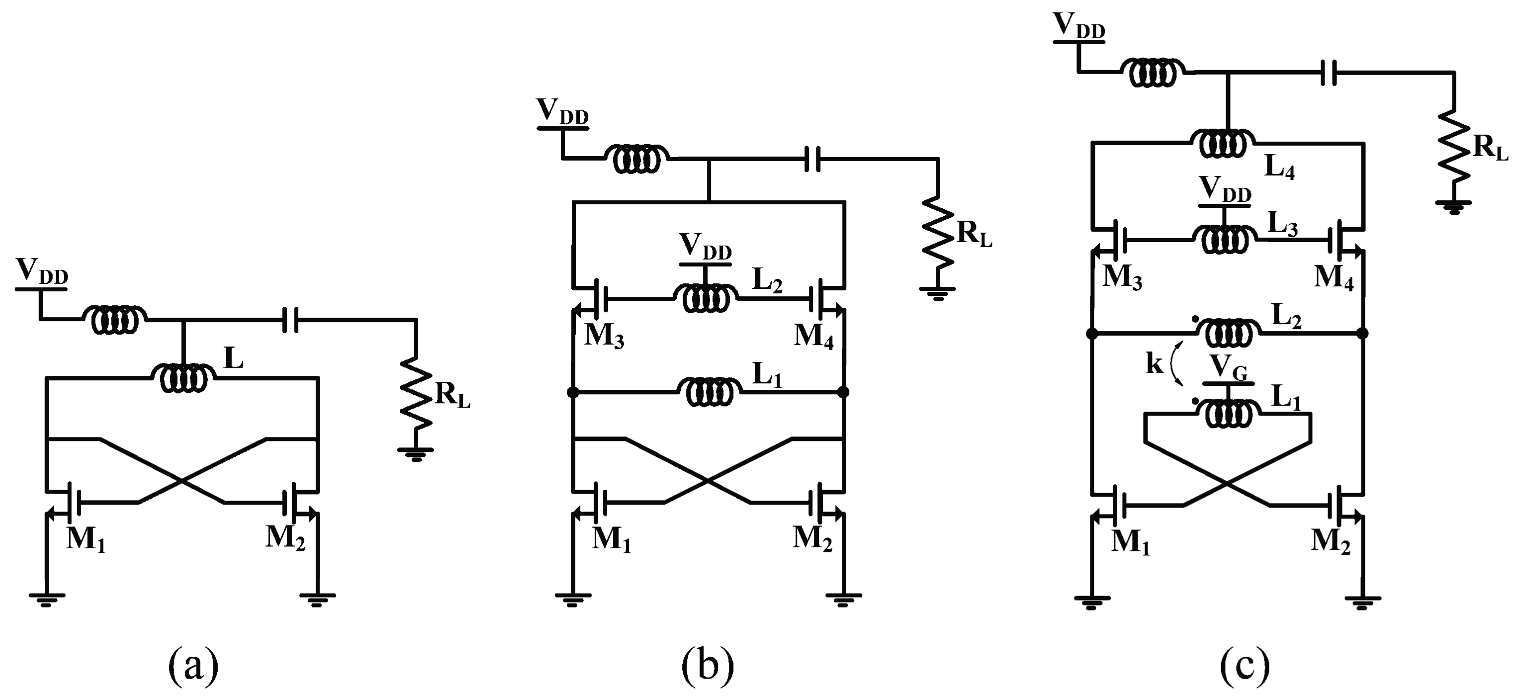
Figure 1a shows a schematic of a conventional cross coupled oscillator (XCO). At the THz frequency, a conventional XCO suffers from low negative transconductance at the fundamental frequency and high loss at the second harmonic frequency because of the direct connection of a low gate impedance of transistors M
1 and M
2 to the second harmonic output path. In
Figure 1b, a conventional stack oscillator with FSNR tank, implemented by transistors M
3, M
4, and inductor L
2, is connected in parallel with the cross-coupled pair M
1 and M
2 to boost the total negative transconductance at the fundamental frequency, so a higher output power can be generated [
2]. A novel stack oscillator, shown in
Figure 1c, is proposed to minimize the loss at the second harmonic frequency of the conventional stack oscillator by connecting a transformer between gate and drain terminals of cross-coupled pair.
Figure 2 shows circuit simulation results for a negative transconductance at 180 GHz fundamental frequency of the conventional XCO, the conventional stack oscillator, and the proposed stack oscillator. All topologies have the same of transistor size W/L of 12 μm/60 nm, and the same voltage across the drain and source terminals of each transistor of 1V. The conventional XCO generates only 2 mS negative transconductance, and conventional stack oscillator generates 11.9 mS negative transconductance due to the extra negative transconductance added by FSNR tank. The negative transconductance of the proposed stack oscillator increases from 5.8 mS to 11.6 mS with a coupling factor k increases from 0.2 to 0.9.
The effectiveness of the transformer in the proposed stack oscillator in reducing the loss of the second harmonic output power is simulated and shown in
Figure 3. In this simulation, we assume that both the conventional stack oscillator and the proposed stack oscillator generate 0 dBm power at the second harmonic frequency inside the oscillator tank. The gate impedance looking from the drain terminals of transistors in the proposed stack oscillator is increased with a decrease of the coupling factor k and increased from 3.5 Ω at k = 0.9 up to 39.7 Ω at k = 0.2 compared with that of the conventional stack oscillator. Therefore, the second harmonic output power of the proposed stack oscillator is improved from 0.4 dB at k = 0.9 up to 4.6 dB at k = 0.2 compared with that of the conventional stack oscillator.
A combination of the FSNR tank and the transformer connected between gate and drain terminals of the cross-coupled pair in the proposed stack oscillator boosts the second harmonic output power.
Figure 4 shows that the second harmonic output power of the proposed stack oscillator is higher than that of the conventional stack oscillator when k > 0.5. Since the minimum space between two metals at a top metal layer of the design process is 2 μm, a simulation result from the high frequency structure simulator (HFSS) that is one of ANSYS products [
10] shows that a coplanar transformer has a maximum coupling factor k of 0.65. At k = 0.65, the output power of the proposed stack oscillator is higher than the output power of the conventional stack oscillator 1.7 dB, and the output power of the conventional XCO 14.6 dB.
To further improve the second harmonic output power, we propose a coupled stack oscillator, shown in
Figure 5, with oscillator cores are the presented stack oscillators. To lock phase differences and oscillation frequencies between oscillator cores, the inductor L
3 of the proposed stack oscillator is split into two inductors with the same inductance value of L
3/2. These inductors are implemented as transmission lines TL1. One transmission line TL1 is connected to a gate of a FSNR transistor of the previous oscillator core, and another transmission line TL1 is connected to a gate of a FSNR transistor of the next oscillator core. A resistor R
G is connected between two transmission lines TL1 to provide a gate bias voltage path for transistors M
3 and M
4, and to guarantee a differential operation between the adjacent oscillator cores. Transmission lines TL2 that are implemented at the drain terminals of transistors M
3 and M
4 allow a larger voltage swing at the fundamental frequency signal, so a higher output power can be obtained. Transmission lines TL3 combine the output power which is generated from each oscillator cores to an output port and perform output impedance matching at the second harmonic frequency.
3. Measurement Results
The proposed oscillator was fabricated in a 65 nm bulk CMOS process.
Figure 6 shows a chip micrograph of the proposed stack coupled oscillator with a total implementation area of 549 × 468 μm
2. The output spectrum of the proposed oscillator was measured based on the spectrum measurement setup using an R&S FSW26 signal and spectrum analyzer, as shown in
Figure 7a. A GGB DC Probe was connected to the power pads of the fabricated chip. The GGB DC probe with a GPPG pin configuration provided two paths to supply two different DC voltage levels that are a supply voltage VDD and a gate bias voltage VG to operate the fabricated circuit. The output pads were connected to a GGB model 500 B probe with GSG pin configuration to extract the output power. After that, the output power was conducted to a Farran WR-2 harmonic mixer. The Farran WR-2 down-conversion is a harmonic mixer with interface WR2 has a function of down-converting the frequency of the input signal by mixing input signal with a local oscillator (LO) signal. At the harmonic mixer, the output signal from the proposed stacked coupled oscillator was down-converted by mixing it with a LO signal generated from an R&S FSW26 signal and spectrum analyzer. The down-converted output signal from the harmonic mixer was received and the oscillation frequency was automatically calculated by the R&S FSW26 signal and spectrum analyzer.
Figure 8a shows the measured oscillation frequency of 350 GHz.
Figure 8b shows an oscillation frequency range of the proposed oscillator with a change of the supply voltage VDD from 2 V to 2.8 V and the gate bias voltage VG from 1 V to 1.4 V. As shown in
Figure 8b, the oscillation frequency of the proposed oscillator increases with an increase of the supply voltage VDD and decrease with an increase of the gate bias voltage VG. The proposed oscillator has a minimum oscillation frequency of 345 GHz at VDD = 2 V and VG = 1.4 V and a maximum oscillation frequency of 353.2 GHz at VDD = 2.8 V and VG = 1 V.
Figure 7b shows a power measurement setup of the proposed stack coupled oscillator. The output power of the proposed coupled stack oscillator was measured by a PM5 power meter. The output pad was connected to a GGB model 500 B probe, a waveguide bend WR3, a waveguide tapper WR3.4-WR10, and a waveguide WR10 with insertion losses of 4 dB, 1 dB, 0.4 dB, and 0.3 dB, respectively. As shown in
Figure 8c, the highest measured output power of the proposed coupled stack oscillator is 0.832 mW or −0.8 dBm at a supply voltage VDD of 2.8 V and a gate bias voltage VG of 1 V while the proposed stack coupled oscillator consumes 205 mW of DC power.
Figure 8d shows an output power range of the proposed coupled oscillator. As shown in
Figure 8d, the output power of the proposed coupled oscillator increases with an increase of the supply voltage VDD and decreases with an increase of the gate bias voltage VG. From overall oscillation frequency and output power measurement results, the proposed stacked coupled oscillator obtains a high frequency of 353.2 GHz with a high output power of −0.8 dBm at the same condition that is a high supply voltage VDD of 2.8 V and a low gate bias voltage VG of 1 V.
Table 1 shows a comparison of the performance of the proposed oscillator with the state-of-the-art THz oscillators. Oscillators in [
11,
12,
13] generate output signals at the fourth harmonic frequency, while the work in [
14] generates an output signal at the second harmonic frequency with an unstack core oscillator structure. Similar to [
14], this work also generates an output signal at the second harmonic frequency but with a stack core oscillator structure. Both a spectrum analyzer and a power meter can measure output power of the proposed oscillator, but the power measurement accuracy of each measurement device is different. Spectrum analyzer can accurately measure frequency spectrum but cannot accurately measure output power generated from oscillators. The reason of low accuracy of power measurement of a spectrum analyzer is that there is a harmonic mixer with a high loss of approximately 50 dBm in the spectrum measurement setup. This decreases power sensitivity of spectrum analyzer. In contrast, a power meter cannot measure frequency but can accurately measure output power generated from oscillators. The reason of high accuracy of power measurement of a power meter is that loss from measurement devices in the power measurement setup is low around several dBm. Therefore, power meter can show an accurate power measurement when calibration function is correctly applied. Because of these reasons, the output power of the proposed oscillator is −0.8 dBm. Among the state-of-the-art THz oscillators operating from 300 GHz to around 400 GHz, the proposed oscillator shows the highest output power of −0.8 dBm and the smallest implementation area of 0.25 mm
2 while it has a high DC-to-RF efficiency of 0.41% at a high oscillation frequency of 350 GHz.


