1. Introduction
Recently, demand for Internet of Things (IoT) devices with a small form factor has been rapidly increasing. The limited capacity of their small battery results in a significantly short usage time of the devices. Accordingly, power management integrated circuits (PMICs) are used for increasing the usage time of IoT devices. In particular, PMICs in IoT devices should have high efficiency for a wide load current range, ranging from heavy load conditions when the device is active to light load conditions when the device is in the idle state consuming standby power.
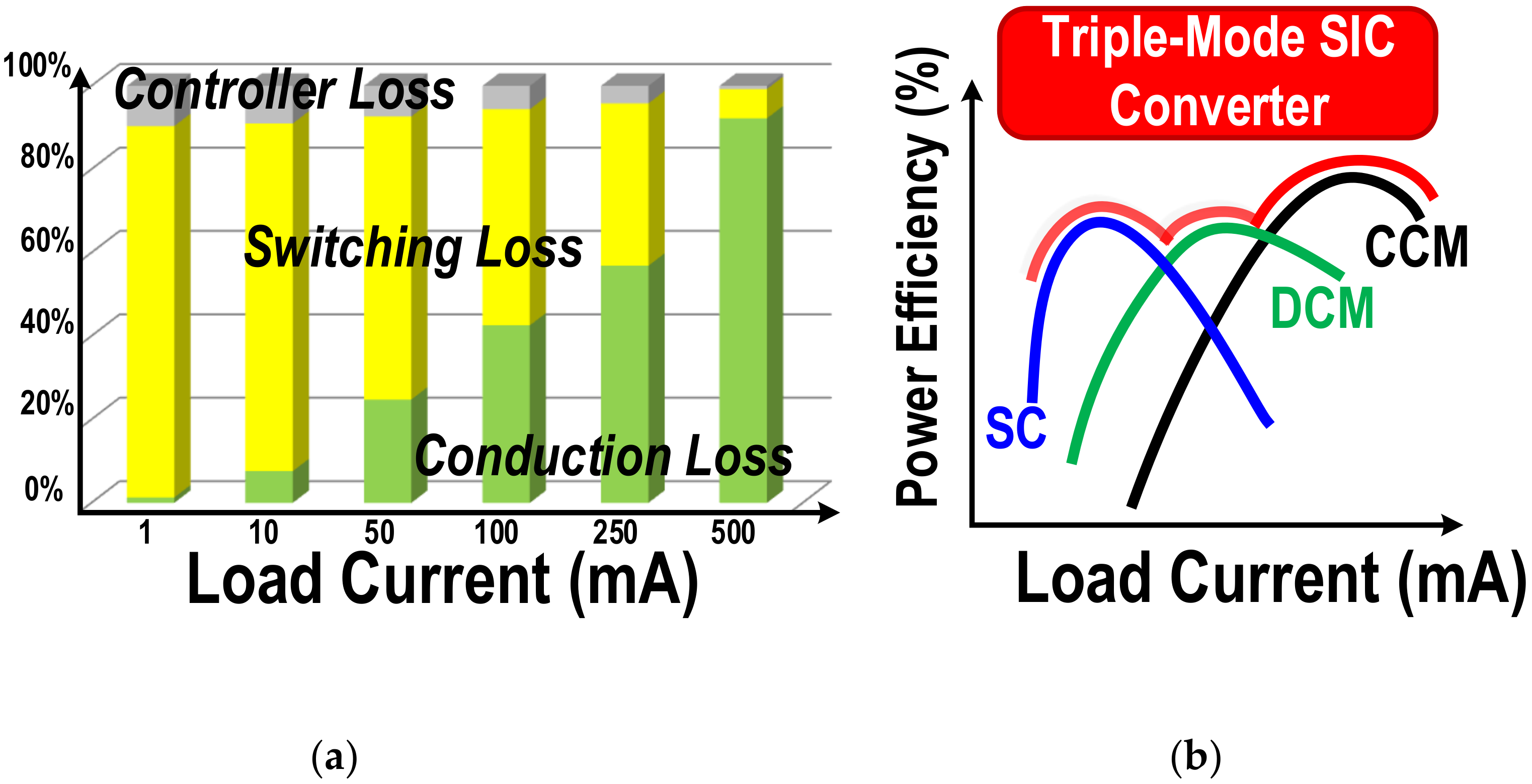
Figure 1a shows the proportion of different types of power losses across the load current range when the power stage with a constant input source is implemented on-chip and the operating switching frequency is fixed—conduction loss, switching loss, and controller loss—in switching type dc-dc converters among PMICs, such as a switched-inductor (SI) converter and a switched-capacitor (SC) converter. It shows that the ratio of the total power losses is strongly dependent on the load current level. Therefore, a suitable control method for minimizing power losses in different load conditions is required. As shown in
Figure 1b, an SI converter involving continuous conduction mode (CCM) control shows high efficiency in heavy load current conditions since conduction loss is dominant [
1,
2,
3,
4]. However, as the load current decreases, a reverse current flowing through the inductor is generated. The SI converter should then operate in the discontinuous conduction mode (DCM) rather than the CCM. Additionally, when variable frequency modulation (VFM) is used, the SI converter with DCM operation can reduce the switching loss to achieve high efficiency for light load current conditions [
1,
2,
5,
6,
7]. For the maximum efficiency of the SI converter operating in the DCM, a high-precision zero-current detector (ZCD) is necessary to prevent reverse current through the inductor.
Despite the SI converter operating in the DCM, it has a performance limit in ultralight load current conditions [
7]. The SC converter, which is another type of PMICs, uses only capacitors as energy transfer media, and no inductor is involved. Owing to its low controller and switching losses, it exhibits better efficiency than the SI converter in ultralight load current conditions [
8,
9,
10,
11,
12]. Even if the SC converter is also designed efficiently under heavy load conditions, a large number of large capacitors must be mounted on the outside of the chip, which can take up more PCB size than the SI converter with a single inductor. In addition, because of a predefined conversion gain, the efficiency of the SC converter can be significantly decreased as the input voltage changes. Accordingly, if a single converter can be designed to operate as an SI and an SC converter adaptively, high power efficiency can be achieved over the wide load current range for IoT devices, extending the battery usage time.
This paper, which is an expanded version of [
13], presents a triple-mode switched inductor-capacitor dc-dc buck converter that offers the advantages of both aforementioned converters.
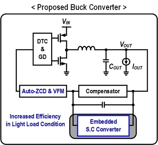
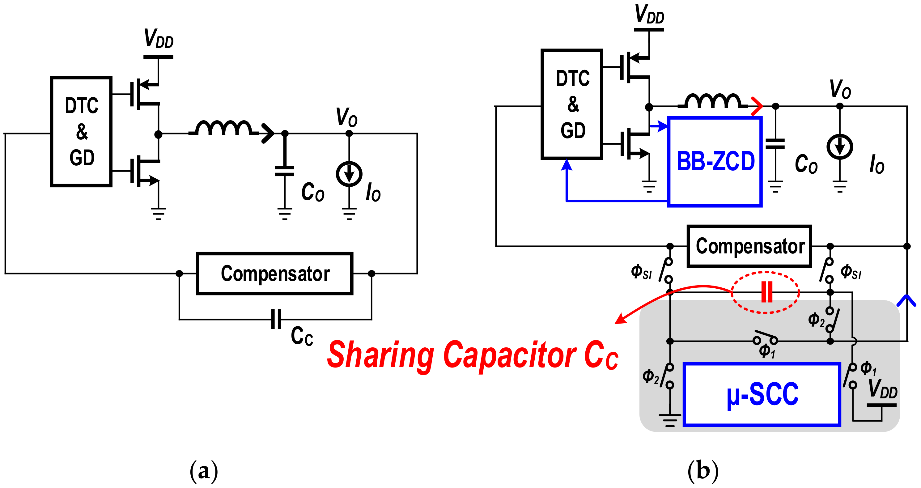
Figure 2a shows the conventional SI converter with a proportional-integral-derivative (PID) compensator requiring a large compensation-capacitor (
CC) for pulse width modulation (PWM). As shown in
Figure 2b, the proposed switched inductor-capacitor (SIC) converter reuses the Cc as a flying capacitor of the SC converter for the ultra-light load condition. Furthermore, a high-precision bang-bang ZCD is proposed for enhancing the power conversion efficiency when the SI converter operates in the DCM.
The rest of this paper is organized as follows.
Section 2 describes the overall architecture of the triple-mode SIC dc-dc buck converter.
Section 3 proposes a bang-bang zero current detector (BB-ZCD) that operates in the DCM.
Section 4 presents measurements and performance comparisons and
Section 5 provides the conclusions in brief.
2. Tripe-Mode Structure
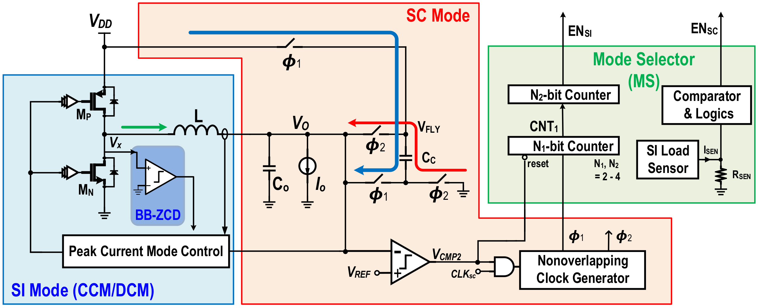
Figure 3 shows the overall structure of the proposed SIC dc-dc buck converter. As described above, since the ratio of the total power losses in the converter depends on the load current level, the proposed converter changes operating modes according to the load current (
IO). A mode selector (MS) manages and changes the operating mode as shown in
Table 1. When the SIC converter operates as an SI converter along with the main power switches
MP and
MN, and an inductor (
L) in either the CCM or the DCM, conventional peak current mode control is adopted. As a heavy load current is defined as a load current exceeding 20 mA, the converter can reduce dominant conduction losses in this heavy load current conditions if it is allowed to operate in the CCM with a fixed switching frequency. For a load current range from 2 to 20 mA, which corresponds to light load current conditions, VFM is applied in the DCM to reduce switching losses. Moreover, the BB-ZCD is proposed to enhance the power conversion efficiency at light load condition. In ultralight load conditions, corresponding to a current less than 2 mA, the power switches
MN and
MP and the PWM block used in the SI converter are turned off for the micro switched-capacitor converter (μ-SCC) mode with operation phases
Φ1 and
Φ2 without using the inductor. In this case, the large compensator capacitor
CC adopted for the stability of PWM in the SI converter is reused as a flying capacitor. For a given
CC and switching frequency, ultralight load current rage is determined as the higher efficient region than that of DCM operation. Therefore, owing to the capacitor sharing concept, even if two converter topologies are used as SI and SC converters, there is no additional size requirement for capacitors. Furthermore, as shown in
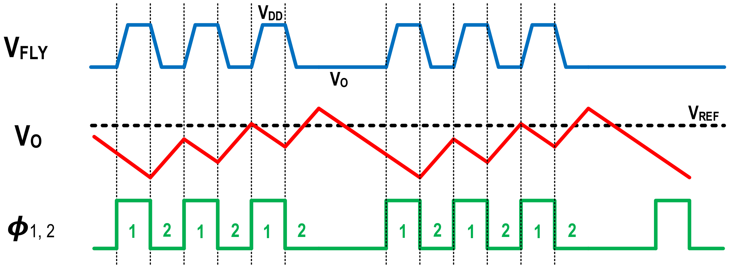
Figure 4, the converter in μ-SCC mode transfers the power to the output only when the output voltage (
VO) is lower than the reference voltage (
VREF). Then, the controller loss can be reduced because the feedback control loop can use only a hysteresis comparator without any complex control circuitry. Therefore, the proposed triple-mode SIC converter, which operates in the CCM, DCM, and μ-SCC mode, can achieve high efficiency over the entire load current range by changing the operating mode according to the load current conditions.
For automatic selection of the operation mode, the converter should sense the load current. The MS determines the operation mode as shown in
Figure 3. When the converter operates as an SI converter, the load current can be sensed and the mode can be easily switched to another mode owing to the use of an inductor-current-sensing network and the ZCD block in SI converter. However, when the converter operates as the μ-SCC mode, since most of the power hungry blocks are turned off, a load current sensor with low power consumption is required. To reduce the static power loss, the MS uses a digital counter for the load current sensor, which is newly proposed here.
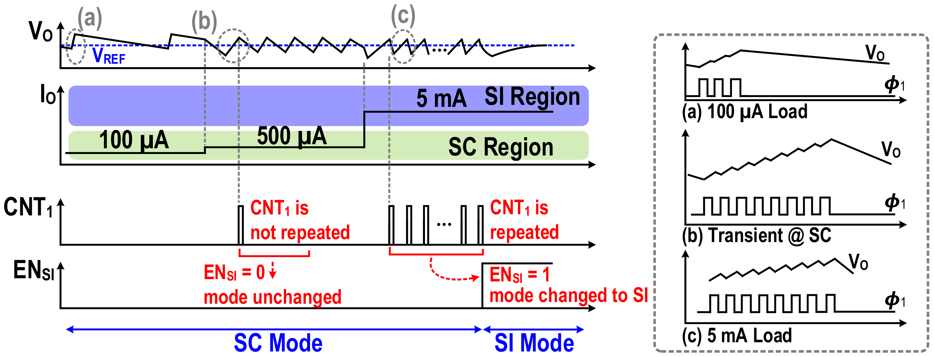
Figure 5 shows the output voltage
VO, load current
IO, output of the
N1-bit counter CNT
1, and an enable signal for the SI converter
ENSI as an example for a mode transition from the μ-SCC mode to the SI converter.
For the μ-SCC mode operation, the principle of charge conservation at both
Φ1 and
Φ2 should be satisfied:
where
VO1,
VO2, and
VDD are the output voltage at
Φ1 and
Φ2, and the supply voltage, respectively. The ripple voltage (
VO2 −
VO1) can be obtained from the relationship between the load current
IO and switching period
TSW as follows:
Substituting Equation (2) into Equation (3) gives
Since the sum of
VO1 and
VO2 is twice the average output voltage
VO in the steady state, we can write
This expression can be rewritten by including the switching frequency
fSW for the load current:
From Equation (6), it is evident that as the load increases, the switching frequency in the operation phases (Φ1 and Φ2) of the μ-SCC mode also increases. Therefore, counting the number of Φ1 pulses (N1) by using the N1-bit counter CNT1 can indicate whether the load current level reaches a certain threshold. Furthermore, an N2-bit counter is introduced to determine whether the mode change from the μ-SCC mode to the SI converter in DCM is required or not when a load current transition occurs. The ENSI becomes high only when CNT1 pulsates 2N2 times repeatedly. Such pulsation implies that the load current is high for a sufficiently long time, and it indicates that the mode should be changed to the SI converter. By contrast, for a small load current transition in the μ-SCC mode, since the CNT1 toggles only once or twice, resulting in maintaining ENSI in low level. Through this digital counter method, it can be determined whether a mode change from the μ-SCC mode to the SI converter in DCM should occur.
3. BB-ZCD for DCM
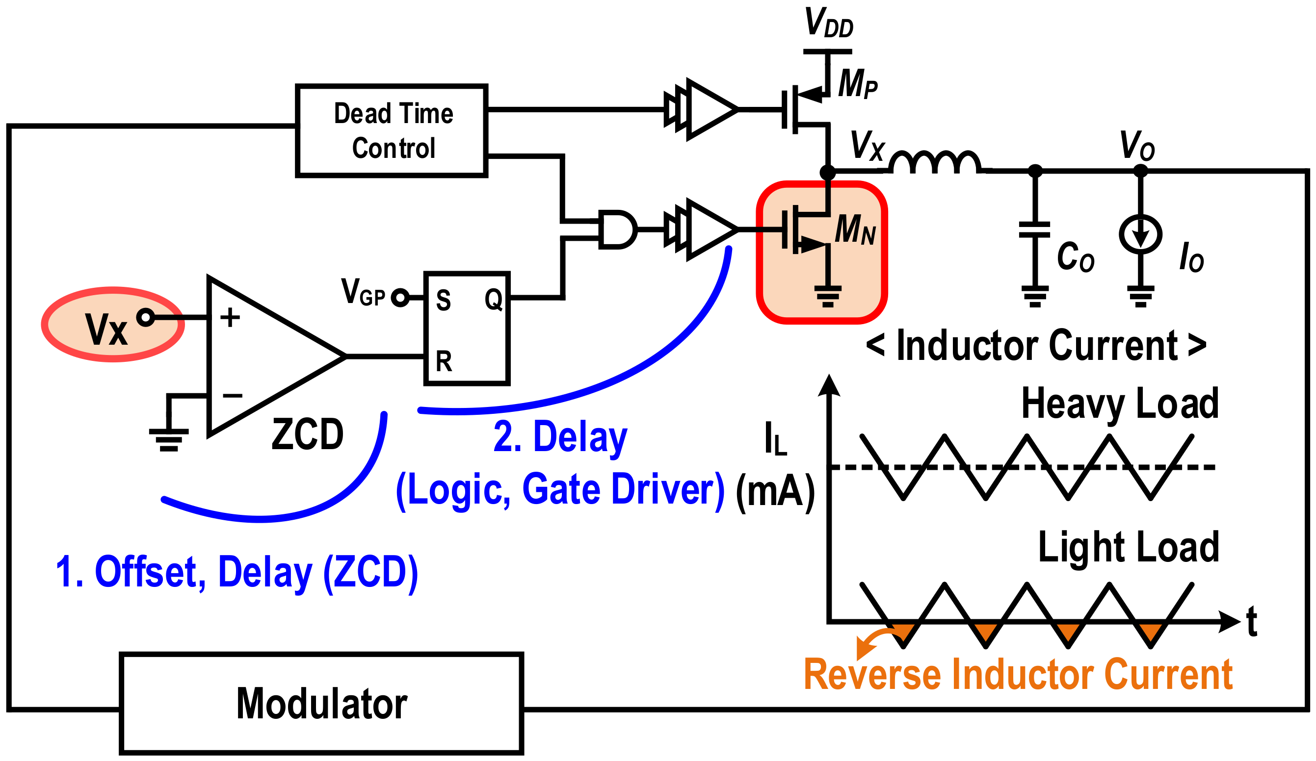
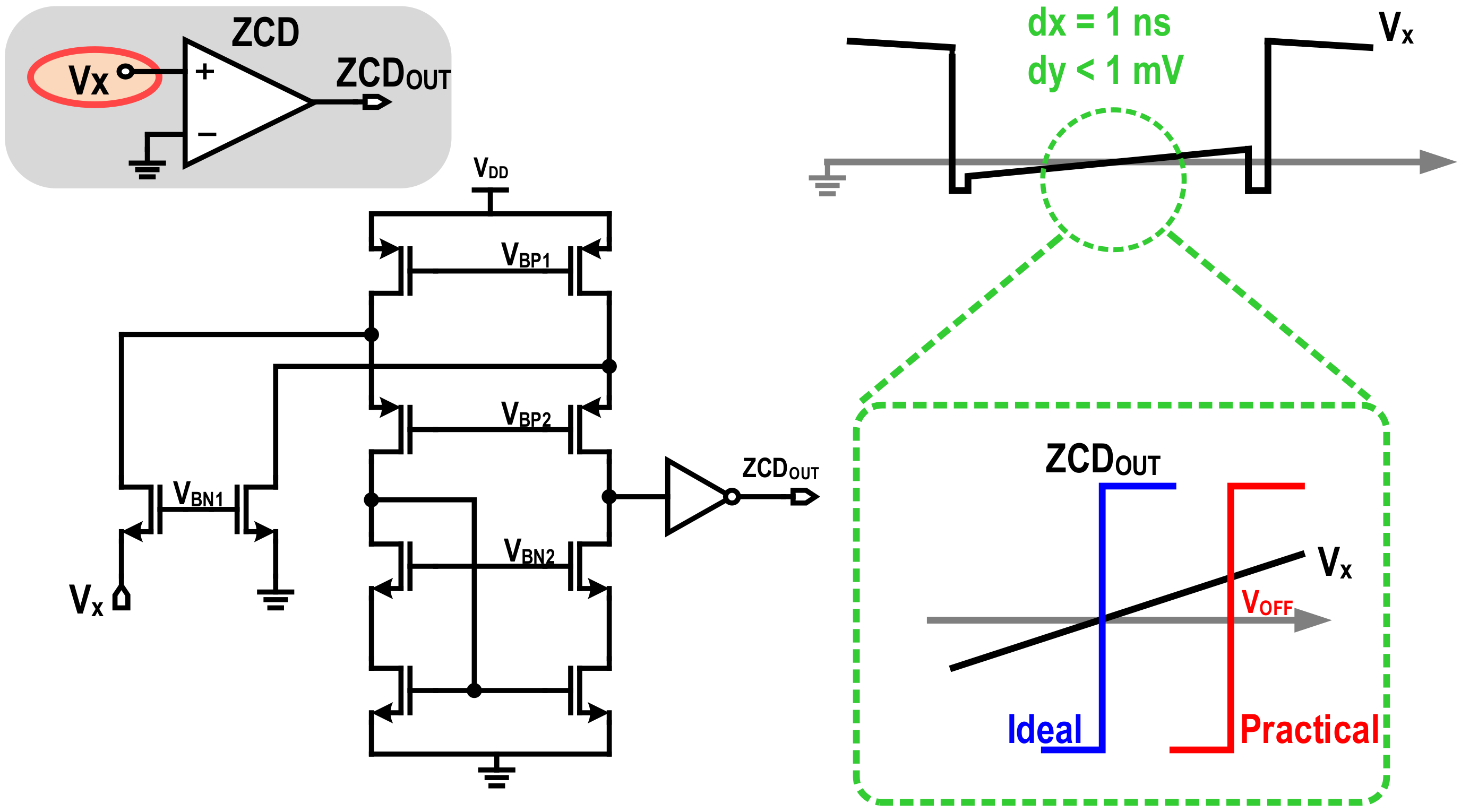
Figure 6 shows that when the load current in the SI converter decreases from a heavy load current to a light load current, it induces a reverse inductor current. For the prevention of this reverse current, the accurate ZCD is essential for the DCM. In general, the switching node
VX is monitored for the ZCD. This is because when a reverse current flows during the on time of the switch
MN, the polarity of
VX changes from a negative voltage to a positive voltage. Therefore, zero current detection is possible by comparing the ground voltage with the
VX voltage by using a comparator. However, as shown in
Figure 6, the conventional ZCD has the drawbacks of a delay, an offset, limited gain of the comparator, logic delay, and gate driver delay, rendering the ZCD incapable of determining the point where
VX is exactly zero.
Figure 7 shows a common-gate comparator is mainly adopted in the conventional ZCD to compare
VX with the ground voltage. However, if there is a delay and an offset in the comparator, it is difficult to realize a high-precision ZCD. This results in the flow of a reverse inductor current, which reduces the efficiency of the converter.
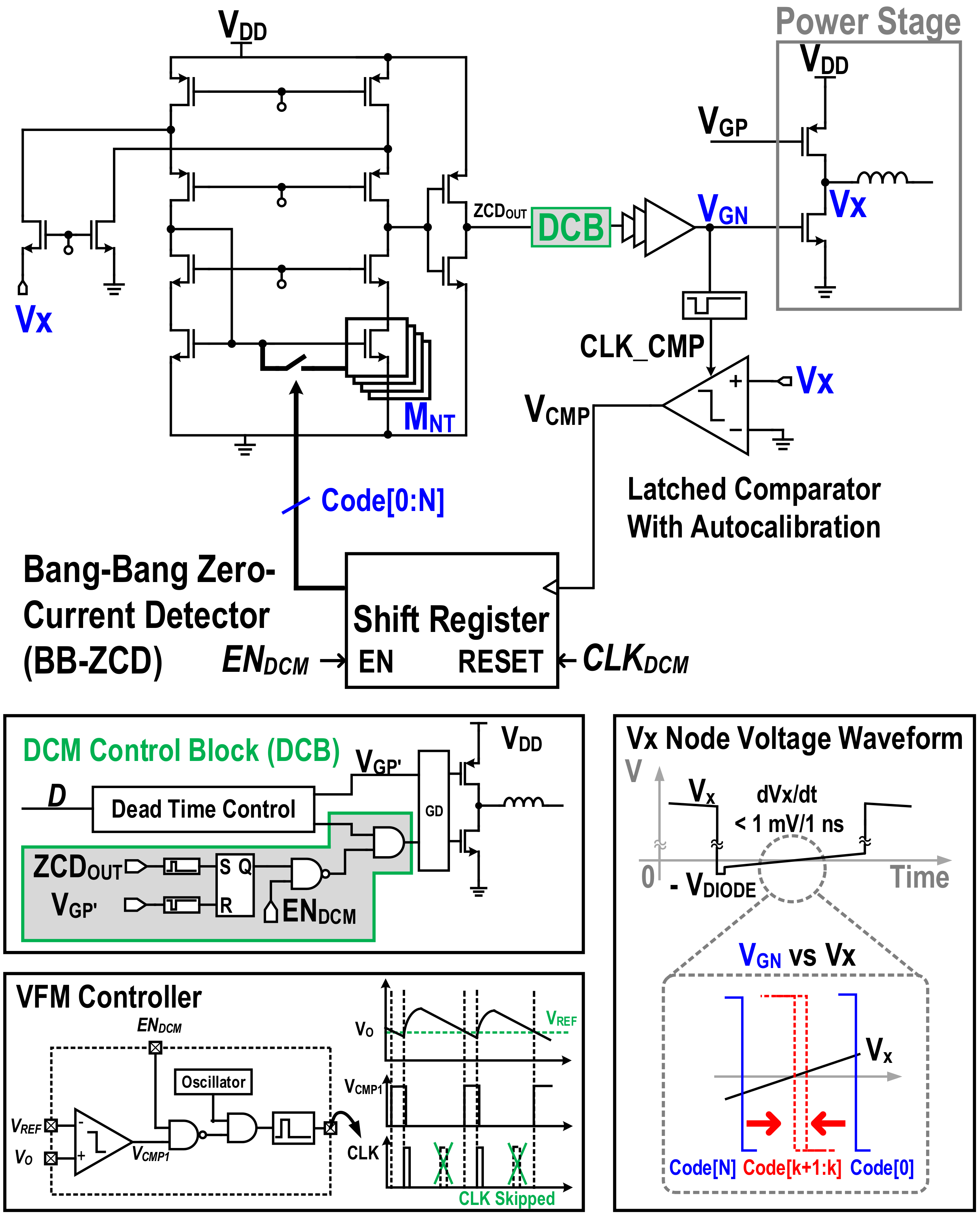
To solve the aforementioned problems, this paper proposes a BB-ZCD with a DCM controller involving autocalibration scheme through the gate signal (
VGN) of
MN, as shown in
Figure 8. The falling edge of
VGN is used as the clock signal of the latched comparator for digital feedback.
The latched comparator determines whether the polarity of the switching node VX is positive or negative when the VGN becomes low. If the falling edge of VGN is positioned after the actual zero-crossing point of VX, the output of the latched comparator becomes high, and the output code of the shift register increases. This up-counted output code increases the width of the sinking transistor (MNT) in the comparator, resulting in the falling edge of VGN occurring earlier in the next period. By contrast, if the falling edge of VGN is positioned before the actual zero-crossing point of VX, the output of the latched comparator becomes zero, and the output code of the shift register is down-counted. This reduces the width of MNT. Consequently, the VGN pulse becomes low at a later instant compared to the previous period. In other words, the latched comparator monitors whether the falling edge of VGN occurs before or after the actual zero-crossing time of VX and adjusts the sinking strength of the common gate comparator so that VGN converges to the optimal time while the shift register code converges to [k: k + 1]. Therefore, the digital feedback facilitates accurate zero current detection in the DCM.
However, a practical error factor in the latched comparator can cause a problem in the ZCD. If there is an offset in the latched comparator, the
VGN pulse eventually converges when
VX equals its offset voltage, not the ground level. Accordingly, the amount of offset acceptable in the latched comparator should be determined. Since the slope of
VX in our implementation is less than 1 mV/ns, if the offset exceeds 20 mV, similar to the offset in the conventional latched comparator, a considerable delay is introduced. For an allowable delay of 2 to 5 ns, the offset should be lower than several millivolts. Therefore, the latched comparator in
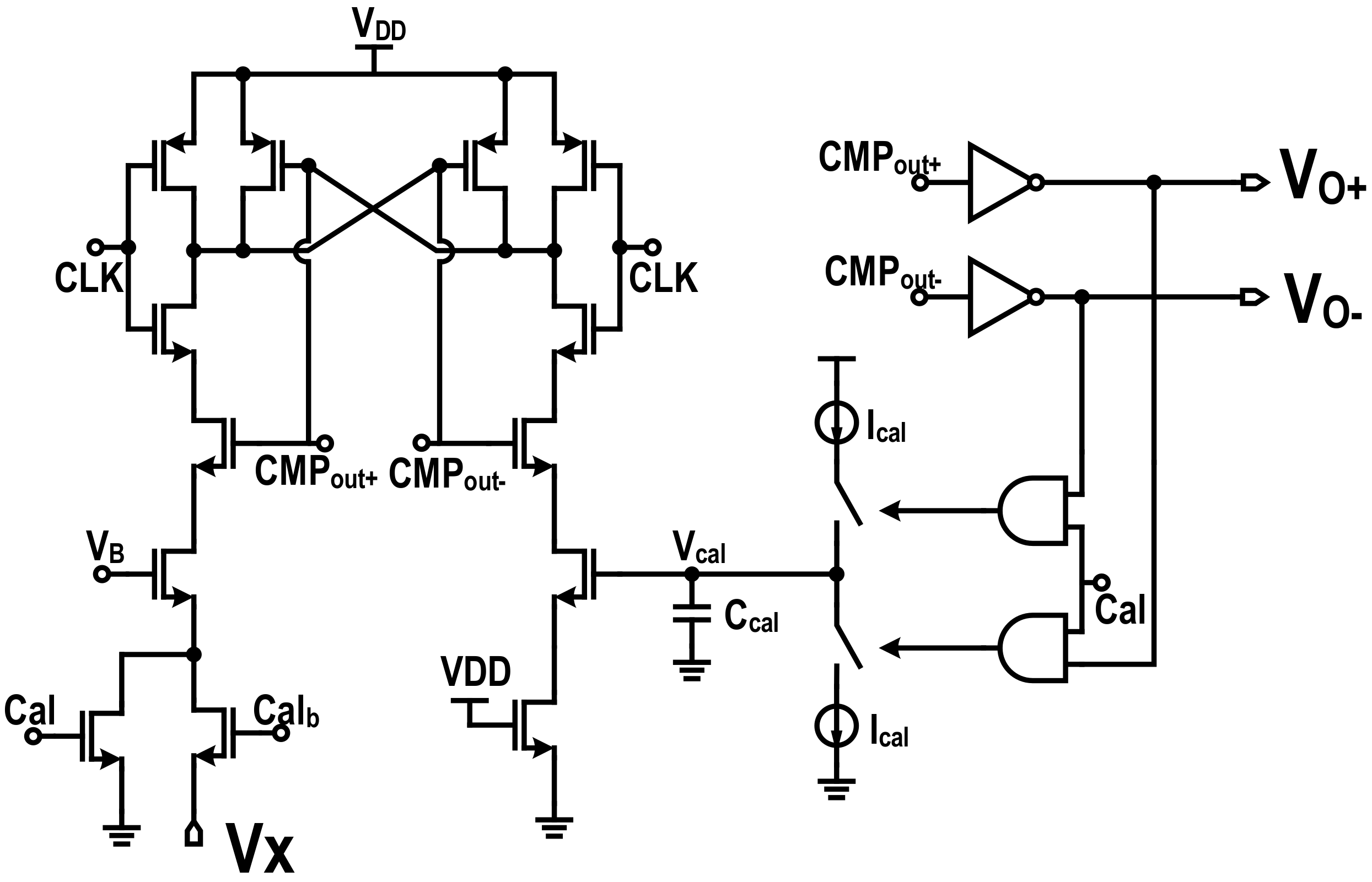
Figure 9 is adopted for ensuring a low offset [
14]. It has two operation phases, one for calibration (
Cal) and the other for comparison (
Calb). In the calibration phase, the two input nodes of the comparator are shorted to the ground, and the bias voltage (
Vcal) is adjusted to minimize its offset. If calibration is performed only once at the start-up time, the discharge of the calibration capacitor (
Ccal) at a later time would change
Vcal. Therefore, it is necessary to calibrate the offset periodically. For periodic calibration, the calibration phase is applied during the on time of the high side switch
MP because the BB-ZCD does not work during this phase. Thus, a high-precision BB-ZCD can be realized by using this low-offset latched comparator.
Figure 8 also shows the implementation of the clock skipping scheme to adjust the switching frequency for VFM control in the DCM. If there is no clock skipping, the output voltage
VO will saturate because of the unnecessary switching. Therefore, clock skipping is necessary to ignore the clock signal until
VO is less than
VREF. The VFM control involving this clock skipping not only prevents the divergence of
VO in the DCM but also reduces switching loss.
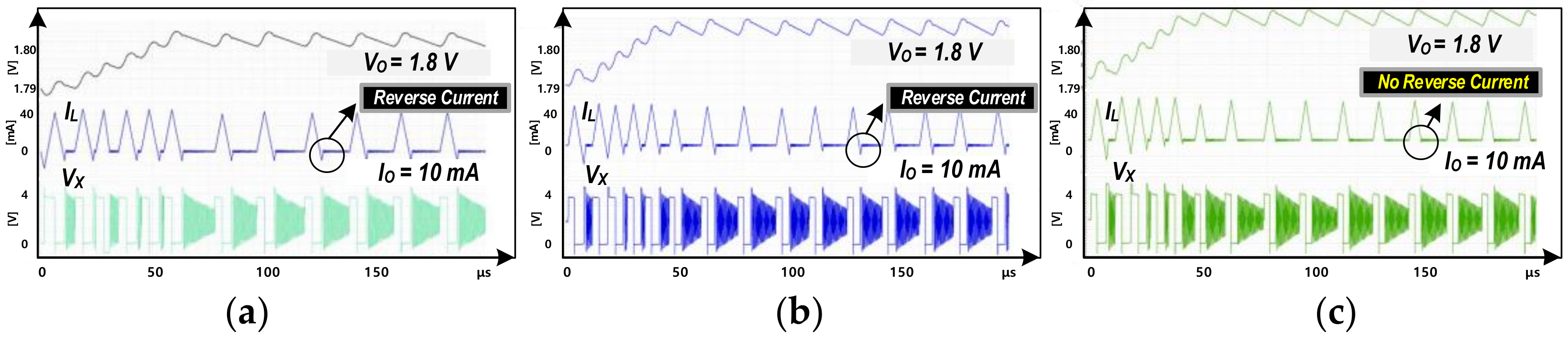
Figure 10 shows simulation results for
L = 4.7 μH,
CO = 4.7 μF,
VDD = 3.7 V,
VO = 1.8 V, and
IO = 10 mA.
Figure 10a corresponds to the case of the SI converter operating in the DCM and equipped with the conventional ZCD. Despite
VO being well regulated to 1.8 V, a reverse inductor current flows, resulting in low power conversion efficiency.
Figure 10b shows the simulation result for the SI converter in the DCM, using the proposed BB-ZCD. The offset of the latched comparator is 10 mV, and it is not calibrated. Although
VO is well regulated to 1.8 V, a reverse inductor current also occurs. This is because the code of the shift register converges to a point where
VX equals the offset of the latched comparator. In this simulation result, the output code of the shift register converged to code [2: 3].
Figure 10c shows the simulation result when the offset of the latched comparator is calibrated. The reverse inductor current gradually disappears since the inaccuracy of ZCD is progressively reduced. Finally, a regulated output and absence of a reverse inductor current are observed in the steady state. At this time, the output code converges to code [5: 6].
4. Measurement Results
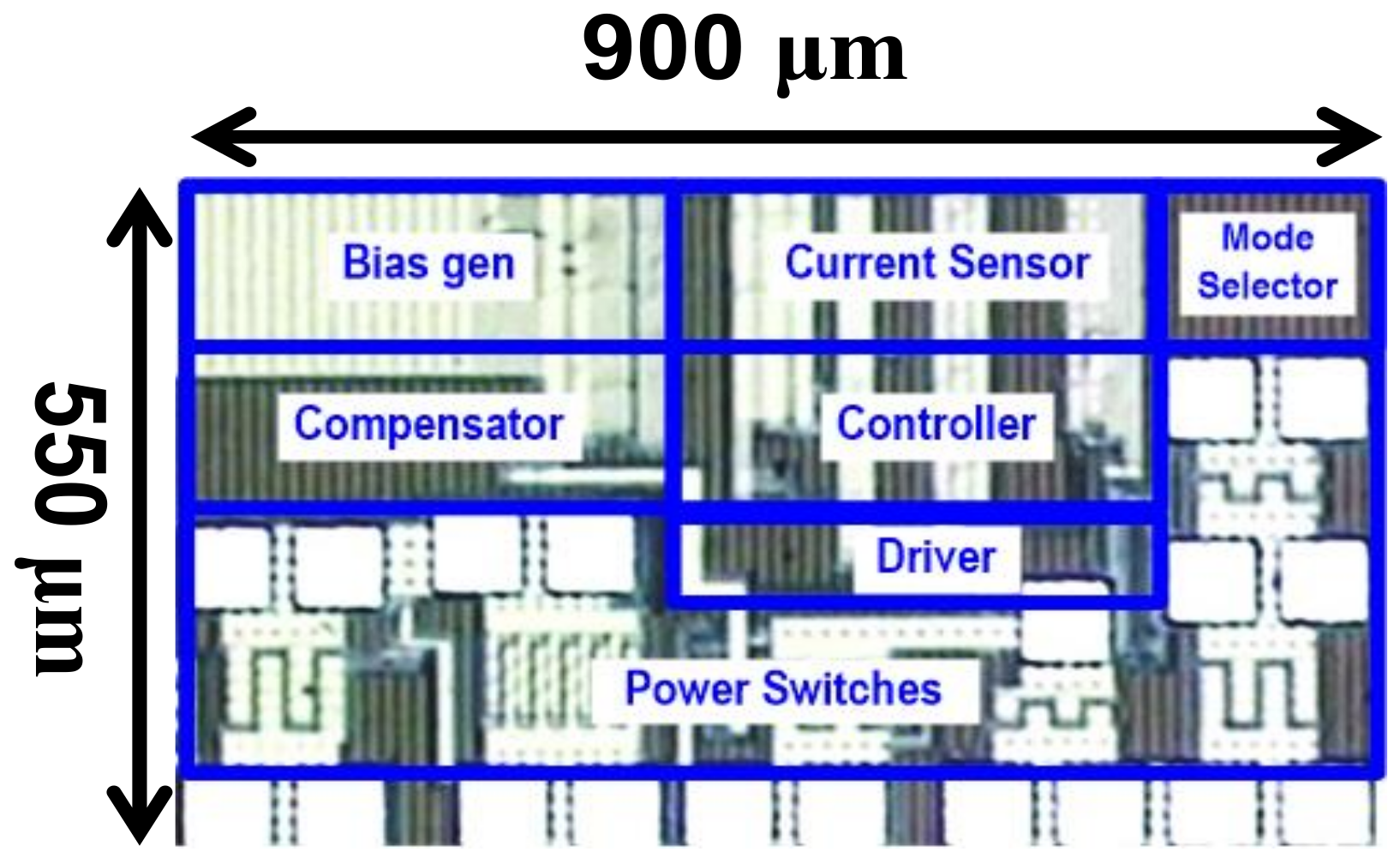
The proposed triple-mode SIC converter was fabricated in a 0.18 μm CMOS process, and the die area was 0.495 mm
2, as shown in
Figure 11. The supply voltage
VDD was 3.7 V, the output voltage
VO ranged from 1.2 to 1.8 V, and the load current ranged from 100 μA to 500 mA. The inductance and capacitance of the power filter were 4.7 μH and 4.7 μF, respectively.
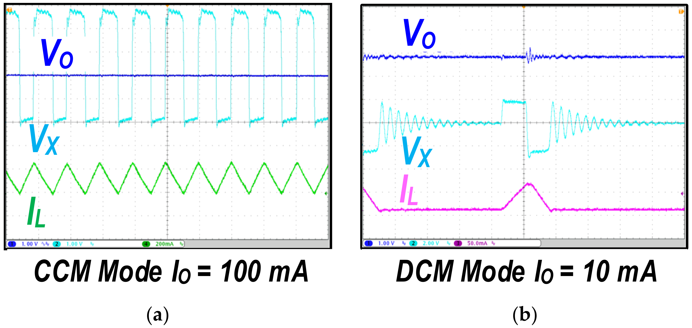
Figure 12a shows waveforms of the output voltage
VO, switching node voltage
VX, and inductor current
IL for a load current
IO of 100 mA and operation in the CCM with a fixed switching frequency of 1 MHz.
Figure 12b shows the measurement results for a 10 mA load current and DCM operation. The reverse inductor current is eliminated owing to the high-precision BB-ZCD.
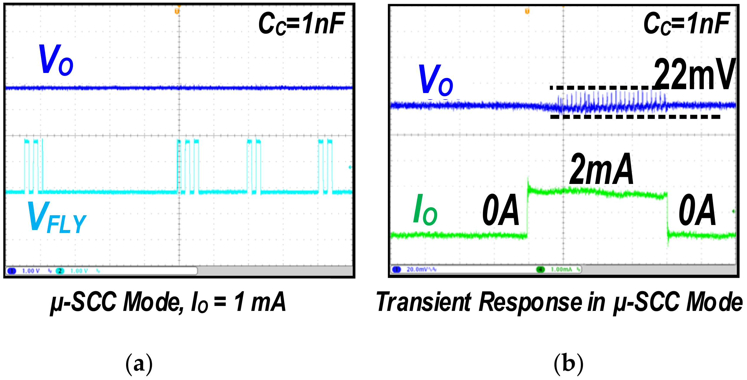
Figure 13a shows the waveforms of the
VO and top plate voltage of
CC (
VFLY) for a load current of 200 μA and operation in the μ-SCC mode when the
CC value of 1 nF is adopted in this paper. It can be seen that the proposed converter operates in the μ-SCC mode only when powering is required.
Figure 13b shows the load transient response in the μ-SCC mode when the load current varies between 0 and 2 mA. The MS can maintain the μ-SCC mode since the load current is still in the μ-SCC mode region.
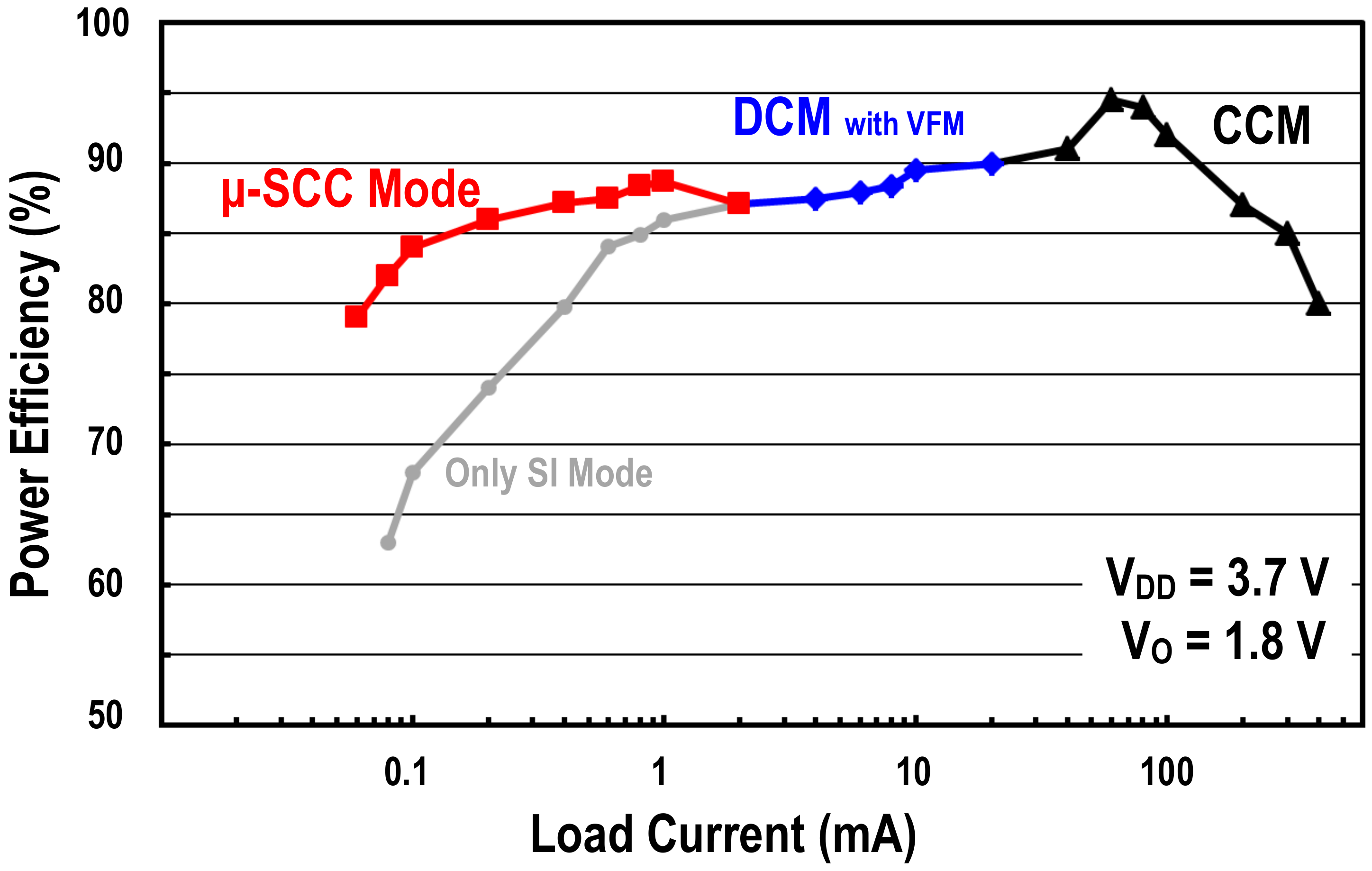
Figure 14 shows the power conversion efficiency plot of the triple-mode SIC dc-dc buck converter for the load current range from 60 µA to 400 mA, a 3.7 V supply, and an output voltage of 1.8 V. The maximum efficiency is 94.5% at the load current of 60 mA in the CCM. Furthermore, it delivers over 85% efficiency in the load current range from 100 µA to 300 mA.
Table 2 shows a comparison of the proposed converter with state-of-the-art dc-dc buck converters for light load conditions. The proposed converter shows higher efficiency than the other converters owing to mode transition among the CCM, DCM, and μ-SCC mode. In particular, the load current range for which the efficiency exceeds 85% is considerably wider in the proposed converter.


