1. Introduction
Nowadays, the use of renewable energies is a reality. According to recent articles of economic/business analysis and electric/electronic industry publications, in many countries, this type of energy represents a high percentage of the energy consumed. Nevertheless, international agreements against climate change suggest that the percentage of energy from renewable resources should increase in the coming years. Furthermore, it is necessary to increase the number of this type of facilities, and improve their efficiency [
1,
2]. A clear example is the imminent electrification and expansion of the transport sector that makes necessary direct links between renewable energy and electric vehicles (EVs), in grid power.
Within the renewable energies, photovoltaic (PV) energy is one of the most installed. To increase the installed power of this technology, it has been proposed to use more efficient technologies, and reduce the facilities’ cost [
3,
4]. Technological advances in solar power include the increased efficiency [
5], the reduction of overheads, reduced size of films, use of polymers, utilization of new materials for solar power cells, improvements of DC-AC converters for connection to the grid [
6,
7,
8,
9] and new architectures for power management.
There are several possible configurations for PV systems: (i) centralized configuration, where the PV panel can be connected together, and DC power is delivered to one converter; (ii) string configuration, when several PV panels are connected in rows, and each row has its own converter; and (iii) modular configuration, where each PV module is connected to one converter.
The most common PV plant topology consists of a specific module of PV panels connected in series, forming a string or array. The connection of several strings in parallel will configure the corresponding solar plant. There are several configurations for PV systems if we consider the DC bus connection [
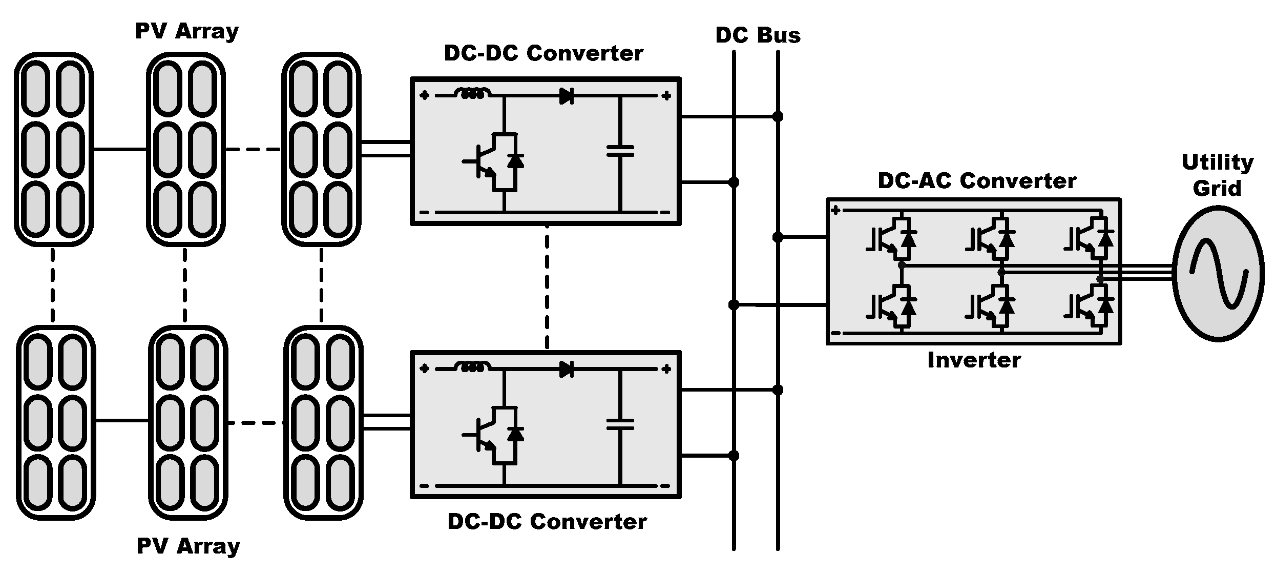
10]. A monopolar DC configuration uses a single wire; the return conductor may be land or metallic. Its main advantage is the use of a single cable. The PV plant is connected to a monopolar DC network through a DC-DC converter (
Figure 1). The converter will adapt the voltage level between the DC bus and the PV modules, so that maximum power is transferred to the system with the adequate control strategy. The energy injected to the DC bus can be transferred to the utility through a DC-AC converter. A different topology for the DC bus is the bipolar DC configuration [
11]. It consists of two wires, one with positive polarity and other with negative polarity. In normal operation, the current through ground is zero. It has two voltage levels, allowing, under fault conditions, a monopolar operation. The main advantage of the installation of a bipolar DC bus is the reduction in losses, which makes it possible to reduce the section of the wires, and therefore reduce the conductor volume or increase the transmission capacity. Finally, the DC bus can use a homopolar DC configuration. It has two or more wires with the same polarity, usually negative. The return may be by land or metallic. Its main advantage is the reduction in the costs of insulation; however, the return current is double.
This work proposes the use of a bipolar DC bus instead of the monopolar DC bus, for which a new DC-DC converter topology is proposed, which allows the connection of each photovoltaic string to this bus [
12,
13].
The connection of a distributed generation system with DC output to a bipolar network can be done in different ways. One of them is to include a DC-DC converter of one input and one bipolar output. When the appropriate control strategy is applied, this option allows setting the generator working point. Regarding the converters, different configurations have been proposed, both in isolated and non-isolated versions. Non-isolated versions are usually more advantageous than isolated versions, from the point of view of the efficiency, cost, volume and weight. The proposed DC-DC converter with one input and two outputs is based on the combination of two converters of one input and one output, such as the single-ended primary-inductor converter (SEPIC) and Ćuk [
14,
15,
16,
17]. It is a step-down/step-up converter. This topology is effective for this type of application, with high efficiency and with the use of only one controlled power switch. In addition, for the control of the maximum power point, any proposed technique for one input and one output converter can be used [
18,
19,
20,
21,
22,
23,
24].
The combined SEPIC-Ćuk converter has been theoretically analyzed in [
14,
15]. However, in this paper, a design procedure is established for the use of these converters in the connection of photovoltaic systems to bipolar DC networks. The operation of the converter is analyzed for a system isolated and connected to the network. On the other hand, a control strategy has been applied so that the photovoltaic system works at its maximum power point.
In this paper, a comparison between bipolar DC and monopolar DC grids is included in
Section 2. In
Section 3, the combined converter SEPIC-Ćuk topology is described. In
Section 4, an experimental prototype is designed, and a control strategy applied so that the set operates at the point of maximum power transfer. Experimental results are also presented. Finally,
Section 5 presents the conclusions of this work.
2. Monopolar Versus Bipolar DC Grid
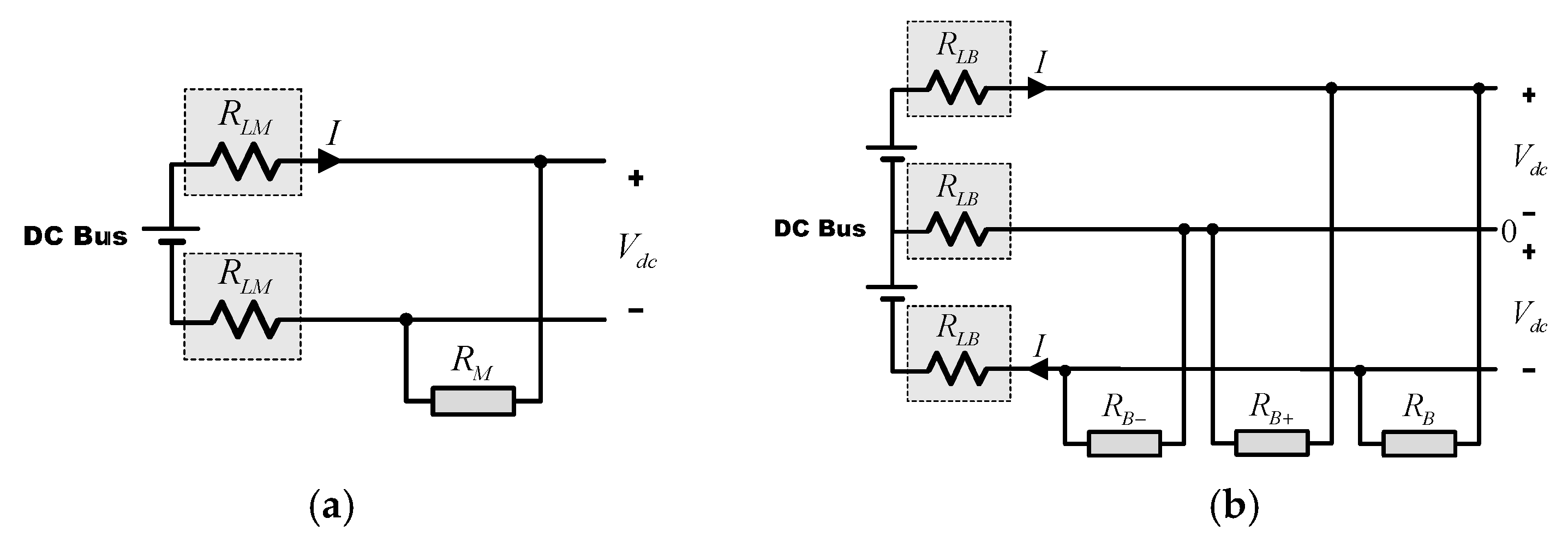
A monopolar DC grid consists of two wires between which a DC voltage is defined. Any load can be connected to this network at the voltage
Vdc (
Figure 2a).
On the other hand, the bipolar DC grid (
Figure 2b) is formed by three wires, “+”, “−” and “0”. Each load can be connected to two different voltage levels:
Vdc if the load is connected between “+” and “0” or between “0” and “−”, and 2
Vdc if the load is connected between “+” and “−”. Another characteristic to highlight is when the loads connected between “+” and “0” and between “−” and “0” are balanced, the current through the wire “0” is null; therefore, if this criterion is taken in consideration when the loads are connected, the section of this “0” wire can be significantly reduced.
In
Figure 2a,
RLM represents the resistance of the wires for a monopolar DC grid. In
Figure 2b,
RLB represents the wire resistances for the bipolar DC grid.
When the two topologies are compared, for the same power transmission conditions in both grids and wires of the same section, the power losses in the bipolar DC grid are a quarter of the losses that occur in the monopolar DC grid.
The comparison of the two topologies with the same losses and wires of the same section results that the bipolar DC grid can transmit twice as much power as in the monopolar DC grid.
Finally, when the power losses and the transmission power in both are equal, the relationship between line resistances in both topologies can be calculated. Therefore, the resistance of the bipolar DC grid is four times greater than the resistance of the monopolar DC grid. This means that the wire section in the bipolar grid is a quarter of the monopolar grid.
Therefore, from the point of view of the power losses, the transmission power and the section of the wires, bipolar DC grids have advantages with respect to monopolar DC grids, which are usually used.
3. Proposed Converter
The connection of a distributed generation system with DC output to a bipolar network can be done in different ways. One of them is to include a DC-DC converter of one input and one bipolar output. When the appropriate control strategy is applied, this option allows setting the generator working point. For the connection of a PV system to a bipolar grid, different solutions based on DC-DC converters have been analyzed [
8,
9]. Regarding the converters, different configurations have been proposed, both in isolated and non-isolated versions. Non-isolated versions are usually more advantageous than isolated versions, from the point of view of the efficiency, cost, volume and weight. In this sense, various configurations with bipolar output have been proposed in the literature, all of them have in common the use several power switches and several reactive components. In [
11,
25], a three-level boost converter was reported, to provide two bipolar output voltages. It required an inductor, two switches (one of them floating) and two diodes. In [
26], a three-level boost converter with two inductors was shown. It provided two bipolar output voltages also. Three-level boost converters are widely used in low-voltage bipolar-type DC microgrids. In the same way, a three-level DC-DC converter with coupled inductors for high-power applications was proposed in [
27]. A single-inductor power converter with buck–boost capability, two switches (one of them floating) and three diodes was presented in [
28], where the switches operated in overlapping mode. A bipolar output DC-DC converter was proposed in [
29], consisting of two basic DC-DC converters. The first one was a boost converter and the second was a DC-DC buck–boost converter. Both operated in a complementary way, in a series-combined boost and buck–boost converter. A dual-output DC-DC boost converter was reported in [
30], where it employed two inductors, two diodes and two switches.
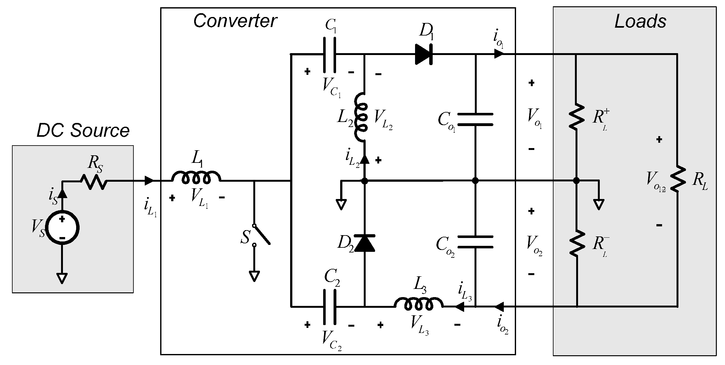
In this work, a converter based on the combination of SEPIC and Ćuk converters is proposed.
Figure 3 shows the configuration of this converter. This combination is based on the fact that both converters have the same input, one power switch and one input inductor. They have the same conversion ratio and the output of the Ćuk converter is inverted with respect to that of the SEPIC. Therefore, its combination allows obtaining a bipolar output voltage from a monopolar input.
This configuration employs only one power switch, three inductors, two link capacitors and two diodes. It has an advantage over the other proposals in that it has a reduced number of components. Only one power switch is necessary, which has its gate referenced to ground what simplifies the design of the gate drivers. This makes both the power switch and the input inductor concentrate all the input current, and it is also possible to couple several power switches and several inductors in parallel to distribute the current, allowing a synchronous or overlapping mode (the same control signal) or interleaved mode (shifting phase the control signals of each switch).
The converter can work in two operating modes: continuous conduction mode (CCM) and discontinuous conduction mode (DCM). CCM means that the inductor current is continuous. On the other hand, in DCM, the current of the inductor is discontinuous, i.e., in a time interval of the switching period, this current is zero.
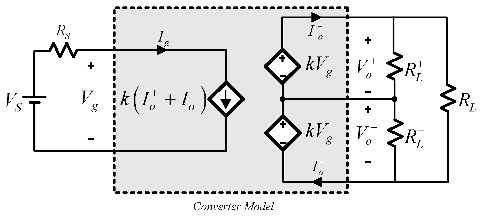
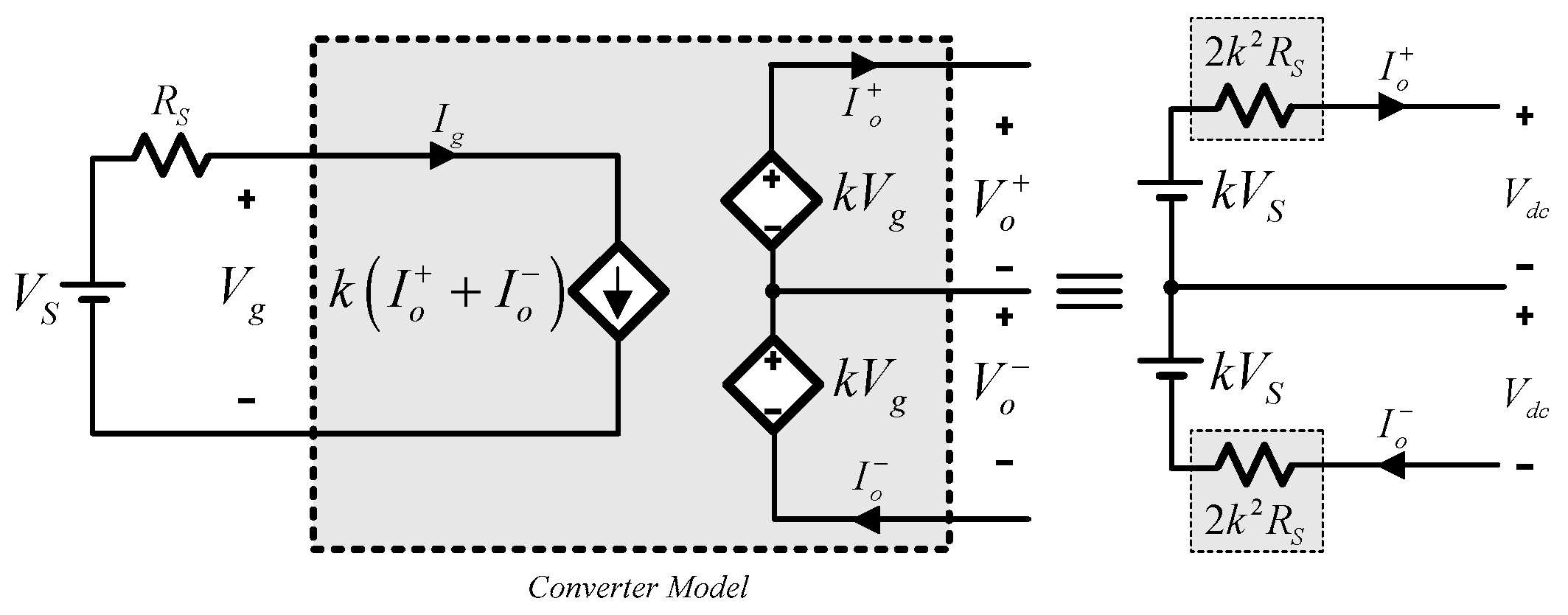
The operation of the converter, in steady state, can be analyzed through a simple model with controlled sources.
Figure 4 shows the equivalent circuit.
Rs and
Vs represent the equivalent of the DC source. The relationship between input and output variables can be expressed as
where the parameter
k depends on the operating mode of the converter. If the converter works in CCM,
k must be
where
D is the duty cycle.
In the case of DCM, the value of
k is given by the expression
Here,
TS is the switching period and according to
Figure 3,
Ro and
Leq are given by
In PV applications, the converter works by following the maximum power point of the source. For this, the following condition must be fulfilled:
Here, Rg is the equivalent resistance from the terminal of the controlled current source.
A PV system in isolated operation can be represented by the circuit shown in
Figure 4. At the input loop, the current is given by
That can be expressed in the way of
Therefore, according Equation (6), it must fulfill
Equation (9) is useful when the system is operating in isolated mode, since it allows to determine the duty cycle under different load conditions when the system is transferring the maximum power.
In many applications, the PV system is connected to a bipolar grid in parallel with other sources. When the same model of controlled sources is considered, the equivalent circuit from the bipolar network is useful because it allows the analysis of the power flows and establishing the range of powers when the converter works in CCM mode. In this case, from the terminals of the bipolar grid, the equivalent circuit of the converter can be obtained.
Figure 5 shows the equivalent voltage, which is
kVS, and the value equivalent resistance, 2
k2RS.
Under the conditions of maximum power
where
Vg is the output voltage of the PV system when the maximum power
P is transferred.
For a balanced bipolar grid of voltage ±
Vdc, at the positive output, transferred power can be expressed by
So, from the equivalent circuit in
Figure 5, the next equation can be established as
When
Io+ is substituted in Equation (12) from Equation (11)
Obtaining
k from Equation (13) and taking into account that the system must supply power, it is deduced
Therefore, k only depends on the voltage at the connection point of the converter and the output voltage of the photovoltaic system at the maximum power point (MPP).
Equation (14) allows to obtain the duty cycle of the converter for different conditions of grid voltage and input voltage at the MPP.
From the point of view of the converter component design,
Table 1 shows the average values of voltages and currents for each of the converter elements when it works in steady state. It is assumed that the converter operates in CCM. This mode of operation is the preferred in power systems due to its higher efficiency, so this operation mode is the most adequate for the proposed application. It should be noted that the voltage at the
C2 capacitor (Ćuk side) is higher than the voltage at the
C1 capacitor (SEPIC side). Choosing the appropriate values for the inductors and capacitors is of special importance for the proper operation of the converter.
The selection of the
L1 inductor depends on the desired ripple value of the input current. Its peak-to-peak value is given by
ΔiL1 is a percentage of the input current average.
For the choice of the
L2 and
L3 inductors, it is assumed that the converter works in CCM in a power range.
On the other hand, the combination of SEPIC and Ćuk converters works in CCM when the next expressions are fulfilled as
where
Leq and
Ro are defined according Equation (5).
The selection of the link capacitors C1 and C2, for the SEPIC and Ćuk sides, is based on assuming that the voltage in those capacitors must be constant. The resonant frequencies (ωr) must be lower than the switching frequency (ωS), in order to ensure constant voltage.
To ensure that the converter operation mode is neither discontinuous quasi-resonant mode (DQRM) nor discontinuous capacitor voltage mode (DCVM), the resonant frequency must be
In the same way, the voltage ripple in
C1 and
C2 is given by
The selection of the output capacitors
Co1 and
Co2 is also made to obtain the desired voltage ripple value. Its peak-to-peak value is given by
4. Experimental Prototype
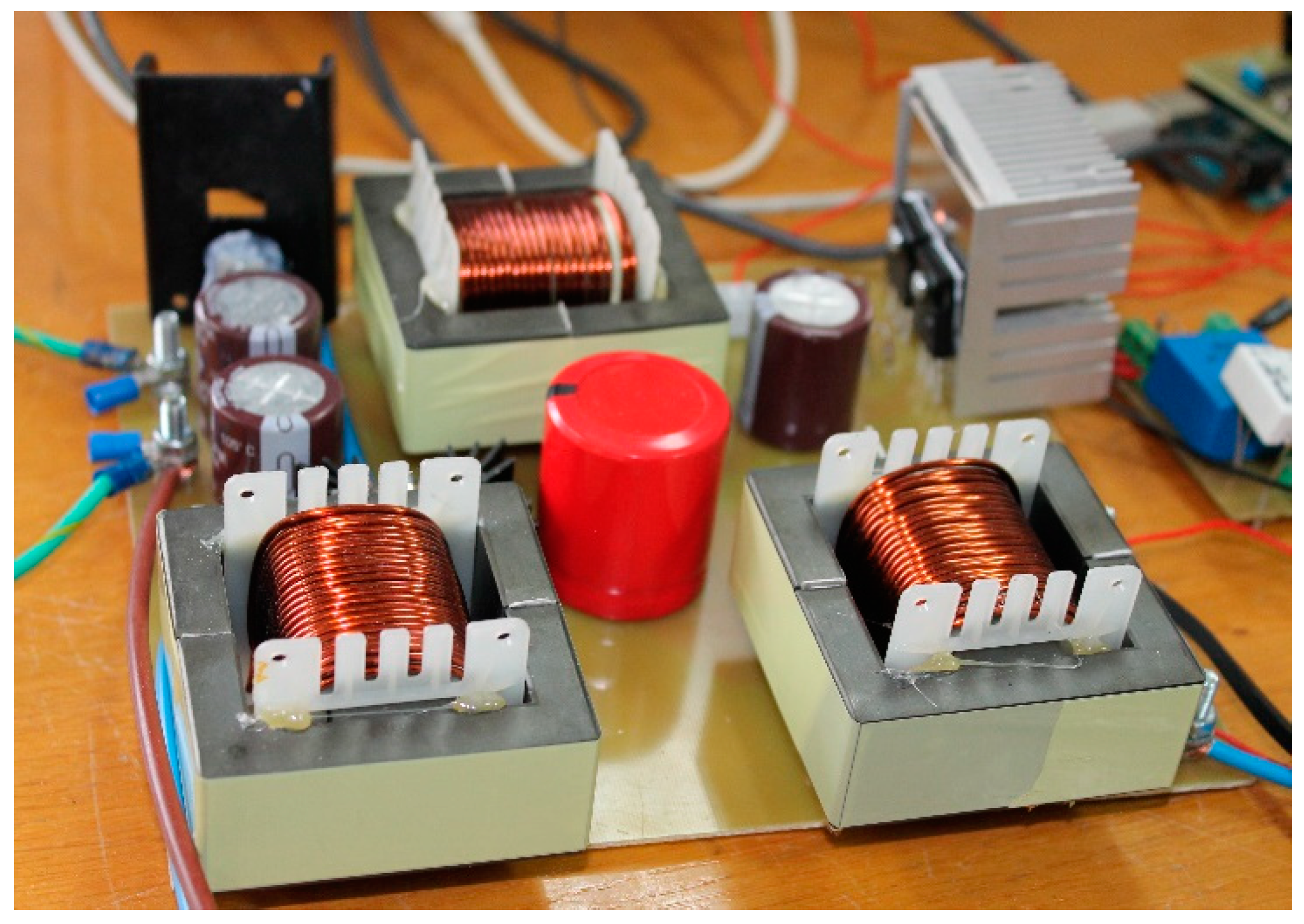
An experimental prototype of the proposed DC-DC converter has been designed, based on the circuit shown in
Figure 3. The prototype is a scaled model that allows the verification of its operation in the laboratory.
Figure 6 shows the experimental prototype.
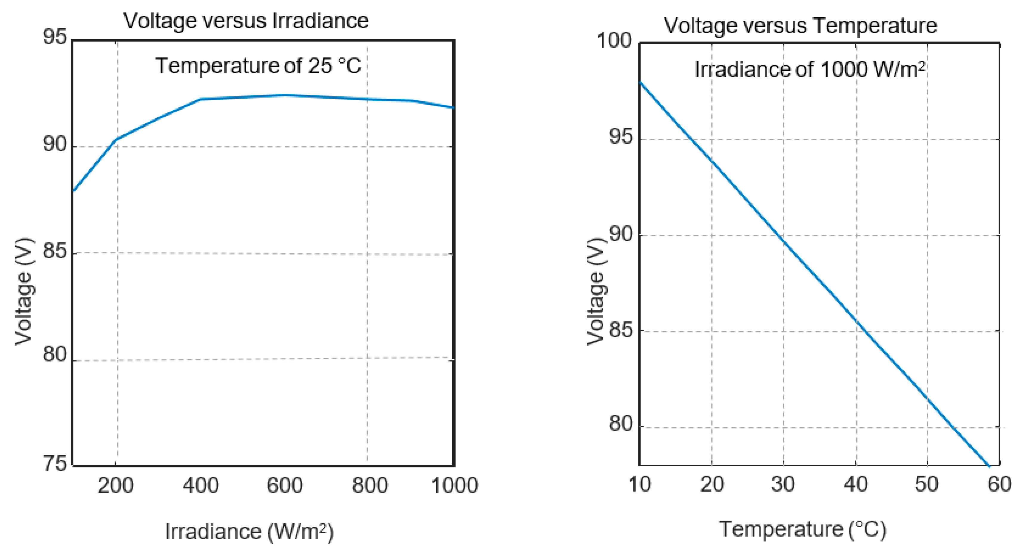
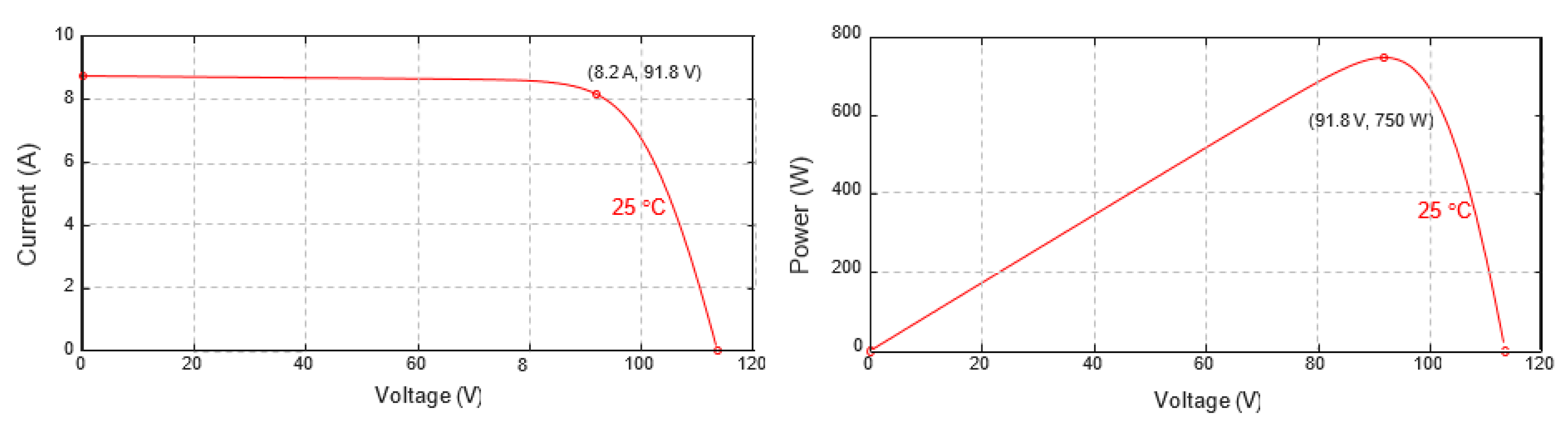
The designed converter allows the connection of a PV system to a bipolar DC microgrid of ±100 V. In this design, an array consisting of three monocrystalline photovoltaic modules from Isofoton, model ISF-250, have been considered.
Table 2 shows its performance at an irradiance of 1000 W/m
2 and cell temperature of 25 °C.
For this string, the open circuit voltage is 114 V and short-circuit current is 8.75 A.
In the maximum power conditions, the voltage varies from 85 to 92.5 V, depending on the irradiance, for a temperature of 25 °C. On the other hand, when the irradiance is 1000 W/m
2, the voltage varies from 75 to 98 V, according to the temperature.
Figure 7 shows the variation in the output voltage for different irradiances and different temperatures.
With respect to the power, it varies from 72 (100 W/m2, 25 °C) to 796 W (1000 W/m2, 10 °C), which will be taken as design values to the converter.
4.1. Converter Design
The selection of the components of the SEPIC-Ćuk combined converter shown in
Figure 3 is stablished according the peak power of the string where the converter will be connected. Therefore, the prototype will be designed for a power of 1 kW (0.25 kW above maximal power). The voltage at maximum power for different irradiance can vary from 75 to 98 V. Thus, according to Equation (14), the duty cycle of the converter will be between 0.51 and 0.57. The switching period is established at 40 µs.
Table 3 shows the main design features of the converter.
The maximum input current is given for the maximum power, it is 8.17 A. On the other hand, the maximum ripple of the input current is set to 4%. The application of Equation (15) results in an inductance, L1, of 5 mH.
For the lower power, 72 W, the input voltage is 88 V (100 W/m2, 25°C), and the maximum load Ro can be calculated, which results in Ro = 103 Ω.
If Ro+ = Ro− = Ro = 103 Ω, according to Equation (17), the inductance Leq must be greater than 0.47 mH. Furthermore, considering L2 = L3, its values will be of 1.03 mH. In this design, L2 = L3 = 1 mH was chosen.
For a switching period (Ts) of 40 μs and fS = 100fr, the Equation (18) are satisfied for a minimum capacity value of 101 μF (for C1 and C2). Therefore, a standard value of 470 μF is chosen. With respect to the voltage ripple, the application of Equation (19) with C1 = C2 = 470 μF allows to obtain a ripple of 0.4%, when the load is maximum, which is when D = 0.52 and Ro = 11.1 Ω.
Finally, for the selection of the output capacitors Co1 and Co2, Equation (20) is applied. For a low-voltage ripple, C = 470 μF has been considered, which provides an estimated voltage ripple of 0.4% for Vo+ and 0.1% for Vo−.
Table 4 summarizes the characteristics of the SEPIC-Ćuk combined converter components implemented.
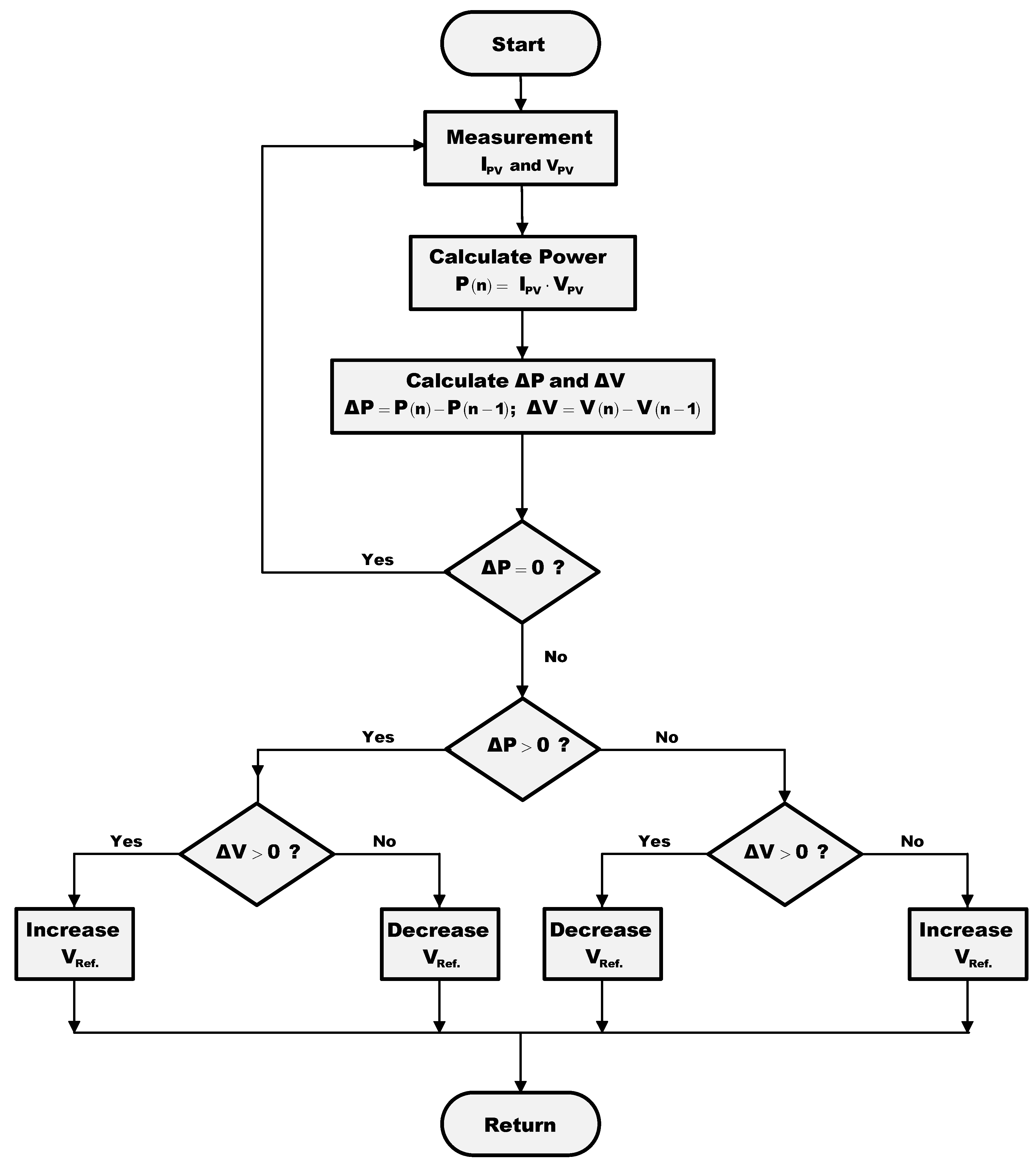
4.2. Control Strategy
For the control of the converter, several strategies can be applied to the proposals in the technical literature for converters of one input and one output [
18,
19,
20,
21,
22,
23,
24]. In this work, the technique chosen allows maximum power point tracking. The perturb and observe method (P and O) is one of the most used in practice [
24]. It is an iterative method where the reference voltage varies according to the increase in power, obtained from the input voltage and current to the converter.
Figure 8 shows the flowchart of the P and O strategy.
The control strategy has been implemented in the TMS320F28335 Delfino Microcontroller by Texas Instruments Dallas, Texas, USA. The measuring sensors used are the LA 25-NP for the currents and the LV 25-1000 for the voltage, both by LEM International SA, Geneva, Switzerland.
4.3. Experimental Results
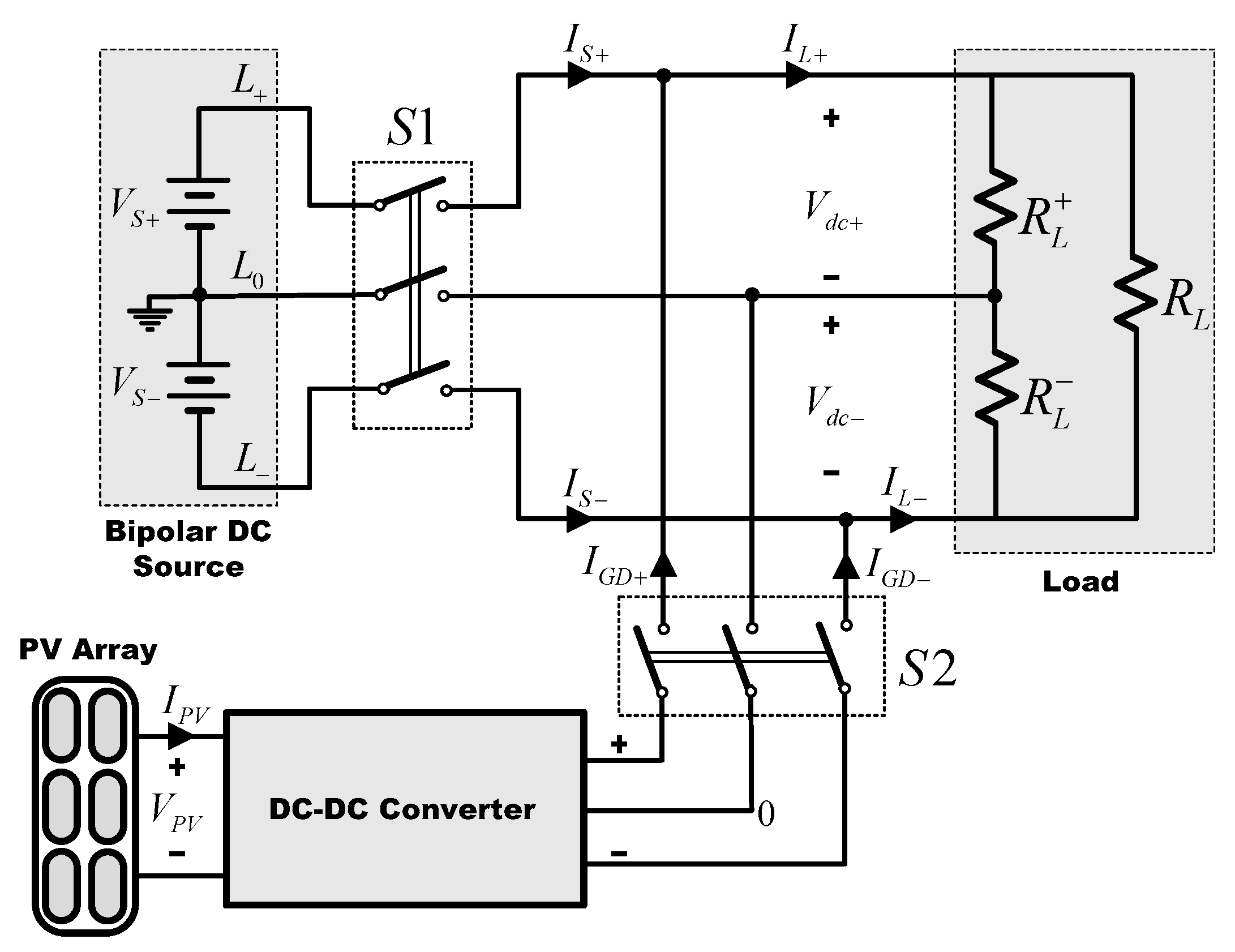
The experimental system set-up is shown in
Figure 9. The DC-DC converter will connect to a bipolar DC microgrid of ± 100 V. It has been designed for a maximum power of 5 kW. In the test, three resistors have been connected. They have the following values:
RL+ =
RL− = 47/2 Ω and
RL = 47 Ω.
When the switch S1 is closed and S2 is open, the Vdc+ and Vdc− voltages have an average value of 100 V. The current for each conductor is IL+ = 8.5 A and IL− = − 8.5 A, so that the power consumed by the set is 1.7 kW.
The PV system is emulated by a DC source, so the point of maximum power can be adjusted to a desired value, modifying its internal resistance and voltage.
Figure 10 shows the curves
I-
V and
P-
V of a photovoltaic string of three series of modules of Isofoton ISF-250 for a given irradiance. In this situation, the maximum power is given for 750 W with a voltage of 91.8 V and a current of 8.2 A.
The DC source is adjusted to an output voltage of 182.4 V, with an internal resistance (Rs) of 11.1 Ω. Therefore, the DC source will transfer the maximum power (750 W) when it supplies a current of 8.17 A and with an output voltage of 91.8 V.
In the following test, the switch
S1 is open and the switch
S2 is closed. Thus, the PV system is operating in island mode. According with Equation (4),
Ro = 5.9 Ω for the resistance values
RL+,
RL− and
RL. Therefore, the application of Equation (9) let the obtaining of
k = 0.73, resulting in a theoretical duty cycle of 42%. The measured power is 638 W, the voltage
Vdc+ =
−Vdc− = 62.5 V and the currents
IL+ =
−IL− = 5.1 A. With respect to the current (
IPV) and voltage (
VPV) at the input converter, their average values are 8.2 A and 92.1 V, respectively. Thus, the efficiency is 84.4%.
Figure 11 shows the gate source signal,
Vg, drain source voltage,
Vds, and the input current waveform. The measured duty cycle in these conditions is 41%, similar to the theoretical value.
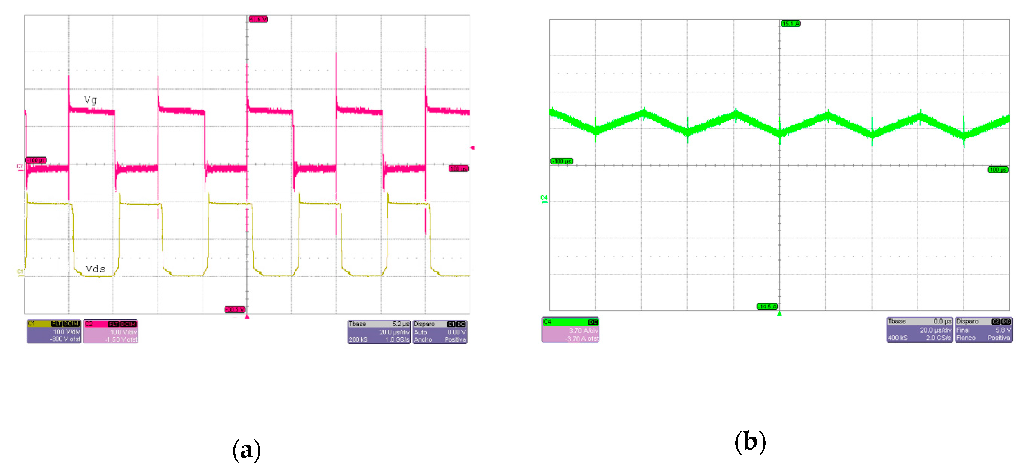
When the PV system and source are connected (
Figure 9,
S1 and
S2 are closed), the voltages at the point of connection are
Vdc+ =
−Vdc− = 99.7 V. From the theoretical point of view, Equation (14) must be fulfilled, therefore at the maximum power point,
k must be 1.09 and the theoretical duty cycle will be 52%. The converter supplies a current
IGD+ = −IGD− = 3.2 A, so the power transferred by the converter is 638 W. The input voltage (
VPV) is 92 V and the input current is (
IPV) 8.1 A.
Figure 12 shows the gate source signal,
Vg, drain source voltage,
Vds, and the input current waveform. In this case, the measured duty cycle is about 51%. In this test, the measured efficiency of the converter is 86.5%.
5. Conclusions
Bipolar DC grids have become an adequate solution for high-power DC microgrids. When compared with monopolar DC grids, their main advantage lies in a greater power transmission capacity.
A distributed generation system can be connected to the bipolar DC microgrid through DC-DC converters. There are different converter configurations with bipolar output, however, all of them have several power switches. In this paper, a converter based on the combination of a SEPIC and a Ćuk converter is proposed. This topology has, as main advantages, a reduced number of components and the use of a single switch.
In the proposed converter control strategy, any of the techniques described in the literature applied to converters of a single output can be used. Among the different control strategies applied to PV systems, the most commonly used are those that allow maximum power point tracking.
In this paper, an experimental prototype DC-DC converter with bipolar output based on the combination of SEPIC and Ćuk converters was developed. This converter allows the connection of a PV system to a bipolar DC grid. In the control, the perturb and observe method has been applied which has allowed maximum power point tracking. The results obtained allowed to verify the behavior of the converter with the applied strategy.


