Abstract
Recent advances in semiconductor technology provide us with the resources to explore alternative methods for fabricating transistors with the goal of further reducing their sizes to increase transistor density and enhance performance. Conventional transistors use semiconductor junctions; they are formed by doping atoms on the silicon substrate that makes p-type and n-type regions. Decreasing the size of such transistors means that the junctions will get closer, which becomes very challenging when the size is reduced to the lower end of the nanometer scale due to the requirement of extremely high gradients in doping concentration. One of the most promising solutions to overcome this issue is realizing junctionless transistors. The first junctionless device was fabricated in 2010 and, since then, many other transistors of this kind (such as FinFET, Gate-All-Around, Thin Film) have been proposed and investigated. All of these semiconductor devices are characterized by junctionless structures, but they differ from each other when considering the influence of technological parameters on their performance. The aim of this review paper is to provide a simple but complete analysis of junctionless transistors, which have been proposed in the last decade. In this work, junctionless transistors are classified based on their geometrical structures, analytical model, and electrical characteristics. Finally, we used figure of merits, such as , , and , to highlight the advantages and disadvantages of each junctionless transistor category.
Keywords:
junctionless; transistor; nanowire; double gate; planar; gate-all-around; FinFET; thin film; tunnel 1. Introduction
The concept of junctionless transistor (JLT) was introduced by J. E. Lilienfeld in the 1920s [1]. The main feature of this device is the absence of any pn junction; hence, the requirement of doping concentration gradients is avoided. It simplifies the fabrication process of the transistors with sizes below 10 nm. There are two main requirements to realize JLTs. First, the transistor channel must be highly doped (∼1 × cm). Second, the channel thickness has to be in the nanometer scale (∼10 nm). Due to the limitations in the microfabrication technology, it took more than 80 years to realize the first junctionless transistor. The first successfully fabricated JLT was a junctionless nanowire (NW), which was realized at the Tyndall Institute by Colinge et al. [2]. This device turned out to be the first one of a new generation of transistors. In the last decades, many other junctionless devices were proposed, which includes FinFET [3,4,5,6,7,8,9,10,11,12,13,14,15,16,17,18,19,20,21,22,23], Gate-All-Around (GAA) [24,25,26,27,28,29,30,31,32,33,34,35,36,37], Single Gate (SGJLT) [38,39,40,41,42,43,44,45,46,47,48,49,50], Double Gate (DGJLT) [51,52,53,54,55,56,57,58,59,60,61,62,63,64,65,66,67,68,69,70,71,72,73,74,75], Thin Film (TFT) [76,77,78,79,80,81,82,83,84,85,86], and Tunnel FET (TFET) [87,88,89,90,91,92,93,94,95,96,97]. Because most of the review papers on JLTs were published in 2010–2014 [98,99,100,101,102], a complete overview on the basis of the latest developments is missing. Therefore, in this paper, we provide a critical analysis of JLTs in terms of structure and performance comparison.
2. Classification
Junctionless transistors can be divided in two main categories: depletion-based and tunnel-based JLTs. In depletion-based devices, the amount of electrical current flowing through the device depends on the dimension of the depletion region, which is controlled by the applied gate voltage. In tunnel-based devices, the electrical current is governed by band-to-band tunneling (BTBT). JLT categories can be then classified based on the geometrical shape, material composition of the channel, as well as the gate structure. When a single gate on the top of the channel controls the current through the device, it is known as Single Gate junctionless transistor. If an additional gate is present below the channel, then it is called Double Gate junctionless transistor. If the transistor channel thickness is very thin (≤10 nm) and the channel material is not monocrystalline silicon, then it is known as Thin Film junctionless transistor. Gate-All-Around JLTs are characterized by a gate electrode that entirely surrounds the channel of the transistor; the channel can be either cylindrical or rectangular. When the transistor channel is a tube-shaped nanostructure, it is called junctionless Nanowire. If the electronic device is a fin-shaped transistor, it is called junctionless FinFET. This simple classification is coherent with the analyzed literature, whose distribution is shown in Figure 1. Although most of the reported junctionless transistors are inorganic electronic devices, organic solutions were also proposed [103,104,105,106,107,108]. In this work, we focus on inorganic junctionless transistors, where the following parameters as considered as the main figures of merit: the Drain-Induced Barrier Lowering (DIBL), which represents the drain voltage influence on the threshold voltage, defined as [109]; the Subthreshold Swing (SS), which can be defined as the change in the gate voltage required to decrease the drain current by one decade () [110]; the ratio, which is the ratio between the maximum available drain current, (, ), and the current in the off state, (, ).
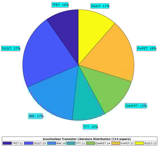
Figure 1.
Junctionless transistor literature distribution analyzed in this work.
3. Analysis
3.1. The First Junctionless Transistor
In 2010, J. P. Colinge et al., fabricated the first junctionless transistor (Figure 2) in the form of a nanowire characterized by a silicon thickness of 10 nm and a channel length of 1 m [2]. The process requires uniform and heavy doping (≥1 × cm) of the nanowire in order to ensure the correct operation of the device [111]. The nanowire transistor was realized over a SOI (Silicon on Insulator) wafer and patterned by electron-beam lithography.
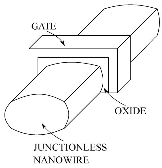
Figure 2.
Structure of the junctionless nanowire.
Junctionless NWs do not work in inversion mode (IM) like conventional MOSFETs. The threshold voltage is defined as the gate voltage that fully depletes ( state) the device layer (Figure 3c) [112,113]. Thus, the state definition is more similar to that of accumulation mode (AM) devices (Figure 3b); also from an analytical point of view, they can be modelled from AM device descriptions, since the current flowing in the device can be decomposed into two components: a bulk and an accumulation current [114,115]. When the gate voltage is greater (in absolute value) than the threshold voltage, partial depletion takes place creating a path in the substrate for the bulk current. When the gate voltage reaches the flat band voltage, the whole channel becomes conductive ( state), and an accumulation current starts to form at the semiconductor/insulator interface [112].
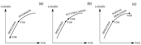
Figure 3.
Current behavior in (a) inversion mode (IM), (b) accumulation mode (AM), and (c) junctionless transistors.
The threshold and flat band voltages are of critical importance, since they determine the operating range of the device [2]. The threshold voltage can be extracted as the gate voltage at which the curve (where is the transconductance) drops to half of its maximum value [116]. It increases (in absolute value) with increasing doping, while decreasing with increasing gate oxide thickness, nanowire width, and length [117]. An analysis of the doping concentration influence on the threshold voltage is also reported in [118]: by increasing the doping concentration from 1 × cm to 1 × cm, the threshold voltage decreases from V to V; this could be attributed to the fact that, for high doping concentration, more carriers are available for the same gate voltage. An interesting characteristic of the flat band voltage is the dependency on the temperature. A detailed analysis of this parameter is presented in [119,120], in which it is shown that the flat band voltage decreases as the temperature increases. For low temperature ( K) and high doping concentration (1 × cm), the thermal energy is not strong enough to ionize all of the dopants. This results in an incomplete ionization that causes the series resistance to increases (Figure 4) and the drain current to decrease.
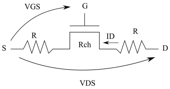
Figure 4.
Junctionless nanowire resistance model representation.
As reported in [121], junctionless nanowire transistors present a reduction of short channel effects as compared to inversion mode devices, but they are highly sensitive to the series resistance. The simulation of junctionless NWs with channel length of 100 nm and doping concentration of 1 × cm provided an intrinsic source/drain resistance of k. By decreasing the doping to 5 × cm, the resistance reached a value of 11 k. The performance of junctionless nanowire transistors can also be affected by current leakages that are associated to gate tunneling. The latter phenomenon is directly proportional to the length and width of the transistor (so to the gate surface area), and to the temperature [122,123].
Because the current in junctionless transistors flows far from the gate oxide/channel interface, the mobility degradation is minimized. This is one of the main advantages of depletion-based junctionless transistors with respect to the conventional ones [124]. Enhanced mobility in junctionless NWs was also attributed to the reduction of the scattered impurities that are caused by an overall smaller charge of ionized impurities [125]. Junctionless NWs were also investigated in terms of crystal orientations and material channel (germanium and silicon) and compared to inversion mode devices; the junctionless NW found to be less sensitive to short channel effects, presenting smaller , reduced , and higher than inversion mode transistors. As compared to silicon JLTs, germanium junctionless NWs were observed to be slightly more sensitive to short channel effects, but more competitive from an electrostatic control point of view [126,127,128].
3.2. Gate-All-Around
Figure 5 shows a schematic of a cylindrical junctionless Gate-All-Around transistor. The device, as the name suggests, is characterized by a channel entirely surrounded by the gate. The channel geometry determines the complexity of the equations that are needed to model the device behavior. In this case, the solutions to the Poisson equations are more complex, since cylindrical coordinates have to be introduced [26,31]. Additionally, GAAFETs with rectangular channels are reported, but they suffer from performance degradation due to corners effects [25]. An important parameter in the design of GAAFETs is the channel length. For a channel length reduction from 40 nm to 16 nm, the increases from 12 mV/V to 123 mV/V, while the increases from 62 mV/dec to 82 mV/dec [29]. The channel radius determines the device speed; lower radius corresponds to faster operation [26].
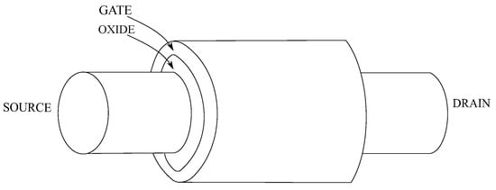
Figure 5.
Three-dimensional (3D) structure of a cylindrical junctionless GAAFET.
With respect to inversion mode devices, junctionless GAAFETs generally present higher ratio and less short channel effects [25,30]. Regarding the low-frequency noise (LFN) behavior, junctionless GAAFET is almost not sensitive to gate bias and doping concentration variations [28]. Instead, the intrinsic gain and cutoff frequency were observed to be degraded by the hot carrier effect; a relative degradation of for both of the analog parameters was reported [32]. The designer could improve the analog performance (small signal parameters and drain current drivability) by adding source and drain extensions, as shown in Figure 6 [24]. The structure that is depicted in Figure 5 can be further modified in order to increase the device performance. For example, a gate insulator made of hafnium oxide () instead of silicon oxide () can enhance the and the [27].
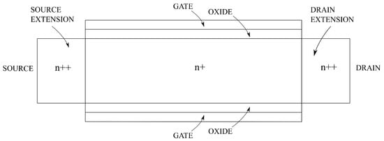
Figure 6.
Cross-sectional view of improved cylindrical GAAFET through addition of source and drain extensions.
Apart from engineering the gate oxide structures, the designer could also increase the number of gates. If two gates are present, the structure is defined as a twin gate transistor (Figure 7). Such a structure allows implementing logic gates easily since two inputs are present [34]. The twin gate structure can also be applied to a double channel GAAFET, as shown in Figure 7b. A fabricated twin gate double channel GAAFET showed an ratio of 7 × , a of 83 mV/V, and a of 105 mV/dec [33]. Besides silicon and polysilicon channel junctionless GAAFETs, devices composed of other materials were also reported: a gallium arsenide junctionless GAAFET was simulated, leading a value near to the theoretical limit ( mV/dec at K) [27]. A germanium junctionless GAAFETs was compared to a silicon one, and it provided lower , and ratio (data in Table 1) [35]. The channel material composition also influences the threshold voltage sensitivity to the temperature: considering silicon, gallium arsenide, indium arsenide, and indium phosphide, the minimum and maximum threshold voltage variations were observed for indium arsenide and silicon, respectively [37].
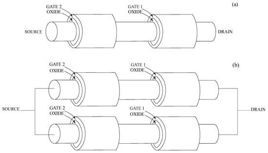
Figure 7.
3D Structure of (a) twin gate single channel GAAFET, (b) twin gate double channel GAAFET.

Table 1.
Reported figure of merits of junctionless GAAFETs. and are the channel length and width, respectively.
It is possible to use strain technology in order to further increase the device performance; a layer of SiN is deposited and, depending on the deposition conditions, the strain could be compressive or tensile [36]. The figures of merit of reported junctionless GAAFETs are presented in Table 1.
3.3. FinFET
Figure 8a shows a schematic of a bulk junctionless FinFET. The device can also be fabricated on the top of an insulator layer, as shown in Figure 8b. In that case we define it as an SOI FinFET. Dimensions of these transistors strongly affect their performance. Considering bulk junctionless FinFETs, increasing the fin width (W) from 6 nm to 15 nm can lead to a variation of approximately and for and , respectively; changing the gate length () from 12 nm to 21 nm can lead to a variation of approximately for and for [12]. Variations in the fin height (H) are more critical in terms of analog performance [19]. With respect to the inversion mode device, the junctionless FinFET presents lower . This is attributed to the low carrier concentration and high electric field in the middle of the channel in the state. As compared to SOI FinFETs, the bulk structure presents an additional degree of freedom in the design: by varying the doping concentration of the substrate from 1 × cm to 1 × cm, a change of in the threshold voltage can be obtained [4]. Furthermore, it also provides lower and . From an analytical point of view, it can be modeled from conventional triple gate (TG) structures [3,20]. An alternative structure is the so-called SON (Silicon On Nothing). In this structure, the silicon layer is isolated from the substrate through a selective etching. This design choice implies a more complex fabrication process with respect to the bulk structure [5].
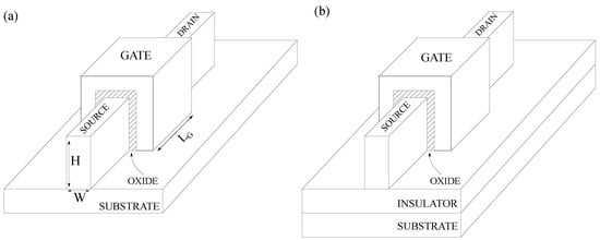
Figure 8.
3D FinFET structure: (a) bulk, (b) SOI.
The designer could follow different approaches in order to optimize junctionless FinFETs: work function engineering of the gate to reduce (by changing the gate work function from eV to eV, can be reduced by five order of magnitudes) [7]; spacer engineering to improve performance (e.g., dual-k spacers architecture can provide an improvement in by and in by ) [9]; doping engineering by using a Gaussian doped channel, which can lead to an increase in by [10,13], or a lightly doped channel, which allows for better gate control on the device [11]; gate oxide engineering to provide higher performance (in terms of and ) by the implementation of complex hetero gate oxide structures [8]. For example, the double hetero gate oxide (DHGO) presented in Figure 9 can obtain a higher with respect to conventional and triple/quadruple hetero gate oxide (THGO/QHGO) structures.
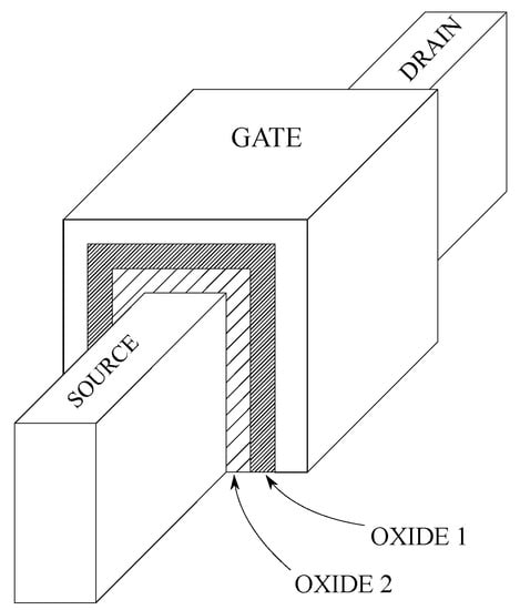
Figure 9.
3D double hetero gate oxide FinFET structure.
Besides the number of hetero gate oxides regions, it is also important to consider their dielectric constant value: for high values () the is reduced and the analog performance is degraded [14]. Instead, dual-k structures with intermediate values of the dielectric constant (, ) provide better performance with respect to those with low dielectric constant (, ) when considering random dopant fluctuation in the fin [16]. The latter is a critical phenomenon, especially for junctionless FinFETs, since they are more likely to be affected by random dopant variability [17]. Moreover, random dopant fluctuations and work function variability are considered to be more dominant with device dimension scaling [18]. It is important to note that the results reported for the junctionless FinFETs do not necessarily hold for the other junctionless transistors: for instance, the threshold voltage of junctionless FinFETs is more sensitive against work function variations as compared to that of junctionless GAAFETs [15].
FinFETs were analyzed by considering different materials for the device layer. A FinFET made of polycrystalline silicon is reported as a cost-effective solution with respect to silicon devices [22]. A GaAs FinFET with of 1 × compared to a silicon FinFET with an of 1 × was proposed. The better performance was attributed to the higher depletion of carriers when the device is in the state [21]. More complex structures were reported: InGaAs junctionless FinFET with alloyed Ni-InGaAs source and drain [23]. Table 2 presents the main figure of merits of the reported FinFETs.
Table 2.
Reported figure of merits of junctionless FinFETs. is the equivalent gate oxide thickness, while k is the gate oxide dielectric constant.
3.4. Single Gate
The single gate junctionless transistor presents two types of structures, i.e. bulk and SOI, as shown in Figure 10. The bulk structure provides more control on the device characteristics because of the possibility to dope and bias the bulk well [38]. When considering an n-type JLT with p-type bulk, it is possible to improve the hot carrier effect, thus reducing the current by positively biasing the well. On the other hand, by increasing the bulk bias, the threshold voltage can be decreased while increasing and . The degradation is even more relevant if the channel length is below 20 nm [40]. If the substrate doping concentration is high, then the current is minimized [44]. Moreover, it has to be considered that bulk junctionless transistors present reduced effective thickness, as compared to SOI; if a bulk SGJLT has a physical thickness of 10 nm, the effective thickness is 5 nm, because of the built-in junction potential [38]. With respect to the SOI structure, the bulk SGJLT presents improved analog performance: improved output transconductance, output resistance, Early voltage, and intrinsic gain [39]. When compared to junction transistors, the junctionless ones were observed to be more sensitive to the ratio, and to provide a lower . This is attributed to the highly doped channel, which increases the scattering effect, thus lowering the mobility [42].
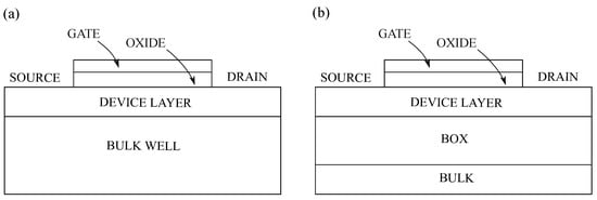
Figure 10.
Cross-sectional view of a single gate junctionless transistor: (a) bulk, (b) SOI.
More options are available to the designers in order to optimize the SGJLT; gate work function engineering can lead to an improvement of in the ratio [41], while a non-uniform (Gaussian) doping concentration through the device layer can reduce the [43].
As for FinFETs and GAAFETs, an improvement of the electrostatic characteristics of the transistor can be obtained by implementing high-k spacers, as shown in Figure 11a. The high-k spacers enhance the fringing electric fields; as a result the device is depleted not only below the gate but also laterally. This implies an increment of the effective channel length, which, in terms, improves the [45]. Designers can also enhance the transistor mobility and currents through S/D engineering and dual-k spacers structures [46,47].
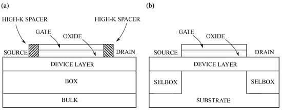
Figure 11.
Cross-sectional view of: (a) Single Gate junctionless transistor (SGJLT) with high-k spacers. (b) SGJLT with SELBOX.
A variant of the conventional SOI structure is the SELBOX (selective buried oxide), as shown in Figure 11b. This oxide configuration improves the transistor thermal isolation, allowing for an increment for the of 6 orders of magnitude (from × to × ) [48]. Moreover, the SELBOX architecture increases the gate control on the device, since a junction is formed between the highly doped channel and the substrate. The junction enhances the device layer depletion. Designers could also add a metal layer on the top of the BOX layer. This enables the formation of a Schottky junction that could help to fully deplete the transistor in the state [50]. Regarding leakages in junctionless transistors, one of the most critical cause is associated to the parasitic BJT (bipolar junction transistor), as depicted in Figure 12. As electrons tunnel from the valence band to the conduction band (band-to-band-tunneling), they leave holes in the channel that can raise its potential. This phenomenon triggers a parasitic BJT between the source, the channel, and the drain in the state [49].
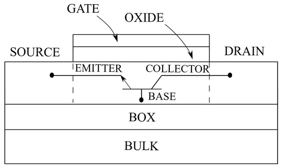
Figure 12.
Parasitic bipolar junction transistor (BJT) in single gate junctionless transistor.
The holes that accumulated in the floating body of the channel can cause a forward bias of the junction associated to the source/channel regions; if this bias turns on the parasitic BJT, then a large leakage current is observed. A possible solution is to employ thin film transistors (Section 3.6), which can reduce the band-to-band-tunneling and, therefore the associated leakage.
3.5. Double Gate
Figure 13 shows the structure of a double gate junctionless transistor. Many models were proposed, and the difference among them depends on the approximations that are involved in the derivation and the considered effects. For instance, many models do not consider short channel and quantum effects [53,55,58,66], while others are only valid for certain doping concentrations and device layer thickness ranges [59,61]. Quantum effects are critically important, because they can affect the threshold voltage [74]. The main issue is modeling the transition between the depletion and the accumulation regions, since the physical behavior is not the same in the two operating regions [56]. A technique involving high doping concentration in the device layer can be considered to reduce the model complexity. This assumption allows for simplifying the depletion width modeling or using the separation of variable in the Poisson equation [62,67].
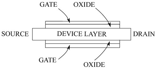
Figure 13.
Cross-sectional view of a double gate junctionless transistor.
A model that describes the current in all of the conduction regimes was proposed in [51]. It was validated for symmetrical long channel DG JLTs and describes the device behavior with a continuous current model. Regarding p-type devices, a threshold voltage model was proposed by [52]. They observed that the threshold voltage increases in absolute value as the device layer thickness, the doping concentration and the oxide thickness are increased. Extracting the threshold voltage and the current is therefore important in order to decide the doping concentration, and the gate oxide and device layer thicknesses [54]. Regarding the device performance, it could be negatively affected by the BTBT, which increases the leakage current. A design choice that improves the performance is the implementation of a thicker gate oxide near the gate edges (Figure 14). It was observed that by modifying the gate oxide structure, the energy bands of the carriers under the gate are modified as well, resulting in a reduction of the leakage current [69].
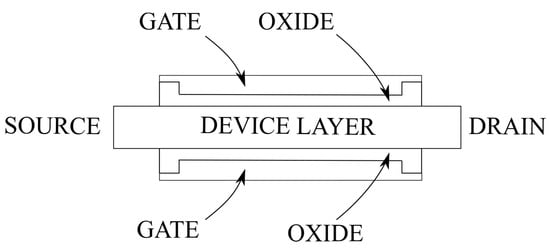
Figure 14.
Modified Double Gate junctionless transistor (DG JLT). The gate oxide is thicker near to the gate edges.
The leakage current is lower in double gate junctionless transistors than in SGJLTs [43]. As reported in Table 3, the DGJLT presents better performance both for uniform and non-uniform (Gaussian) doping concentrations.
Table 3.
Comparison between SGJLT and Double Gate (DGJLT) in terms of for uniform (1 × cm) and non-uniform (Gaussian) doping concentration [43]. is the device layer thickness.
Designers could also implement stacked-oxide structures. When compared to the conventional architecture, they present higher , lower and [57,65]. By choosing a high dielectric constant material (e.g., ), a reduction of the leakage current as well as an improvement of the analog parameters could be observed [63,70]. Besides gate oxide engineering, spacer engineering could lead to a performance improvement. Spacers have an influence on the lateral extension of the depletion width and, therefore, on the effective channel length [72,73]. A simpler approach is doping concentration engineering. It was reported that a concentration of 1 × cm can significantly reduce the threshold voltage sensitivity by 70–90% with respect to the device layer and gate oxide thickness [68]. Graded doping profile can reduce by six orders of magnitude [71]. To correctly model JLTs, it is important to also model the carrier mobilities. The main issue is that the bulk mobility is lower than the accumulation one, because of screening effects. The accumulation mobility can be extracted by taking the second derivative of the curve. The bulk mobility can be computed by knowing the flat band voltage [64]. The mobility values can be degraded in case high voltages are applied [60]. Moreover, the implementation of complex equations (Schrödinger) is required, as well as the knowledge of parameters, such as impurities and surface roughness scattering mechanisms [75].
3.6. Thin Film
Thin film junctionless transistors are characterized by an ultra-thin channel thickness (≤10 nm) and very high doping concentration (≥1 × cm). The thin film is better for obtaining the full depletion in the state, while the high doping concentration ensures high current to flow in the device [77]. An important characteristics of these transistors is their device layer material composition; the majority of reported thin film transistors has polycrystalline silicon as channel material [79,82,84,85]. Therefore, they are identified based on the channel thickness (ultra-thin) and material composition (polysilicon). When considering polysilicon instead of silicon, an important difference arises: the polycrystalline silicon is composed of many crystallites connected by grain boundaries, as shown in Figure 15a. When electrons get trapped in these boundaries (Figure 15b), a space charge potential is formed. The stability of this potential depends on the applied drain voltage. If the latter is too high, trapped electrons could become unstable. The electrons instability influences the grain boundaries potential, which causes oscillation in the drain conductance. This phenomenon is more critical in TFTs with double gates, since the higher mobility allows for the electrons to easily destroy the trapped ones, and increase the oscillation [81]. Designers can limit this phenomenon by increasing the doping concentration [76].
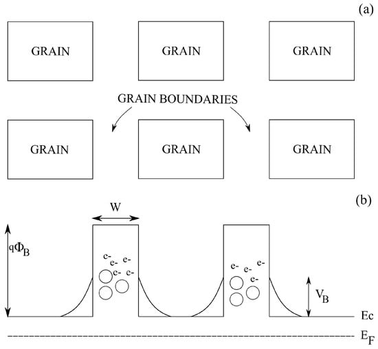
Figure 15.
(a) Crystallites organization in polycrystalline films. (b) Energy band diagram showing the trapped electrons in the grain boundaries.
When compared to junction TFTs, the junctionless ones present smaller transconductance and drain conductance . This implies larger Early voltage, improved low frequency noise and higher signal-to-noise ratio (SNR) [78,83]. The performance of thin film junctionless transistors mainly depends on the film thickness and the doping concentration. A high doping concentration ensures high , but it also lowers the since high carriers concentrations could screen the electric field induced by the gate. The also decreases with reduction in device layer thickness [86]. In addition, the temperature can significantly affect the device performance; when the temperature increases, the threshold voltage decreases (in absolute value) and the increases. This is attributed to the fact that the energy band gap decreases with temperature, thus increasing the carrier concentration [80]. Table 4 presents the figure of merits of the reported thin film junctionless transistors.
Table 4.
Reported figure of merits of junctionless thin film transistors.
3.7. Tunnel FET
Figure 16 shows the structure of a junctionless tunnel field effect transistor. The device is uniformly and highly doped. The middle gate acts as a control gate, while fixed voltages are applied at the side gates. When considering an n-type device, the tunneling effect can be triggered by correctly fixing the voltages on the side gates, where the source, channel, and drain regions (n-n-n) are converted into a (p-i-n) structure. When a certain control voltage is applied, the barrier between the source and the channel becomes narrower. As a result, current flows because of tunneling. Therefore, the conduction mechanism is different with respect to the other JLTs, since it is not based on depletion. The high-k dielectric below the gate (, ) improves the internal electric field, and, thus, the gate control [94]. The low-k spacers (, ) are used to isolate the gates; by increasing the dielectric constant of the low-k spacers, it is possible to reduce [87]. Increasing the device layer doping concentration leads to an increment of both and , with the latter being more sensitive to doping variations. Decreasing the doping concentration leads to an improvement of the , since its value decreases from 290 mV/dec to 47 mV/dec as the doping concentration decreases from 2 × cm to 1 × cm. Therefore, one of the main advantages of junctionless TFETs is the possibility to achieve sub 60 mV/dec . Channel length reductions cause an increment of , and so of the [87].
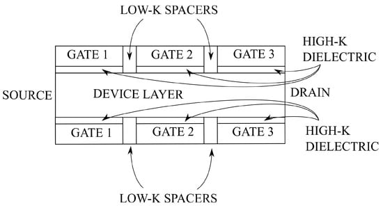
Figure 16.
Cross-sectional view of a junctionless tunnel field effect transistor.
Regarding double gate junctionless TFETs (Figure 17), the increment of the dielectric constant k leads to an improvement of . Increasing the insulation layer thickness causes an improvement in both and . However, this design choice leads to an increment of the parasitic capacitances [88,92]. To improve the robustness of junctionless TFETs, it is possible to selectively introduce dielectric materials in the gate oxide, which can reduce the variations in the coupling capacitance, allowing for higher immunity in terms of sensitivity [93]. The performance can be further increased by implementing dual-material gate (Figure 17a) or heterojunctionless structures (Figure 17b). The energy bandgap of these structures leads to higher and , and lower [89,90,91]. Besides silicon, other materials were used for the device layer: a junctionless TFET made of indium arsenide was proposed [96]. The figure of merits of the reported junctionless transistors are collected in Table 5.
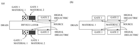
Figure 17.
Cross-sectional view of: (a) JLT Tunnel FET (JLT TFET) with dual-material gate. (b) JLT TFET heterojunctionless.
Table 5.
Reported figure of merits of junctionless tunnel field effect transistors.
4. Conclusions
In this work, junctionless transistors that were proposed over the last decade were studied. In particular, the influence of the technological parameters on the main figure of merits (/, , and ) were analyzed. Design techniques, such as oxide/doping/spacers engineering, have been reported. Depending on the design choices, all of the typologies of junctionless transistors can present a high / ratio, as well as quasi-ideal subthreshold swing and optimal values of . Therefore, it is not possible to determine the best junctionless transistor solely based on the performance parameters. In general, a flexible optimization is associated to the more complex structures. The TFET is difficult to design, since the gate voltages need to be set carefully, and the work function differences must guarantee the tunnel behavior. The DGJLT has a less complex structure compared to TFET, and it presents an additional degree of freedom and enhanced gate control with respect to SGJLT and TFT. The SGJLT has a simple structure, but its performance is not comparable with the other junctionless transistors because of its reduced flexibility in terms of structure engineering. The TFT only presents high performance parameters if the device layer is highly doped and made of very thin polysilicon. FinFETs provide more flexibility in terms of structure engineering as compared to nanowires. The electrostatic control of both nanowires and FinFETs can be increased by surrounding the entire channel with the gate (GAA configuration). Regardless of the structure, junctionless transistors present easier fabrication process and competitive performance when compared to the junction transistors. As junctionless transistors are capable of reaching quasi-ideal subthreshold swing, optimal values, and high / ratio, it is expected that they will replace junction-based electronic devices in the following decade. Junctionless transistors are, therefore, the main candidates to become the conventional field effect transistors of the future.
Author Contributions
Data collection, A.N.; data curation, A.N.; writing—original draft preparation, A.N.; writing—review and editing, A.N., A.R., L.M.; supervision, A.R., L.M.; project administration, L.M. All authors have read and agreed to the published version of the manuscript.
Funding
This research was funded by University of South Eastern Norway.
Conflicts of Interest
The authors declare no conflict of interest. The funders had no role in the design of the study; in the collection, analyses, or interpretation of data; in the writing of the manuscript, or in the decision to publish the results.
Abbreviations
The following abbreviations are used in this manuscript:
| AM | Accumulation Mode |
| BJT | Bipolar Junction Transistor |
| BTBT | Band-To-Band Tunneling |
| BOX | Buried Oxide |
| DG | Double Gate |
| DIBL | Drain-Induced Barrier Lowering |
| FET | Field Effect Transistor |
| GAA | Gate-All-Around |
| IM | Inversion Mode |
| JLT | Junctionless Transistor |
| JT | Junction Transistor |
| LFN | Low Frequency Noise |
| NW | Nanowire |
| SELBOX | Selective Buried Oxide |
| SG | Single Gate |
| SNR | Signal-To-Noise Ratio |
| SOI | Silicon-On-Insulator |
| SON | Silicon-On-Nothing |
| SS | Subthreshold Swing |
| TFET | Tunnel Field Effect Transistor |
| TFT | Thin Film Transistor |
| TG | Triple Gate |
References
- Lilienfeld, J. Method and Apparatus for Controlling Electric Currents. U.S. Patent 1,745,175, 28 January 1930. [Google Scholar]
- Colinge, J.P.; Lee, C.W.; Afzalian, A.; Akhavan, N.D.; Yan, R.; Ferain, I.; Razavi, P.; O’neill, B.; Blake, A.; White, M.; et al. Nanowire transistors without junctions. Nat. Nanotechnol. 2010, 5, 225. [Google Scholar] [CrossRef] [PubMed]
- Rios, R.; Cappellani, A.; Armstrong, M.; Budrevich, A.; Gomez, H.; Pai, R.; Rahhal-Orabi, N.; Kuhn, K. Comparison of junctionless and conventional trigate transistors with Lg down to 26 nm. IEEE Electron. Device Lett. 2011, 32, 1170–1172. [Google Scholar] [CrossRef]
- Han, M.H.; Chang, C.Y.; Chen, H.B.; Cheng, Y.C.; Wu, Y.C. Device and circuit performance estimation of junctionless bulk FinFETs. IEEE Trans. Electron. Devices 2013, 60, 1807–1813. [Google Scholar] [CrossRef]
- Priya, A.; Rai, S.; Mishra, R.A. Comparative analysis of junctionless bulk and SOI/SON FinFET. In Proceedings of the 2017 4th International Conference on Power, Control & Embedded Systems (ICPCES), Allahabad, India, 9–11 March 2017; pp. 1–4. [Google Scholar]
- Han, M.H.; Chang, C.Y.; Chen, H.B.; Wu, J.J.; Cheng, Y.C.; Wu, Y.C. Performance comparison between bulk and SOI junctionless transistors. IEEE Electron. Device Lett. 2013, 34, 169–171. [Google Scholar] [CrossRef]
- Bharathi, R.; Durga, G.; Kumar, N.V.; Nagarajan, K.; Srinivasan, R. Performance optimization of bulk junctionless FinFETs through work function engineering. In Proceedings of the 2014 International Conference on Circuits, Power and Computing Technologies [ICCPCT-2014], Nagercoil, India, 20–21 March 2014; pp. 1291–1295. [Google Scholar]
- Bousari, N.B.; Anvarifard, M.K.; Haji-Nasiri, S. Improving the Electrical Characteristics of Nanoscale Triple-Gate Junctionless FinFET Using Gate Oxide Engineering. AEU Int. J. Electron. Commun. 2019, 108, 226–234. [Google Scholar] [CrossRef]
- Saini, G.; Choudhary, S. Improving the subthreshold performance of junctionless transistor using spacer engineering. Microelectron. J. 2017, 59, 55–58. [Google Scholar] [CrossRef]
- Kaundal, S.; Rana, A.K. Design and structural optimization of junctionless FinFET with Gaussian-doped channel. J. Comput. Electron. 2018, 17, 637–645. [Google Scholar] [CrossRef]
- Pal, P.K.; Nehra, D.; Kaushik, B.K.; Dasgupta, S. Enhanced device performance using lightly doped channel junctionless accumulation-mode FinFET. In Proceedings of the 2015 12th International Conference on Electrical Engineering/Electronics, Computer, Telecommunications and Information Technology (ECTI-CON), Hua Hin, Thailand, 24–27 June 2015; pp. 1–5. [Google Scholar]
- Bharti, S.; Saini, G. Sensitivity Analysis of Junctionless FinFET for Analog Applications. In Proceedings of the 2018 Second International Conference on Intelligent Computing and Control Systems (ICICCS), Madurai, India, 14–15 June 2018; pp. 1288–1293. [Google Scholar]
- Kaundal, S.; Rana, A.K. Threshold voltage modeling for a Gaussian-doped junctionless FinFET. J. Comput. Electron. 2019, 18, 83–90. [Google Scholar] [CrossRef]
- Tayal, S.; Nandi, A. Analog/RF performance analysis of channel engineered high-k gate-stack based junctionless trigate-FinFET. Superlattices Microstruct. 2017, 112, 287–295. [Google Scholar] [CrossRef]
- Lü, W.F.; Dai, L. Impact of work-function variation on analog figures-of-merits for high-k/metal-gate junctionless FinFET and gate-all-around nanowire MOSFET. Microelectron. J. 2019, 84, 54–58. [Google Scholar] [CrossRef]
- Dwivedi, S.; Saini, G. Effect of random dopant fluctuation in nanoscale junctionless FinFET using low and high-k spacers. In Proceedings of the 2017 8th International Conference on Computing, Communication and Networking Technologies (ICCCNT), Delhi, India, 3–5 July 2017; pp. 1–4. [Google Scholar]
- Nawaz, S.M.; Dutta, S.; Chattopadhyay, A.; Mallik, A. Comparison of random dopant and gate-metal workfunction variability between junctionless and conventional FinFETs. IEEE Electron. Device Lett. 2014, 35, 663–665. [Google Scholar]
- Nawaz, S.M.; Mallik, A. Effects of device scaling on the performance of junctionless FinFETs due to gate-metal work function variability and random dopant fluctuations. IEEE Electron. Device Lett. 2016, 37, 958–961. [Google Scholar] [CrossRef]
- Jegadheesan, V.; Sivasankaran, K. RF stability performance of SOI junctionless FinFET and impact of process variation. Microelectron. J. 2017, 59, 15–21. [Google Scholar] [CrossRef]
- Liu, F.Y.; Liu, H.Z.; Liu, B.W.; Guo, Y.F. An analytical model for nanowire junctionless SOI FinFETs with considering three-dimensional coupling effect. Chin. Phys. B 2016, 25, 47305. [Google Scholar] [CrossRef]
- Kumar, A.; Chhabra, A.; Chaujar, R. GaAs Junctionless FinFET Using High-k Dielectric for High-Performance Applications. In Proceedings of the 2018 IEEE 38th International Conference on Electronics and Nanotechnology (ELNANO), Kiev, Ukraine, 24–26 April 2018; pp. 126–129. [Google Scholar]
- Lee, J.; Kim, Y.; Cho, S. Design of poly-Si junctionless fin-channel FET with quantum-mechanical drift-diffusion models for sub-10-nm technology nodes. IEEE Trans. Electron. Devices 2016, 63, 4610–4616. [Google Scholar] [CrossRef]
- Chang, P.C.; Hsiao, C.J.; Lumbantoruan, F.J.; Wu, C.H.; Lin, Y.K.; Lin, Y.C.; Sze, S.M.; Chang, E.Y. InGaAs Junctionless FinFETs With Self-Aligned Ni-InGaAs S/D. IEEE J. Electron. Devices Soc. 2018, 6, 856–860. [Google Scholar] [CrossRef]
- Djeffal, F.; Ferhati, H.; Bentrcia, T. Improved analog and RF performances of gate-all-around junctionless MOSFET with drain and source extensions. Superlattices Microstruct. 2016, 90, 132–140. [Google Scholar] [CrossRef]
- Moon, D.I.; Choi, S.J.; Duarte, J.P.; Choi, Y.K. Investigation of silicon nanowire gate-all-around junctionless transistors built on a bulk substrate. IEEE Trans. Electron. Devices 2013, 60, 1355–1360. [Google Scholar] [CrossRef]
- Sharma, M.; Gupta, M.; Narang, R.; Saxena, M. Investigation of Gate All Around Junctionless Nanowire Transistor with Arbitrary Polygonal Cross Section. In Proceedings of the 2018 4th International Conference on Devices, Circuits and Systems (ICDCS), Coimbatore, India, 16–17 March 2018; pp. 159–163. [Google Scholar]
- Nobrega, R.; Fonseca, Y.; A Costa, R.; Duarte, U. Comparative Study on the Performance of Silicon and III-V Nanowire Gate-All-Around Field-Effect Transistors for Different Gate Oxides. In Proceedings of the XIII Workshop on Semiconductors and Micro & Nano Technology, São Bernardo do Campo, Brazil, 19–20 April 2018. [Google Scholar]
- Singh, P.; Singh, N.; Miao, J.; Park, W.T.; Kwong, D.L. Gate-all-around junctionless nanowire MOSFET with improved low-frequency noise behavior. IEEE Electron. Device Lett. 2011, 32, 1752–1754. [Google Scholar] [CrossRef]
- Sharma, S. An Extensive Evaluation of Futuristic Gate All Around Junctionless Nanowire MOSFET Using Numerical Simulation. Int. J. Res. Appl. Sci. Eng. Technol. 2017, V, 1974–1979. [Google Scholar] [CrossRef]
- Han, M.H.; Chang, C.Y.; Jhan, Y.R.; Wu, J.J.; Chen, H.B.; Cheng, Y.C.; Wu, Y.C. Characteristic of p-type junctionless gate-all-around nanowire transistor and sensitivity analysis. IEEE Electron. Device Lett. 2013, 34, 157–159. [Google Scholar] [CrossRef]
- Lime, F.; Ávila-Herrera, F.; Cerdeira, A.; Iñiguez, B. A compact explicit DC model for short channel Gate-All-Around junctionless MOSFETs. Solid State Electron. 2017, 131, 24–29. [Google Scholar] [CrossRef]
- Ferhati, H.; Djeffal, F.; Bentrcia, T. Investigation of analog/RF performance of gate-all-around junctionless MOSFET including interfacial defects. In Proceedings of the 2015 4th International Conference on Electrical Engineering (ICEE), Boumerdes, Algeria, 13–15 December 2015; pp. 1–4. [Google Scholar]
- Liu, T.Y.; Pan, F.M.; Sheu, J.T. Characteristics of gate-all-around junctionless polysilicon nanowire transistors with twin 20-nm gates. IEEE J. Electron. Devices Soc. 2015, 3, 405–409. [Google Scholar] [CrossRef]
- Pratap, Y.; Gautam, R.; Haldar, S.; Gupta, R.; Gupta, M. Physics-based drain current modeling of gate-all-around junctionless nanowire twin-gate transistor (JN-TGT) for digital applications. J. Comput. Electron. 2016, 15, 492–501. [Google Scholar] [CrossRef]
- Kumar, P.; Singh, S.; Singh, N.P.; Modi, B.; Gupta, N. Germanium v/s silicon Gate-all-around junctionless nanowire transistor. In Proceedings of the 2014 2nd International Conference on Devices, Circuits and Systems (ICDCS), Combiatore, India, 6–8 March 2014; pp. 1–5. [Google Scholar]
- Sung, P.J.; Cho, T.C.; Chen, P.C.; Hou, F.J.; Lai, C.H.; Lee, Y.J.; Li, Y.; Samukawa, S.; Chao, T.S.; Wu, W.F.; et al. High performance silicon N-channel gate-all-around junctionless field effect transistors by strain technology. In Proceedings of the 2016 IEEE 16th International Conference on Nanotechnology (IEEE-NANO), Sendai, Japan, 22–25 August 2016; pp. 174–175. [Google Scholar]
- Arefín, U.A. Impact of Temperature on Threshold Voltage of Gate-All-Around Junctionless Nanowire Field-Effect Transistor. ULAB J. Sci. Eng. 2015, 6, 14–18. [Google Scholar]
- Gundapaneni, S.; Ganguly, S.; Kottantharayil, A. Bulk planar junctionless transistor (BPJLT): An attractive device alternative for scaling. IEEE Electron. Device Lett. 2011, 32, 261–263. [Google Scholar] [CrossRef]
- Baruah, R.K.; Paily, R.P. Analog performance of bulk planar junctionless transistor (BPJLT). In Proceedings of the 2012 Third International Conference on Computing, Communication and Networking Technologies (ICCCNT’12), Coimbatore, India, 26–28 July 2012; pp. 1–4. [Google Scholar]
- Baruah, R.K.; Paily, R.P. Impact of active well biasing on process-induced variations of a bulk planer junctionless transistor. In Proceedings of the 2016 3rd International Conference on Emerging Electronics (ICEE), Mumbai, India, 27–30 December 2016; pp. 1–4. [Google Scholar]
- Jenifer, I.; Vinodhkumar, N.; Srinivasan, R. Optimization of Bulk Planar Junctionless Transistor using Work function, Device layer thickness and Channel doping concentration with OFF Current constraint. In Proceedings of the 2016 Online International Conference on Green Engineering and Technologies (IC-GET), Coimbatore, India, 19 November 2016; pp. 1–3. [Google Scholar]
- Huda, A.; Arshad, M.M.; Othman, N.; Voon, C.; Ayub, R.; Gopinath, S.C.; Foo, K.; Ruslinda, A.; Hashim, U.; Lee, H.C.; et al. Impact of size variation in junctionless vs junction planar SOI n-MOSFET transistor. In Proceedings of the 2015 IEEE Regional Symposium on Micro and Nanoelectronics (RSM), Kuala Terengganu, Malaysia, 19–21 August 2015; pp. 1–4. [Google Scholar]
- Singh, D.K.; Kumar, P.K.; Akram, M. Investigation of Planar and Double-Gate Junctionless Transistors with Non-Uniform Doping. In Proceedings of the 2018 5th IEEE Uttar Pradesh Section International Conference on Electrical, Electronics and Computer Engineering (UPCON), Gorakhpur, India, 2–4 November 2018; pp. 1–5. [Google Scholar]
- Scarlet, S.P.; Srinivasan, R. Impact of Doping and Spacer on the Performance of Bulk Planar Junctionless devices. In Proceedings of the 2018 4th International Conference on Electrical Energy Systems (ICEES), Chennai, India, 7–9 February 2018; pp. 267–273. [Google Scholar]
- Gundapaneni, S.; Ganguly, S.; Kottantharayil, A. Enhanced Electrostatic Integrity of Short-Channel Junctionless Transistor With High-k Spacers. IEEE Electron. Device Lett. 2011, 32, 1325–1327. [Google Scholar] [CrossRef]
- Ramarao, G.; Ghosekar, I.C.; Patil, G.C. Dual-k HfO 2 Spacer Bulk Planar Junctionless Transistor for Sub-30 nm Low Power CMOS. In Proceedings of the 2017 14th IEEE India Council International Conference (INDICON), Roorkee, India, 15–17 December 2017; pp. 1–4. [Google Scholar]
- Parihar, M.S.; Liu, F.; Navarro, C.; Barraud, S.; Bawedin, M.; Ionica, I.; Kranti, A.; Cristoloveanu, S. Back-gate effects and mobility characterization in junctionless transistor. Solid State Electron. 2016, 125, 154–160. [Google Scholar] [CrossRef]
- Khan, U.; Ghosh, B.; Akram, M.W.; Salimath, A. A comparative study of SELBOX-JLT and SOI-JLT. Appl. Phys. A 2014, 117, 2281–2288. [Google Scholar] [CrossRef]
- Gundapaneni, S.; Bajaj, M.; Pandey, R.K.; Murali, K.V.; Ganguly, S.; Kottantharayil, A. Effect of band-to-band tunneling on junctionless transistors. IEEE Trans. Electron. Devices 2012, 59, 1023–1029. [Google Scholar] [CrossRef]
- Ehteshamuddin, M.; Loan, S.A.; Rafat, M. Planar junctionless silicon-on-insulator transistor with buried metal layer. IEEE Electron. Device Lett. 2018, 39, 799–802. [Google Scholar] [CrossRef]
- Lin, X.; Zhang, B.; Xiao, Y.; Lou, H.; Zhang, L.; Chan, M. Analytical current model for long-channel junctionless double-gate MOSFETs. IEEE Trans. Electron. Devices 2016, 63, 959–965. [Google Scholar] [CrossRef]
- Adnan, M.M.R.; Khosru, Q.D.M. A Simple Analytical Model of Threshold Voltage for P-Channel Double Gate Junctionless Transistor. In Proceedings of the 2018 IEEE International Conference on Electron, Devices and Solid State Circuits (EDSSC), Shenzhen, China, 6–8 June 2018; pp. 1–5. [Google Scholar]
- Bora, N.; Das, P.; Subadar, R. An Analytical Universal Model for Symmetric Double Gate Junctionless Transistors. J. Nano Electron. Phys. 2016, 8, 02003-1. [Google Scholar] [CrossRef]
- Ding, Z.; Hu, G.; Liu, R.; Wang, L.; Hu, S.; Zhou, X. Analytical models for the electric potential, threshold voltage and drain current of long-channel junctionless double-gate transistors. J. Korean Phys. Soc. 2013, 62, 1188–1193. [Google Scholar] [CrossRef]
- Yesayan, A.; Prégaldiny, F.; Sallese, J.M. Explicit drain current model of junctionless double-gate field-effect transistors. Solid State Electron. 2013, 89, 134–138. [Google Scholar] [CrossRef]
- Ávila-Herrera, F.; Cerdeira, A.; Paz, B.; Estrada, M.; Íñiguez, B.; Pavanello, M. Compact model for short-channel symmetric double-gate junctionless transistors. Solid State Electron. 2015, 111, 196–203. [Google Scholar] [CrossRef]
- Fabiha, R.; Saha, C.N.; Islam, M.S. Analytical modeling and performance analysis for symmetric double gate stack-oxide junctionless field effect transistor in subthreshold region. In Proceedings of the 2017 IEEE Region 10 Humanitarian Technology Conference (R10-HTC), Dhaka, Bangladesh, 21–23 December 2017; pp. 310–313. [Google Scholar]
- Chen, Z.; Xiao, Y.; Tang, M.; Xiong, Y.; Huang, J.; Li, J.; Gu, X.; Zhou, Y. Surface-potential-based drain current model for long-channel junctionless double-gate MOSFETs. IEEE Trans. Electron. Devices 2012, 59, 3292–3298. [Google Scholar] [CrossRef]
- Cerdeira, A.; Estrada, M.; Iniguez, B.; Trevisoli, R.; Doria, R.; de Souza, M.; Pavanello, M. Charge-based continuous model for long-channel symmetric double-gate junctionless transistors. Solid State Electron. 2013, 85, 59–63. [Google Scholar] [CrossRef]
- Paz, B.; Ávila-Herrera, F.; Cerdeira, A.; Pavanello, M. Double-gate junctionless transistor model including short-channel effects. Semicond. Sci. Technol. 2015, 30, 055011. [Google Scholar] [CrossRef]
- Cerdeira, A.; Ávila, F.; Íñiguez, B.; De Souza, M.; Pavanello, M.; Estrada, M. Compact core model for symmetric double-gate junctionless transistors. Solid State Electron. 2014, 94, 91–97. [Google Scholar] [CrossRef]
- Duarte, J.P.; Choi, S.J.; Moon, D.I.; Choi, Y.K. Simple analytical bulk current model for long-channel double-gate junctionless transistors. IEEE Electron. Device Lett. 2011, 32, 704–706. [Google Scholar] [CrossRef]
- Amin, S.I.; Sarin, R. Direct tunneling gate current model for symmetric double gate junctionless transistor with SiO2/high-k gate stacked dielectric. J. Semicond. 2016, 37, 034001. [Google Scholar] [CrossRef]
- Bhuvaneshwari, Y.; Kranti, A. Extraction of mobility and degradation coefficients in double gate junctionless transistors. Semicond. Sci. Technol. 2017, 32, 125011. [Google Scholar] [CrossRef]
- Islam, M.S.; Afza, J.; Tarannum, S. Modelling and performance analysis of asymmetric double gate stack-oxide junctionless FET in subthreshold region. In Proceedings of the 2017 IEEE Region 10 Humanitarian Technology Conference (R10-HTC), Dhaka, Bangladesh, 21–23 December 2017; pp. 538–541. [Google Scholar]
- Chowdhury, S.; Khan, M.Z.R. Surface potential modeling of Junctionless Double Gate MOSFETs using gradual depletion approximation. In Proceedings of the 8th International Conference on Electrical and Computer Engineering, Dhaka, Bangladesh, 20–22 December 2014; pp. 108–111. [Google Scholar]
- Jin, X.; Liu, X.; Wu, M.; Chuai, R.; Lee, J.H.; Lee, J.H. Modelling of the nanoscale channel length effect on the subthreshold characteristics of junctionless field-effect transistors with a symmetric double-gate structure. J. Phys. Appl. Phys. 2012, 45, 375102. [Google Scholar] [CrossRef]
- Parihar, M.S.; Kranti, A. Revisiting the doping requirement for low power junctionless MOSFETs. Semicond. Sci. Technol. 2014, 29, 075006. [Google Scholar] [CrossRef]
- Wu, M.; Jin, X.; Kwon, H.I.; Chuai, R.; Liu, X.; Lee, J.H. The optimal design of junctionless transistors with double-gate structure for reducing the effect of band-to-band tunneling. J. Semicond. Technol. Sci. 2013, 13, 245–251. [Google Scholar] [CrossRef]
- Baidya, A.; Baishya, S.; Lenka, T.R. Impact of thin high-k dielectrics and gate metals on RF characteristics of 3D double gate junctionless transistor. Mater. Sci. Semicond. Process. 2017, 71, 413–420. [Google Scholar] [CrossRef]
- Bal, P.; Ghosh, B.; Mondal, P.; Akram, M. A laterally graded junctionless transistor. J. Semicond. 2014, 35, 034003. [Google Scholar] [CrossRef]
- Mandia, A.; Rana, A. Performance Enhancement of Double Gate Junctionless Transistor Using High-K Spacer and Models. In Proceedings of the 11th IRF International Conference, Delhi, India, 25 May 2014; Volume 8, pp. 8–11. [Google Scholar]
- Gupta, M.; Kranti, A. Sidewall spacer optimization for steep switching junctionless transistors. Semicond. Sci. Technol. 2016, 31, 065017. [Google Scholar] [CrossRef]
- Chen, C.Y.; Lin, J.T.; Chiang, M.H. Threshold-voltage variability analysis and modeling for junctionless double-gate transistors. Microelectron. Reliab. 2017, 74, 22–26. [Google Scholar] [CrossRef]
- Chen, F.; Wei, K.; Wei, E.; Huang, J.Z. Hole mobility model for Si double-gate junctionless transistors. In Proceedings of the 2017 IEEE Electrical Design of Advanced Packaging and Systems Symposium (EDAPS), Haining, China, 14–16 December 2017; pp. 1–3. [Google Scholar]
- Lin, H.C.; Lin, C.I.; Huang, T.Y. Characteristics of n-type junctionless poly-Si thin-film transistors with an ultrathin channel. IEEE Electron. Device Lett. 2011, 33, 53–55. [Google Scholar] [CrossRef]
- Lin, H.C.; Lin, C.I.; Lin, Z.M.; Shie, B.S.; Huang, T.Y. Characteristics of planar junctionless poly-Si thin-film transistors with various channel thickness. IEEE Trans. Electron. Devices 2013, 60, 1142–1148. [Google Scholar] [CrossRef]
- Wang, S.W.; Lin, J.T.; Eng, Y.C.; Chang, Y.C.; Lin, C.H.; Chen, H.H.; Lin, P.H.; Tai, C.H.; Pai, C.Y. A qualitative comparison study of analog performance of junction and junctionless poly-Si TFTs. In Proceedings of the 2011 IEEE International Conference of Electron. Devices and Solid-State Circuits, Tianjin, China, 17–18 November 2011; pp. 1–2. [Google Scholar]
- Chou, C.H.; Lee, I.C.; Lei, D.C.; Cheng, H.C. Planar junctionless poly-Si thin-film transistors with single gate and double gate. Jpn. J. Appl. Phys. 2014, 53, 06JE07. [Google Scholar] [CrossRef]
- Cheng, Y.C.; Chen, H.B.; Su, J.J.; Shao, C.S.; Wang, C.P.; Chang, C.Y.; Wu, Y.C. Characterizing the electrical properties of raised S/D junctionless thin-film transistors with a dual-gate structure. Nanoscale Res. Lett. 2014, 9, 669. [Google Scholar] [CrossRef] [PubMed]
- Kang, T.K.; Peng, Y.H. Drain Conductance Oscillations in Poly-Si Junctionless Nanowire Thin-Film Transistors. IEEE Trans. Electron. Devices 2018, 66, 451–456. [Google Scholar] [CrossRef]
- Su, C.J.; Tsai, T.I.; Liou, Y.L.; Lin, Z.M.; Lin, H.C.; Chao, T.S. Gate-all-around junctionless transistors with heavily doped polysilicon nanowire channels. IEEE Electron. Device Lett. 2011, 32, 521–523. [Google Scholar] [CrossRef]
- Tsai, T.I.; Chen, K.M.; Lin, H.C.; Lin, T.Y.; Su, C.J.; Chao, T.S.; Huang, T.Y. Low-operating-voltage ultrathin junctionless poly-Si thin-film transistor technology for RF applications. IEEE Electron. Device Lett. 2012, 33, 1565–1567. [Google Scholar] [CrossRef]
- Chen, H.B.; Wu, Y.C.; Chang, C.Y.; Han, M.H.; Lu, N.H.; Cheng, Y.C. Performance of GAA poly-Si nanosheet (2 nm) channel of junctionless transistors with ideal subthreshold slope. In Proceedings of the 2013 Symposium on VLSI Technology, Kyoto, Japan, 11–13 June 2013; pp. T232–T233. [Google Scholar]
- Thirunavukkarasu, V.; Jhan, Y.R.; Liu, Y.B.; Kurniawan, E.D.; Lin, Y.R.; Yang, S.Y.; Cheng, C.H.; Wu, Y.C. Gate-all-around junctionless silicon transistors with atomically thin nanosheet channel (0.65 nm) and record sub-threshold slope (43 mV/dec). Appl. Phys. Lett. 2017, 110, 032101. [Google Scholar] [CrossRef]
- Ma, W.C.Y.; Wang, J.Y.; Wang, H.C.; Huang, Y.J.; Yu, L.W. Dependence of Sub-Thermionic Swing on Channel Thickness and Drain Bias of Poly-Si Junctionless Thin-Film Transistor. IEEE Electron. Device Lett. 2018, 39, 1122–1125. [Google Scholar] [CrossRef]
- Ghosh, B.; Bal, P.; Mondal, P. A junctionless tunnel field effect transistor with low subthreshold slope. J. Comput. Electron. 2013, 12, 428–436. [Google Scholar] [CrossRef]
- Ghosh, B.; Akram, M.W. Junctionless tunnel field effect transistor. IEEE Electron. Device Lett. 2013, 34, 584–586. [Google Scholar] [CrossRef]
- Asthana, P.K.; Ghosh, B.; Goswami, Y.; Tripathi, B.M.M. High-speed and low-power ultradeep-submicrometer III-V heterojunctionless tunnel field-effect transistor. IEEE Trans. Electron. Devices 2014, 61, 479–486. [Google Scholar] [CrossRef]
- Rahi, S.B.; Ghosh, B.; Asthana, P. A simulation-based proposed high-k heterostructure AlGaAs/Si junctionless n-type tunnel FET. J. Semicond. 2014, 35, 114005. [Google Scholar] [CrossRef]
- Rahi, S.B.; Ghosh, B.; Bishnoi, B. Temperature effect on hetero structure junctionless tunnel FET. J. Semicond. 2015, 36, 034002. [Google Scholar] [CrossRef]
- Akram, M.; Ghosh, B.; Bal, P.; Mondal, P. P-type double gate junctionless tunnel field effect transistor. J. Semicond. 2014, 35, 014002. [Google Scholar] [CrossRef]
- Gupta, S.; Nigam, K.; Pandey, S.; Sharma, D.; Kondekar, P.N. Effect of interface trap charges on performance variation of heterogeneous gate dielectric junctionless-TFET. IEEE Trans. Electron. Devices 2017, 64, 4731–4737. [Google Scholar] [CrossRef]
- Rahi, S.B.; Asthana, P.; Gupta, S. Heterogate junctionless tunnel field-effect transistor: Future of low-power devices. J. Comput. Electron. 2017, 16, 30–38. [Google Scholar] [CrossRef]
- Bal, P.; Akram, M.; Mondal, P.; Ghosh, B. Performance estimation of sub-30 nm junctionless tunnel FET (JLTFET). J. Comput. Electron. 2013, 12, 782–789. [Google Scholar] [CrossRef]
- Asthana, P.K.; Goswami, Y.; Ghosh, B. A novel sub 20 nm single gate tunnel field effect transistor with intrinsic channel for ultra low power applications. J. Semicond. 2016, 37, 054002. [Google Scholar] [CrossRef]
- Priya, G.L.; Balamurugan, N. New dual material double gate junctionless tunnel FET: Subthreshold modeling and simulation. AEU Int. J. Electron. Commun. 2019, 99, 130–138. [Google Scholar] [CrossRef]
- Solankia, T.; Parmar, N. A Review paper: A Comprehensive study of Junctionless transistor. In Proceedings of the National Conference on Recent Trends in Engineering & Technology, Kerala, India, 25–26 February 2011; pp. 13–14. [Google Scholar]
- Amin, S.I.; Sarin, R. Junctionless Transistor: A Review; IET: London, UK, 2013. [Google Scholar]
- Sahu, S.R.; Agrawal, R.S.; Balwani, S.M. Review of Junctionless transistor using CMOS technology and MOSFETs. Int. J. Comput. Appl. 2012, 2012, 8–11. [Google Scholar]
- Das, S.; Kundu, S. A Review on Junctionless Transistor-A Prospective sub-10nm Logic Device. Adv. Res. Electr. Electron. Eng. 2014, 1, 98–102. [Google Scholar]
- Jyoti Ligira, P.; Khanna, G. Review on Different Types of Junctionless Transistors. 2014. Available online: https://www.semanticscholar.org/paper/Review-on-different-types-of-Junctionless-Ligira-Khanna/5495a666cabde857e7a3fd08ae7de935a7acef5e (accessed on 23 June 2020).
- Xu, W.; Rhee, S.W. Hysteresis-free organic field-effect transistors with high dielectric strength cross-linked polyacrylate copolymer as a gate insulator. Org. Electron. 2010, 11, 836–845. [Google Scholar] [CrossRef]
- Xu, W.; Rhee, S.W. Organic field-effect transistors with cross-linked high-k cyanoethylated pullulan polymer as a gate insulator. Org. Electron. 2010, 11, 996–1004. [Google Scholar] [CrossRef]
- Ni, Y.; Zhou, J.; Hao, Y.; Yu, H.; Li, Y.; Ruan, Z.; Gan, P. Effective performance improvement of organic thin film transistors by using tri-layer insulators. Eur. Phys. J. Appl. Phys. 2018, 83, 20201. [Google Scholar] [CrossRef]
- Xu, W.; Guo, C.; Rhee, S.W. High performance organic field-effect transistors using cyanoethyl pullulan (CEP) high-k polymer cross-linked with trimethylolpropane triglycidyl ether (TTE) at low temperatures. J. Mater. Chem. C 2013, 1, 3955–3960. [Google Scholar] [CrossRef]
- Jiang, J.; Wan, Q.; Zhang, Q. Transparent junctionless electric-double-layer transistors gated by a reinforced chitosan-based biopolymer electrolyte. IEEE Trans. Electron. Devices 2013, 60, 1951–1957. [Google Scholar] [CrossRef]
- Jiang, J.; Wan, Q.; Sun, J.; Dou, W.; Zhang, Q. Gated Conductance of Thin Indium Tin Oxide-The Simplest Transistor. arXiv 2012, arXiv:1204.0169. [Google Scholar]
- Liu, Q.; Sakurai, T.; Hiramoto, T. Optimum device consideration for standby power reduction scheme using drain-induced barrier lowering. Jpn. J. Appl. Phys. 2003, 42, 2171. [Google Scholar] [CrossRef]
- Sze, S.M.; Ng, K.K. Physics of Semiconductor Devices; John Wiley & Sons: Hoboken, NJ, USA, 2006. [Google Scholar]
- Colinge, J.P.; Lee, C.W.; Afzalian, A.; Dehdashti, N.; Yan, R.; Ferain, I.; Razavi, P.; O’Neill, B.; Blake, A.; White, M.; et al. SOI gated resistor: CMOS without junctions. In Proceedings of the 2009 IEEE International SOI Conference, Foster City, CA, USA, 5–8 October 2009; pp. 1–2. [Google Scholar]
- Ionescu, A.M. Electronic devices: Nanowire transistors made easy. Nat. Nanotechnol. 2010, 5, 178. [Google Scholar] [CrossRef]
- Kranti, A.; Yan, R.; Lee, C.W.; Ferain, I.; Yu, R.; Akhavan, N.D.; Razavi, P.; Colinge, J. Junctionless nanowire transistor (JNT): Properties and design guidelines. In Proceedings of the 2010 Proceedings of the European Solid State Device Research Conference, Sevilla, Spain, 14–16 September 2010; pp. 357–360. [Google Scholar]
- Yu, Y.S.; Lee, S.H.; Oh, J.H.; Kim, H.J.; Hwang, S.W.; Ahn, D. A compact analytical current conduction model for a depletion-mode n-type nanowire field-effect transistor with a bottom-gate structure. Semicond. Sci. Technol. 2008, 23, 035025. [Google Scholar] [CrossRef]
- Yu, Y.S. A semi-analytical model for depletion-mode N-type nanowire field-effect transistor (NWFET) with top-gate structure. J. Semicond. Technol. Sci. 2010, 10, 152–159. [Google Scholar] [CrossRef][Green Version]
- Trevisoli, R.D.; Doria, R.T.; de Souza, M.; Pavanello, M.A. A physically-based threshold voltage definition, extraction and analytical model for junctionless nanowire transistors. Solid State Electron. 2013, 90, 12–17. [Google Scholar] [CrossRef]
- Trevisoli, R.D.; Doria, R.T.; de Souza, M.; Pavanello, M.A. Threshold voltage in junctionless nanowire transistors. Semicond. Sci. Technol. 2011, 26, 105009. [Google Scholar] [CrossRef]
- Lim, B.; Arshad, M.M.; Othman, N.; Fathil, M.; Fatin, M.; Hashim, U. The impact of channel doping in junctionless field effect transistor. In Proceedings of the 2014 IEEE International Conference on Semiconductor Electronics (ICSE2014), Kuala Lumpur, Malaysia, 27–29 August 2014; pp. 112–114. [Google Scholar]
- Joo, M.K.; Mouis, M.; Jeon, D.Y.; Barraud, S.; Park, S.J.; Kim, G.T.; Ghibaudo, G. Flat-band voltage and low-field mobility analysis of junctionless transistors under low-temperature. Semicond. Sci. Technol. 2014, 29, 045024. [Google Scholar] [CrossRef]
- Trevisoli, R.; De Souza, M.; Doria, R.T.; Kilchtyska, V.; Flandre, D.; Pavanello, M.A. Junctionless nanowire transistors operation at temperatures down to 4.2 K. Semicond. Sci. Technol. 2016, 31, 114001. [Google Scholar] [CrossRef]
- Trevisoli, R.; Doria, R.; De Souza, M.; Pavanello, M. Accounting for Series Resistance in the Compact Model of Triple-Gate Junctionless Nanowire Transistors. In Proceedings of the 2018 33rd Symposium on Microelectronics Technology and Devices (SBMicro), Bento Goncalves, Brazil, 27–31 August 2018; pp. 1–4. [Google Scholar]
- Trevisoli, R.; Trevisoli Doria, R.; de Souza, M.; Antonio Pavanello, M. Analysis of the leakage current in junctionless nanowire transistors. Appl. Phys. Lett. 2013, 103, 202103. [Google Scholar] [CrossRef]
- Oproglidis, T.; Karatsori, T.; Barraud, S.; Ghibaudo, G.; Dimitriadis, C. Leakage current conduction in metal gate junctionless nanowire transistors. Solid State Electron. 2017, 131, 20–23. [Google Scholar] [CrossRef]
- Colinge, J.P.; Lee, C.W.; Ferain, I.; Akhavan, N.D.; Yan, R.; Razavi, P.; Yu, R.; Nazarov, A.N.; Doria, R.T. Reduced electric field in junctionless transistors. Appl. Phys. Lett. 2010, 96, 073510. [Google Scholar] [CrossRef]
- Rudenko, T.; Nazarov, A.; Yu, R.; Barraud, S.; Cherkaoui, K.; Razavi, P.; Fagas, G. Electron mobility in heavily doped junctionless nanowire SOI MOSFETs. Microelectron. Eng. 2013, 109, 326–329. [Google Scholar] [CrossRef]
- Sun, C.; Liang, R.; Xiao, L.; Liu, L.; Xu, J.; Wang, J. Cryogenic Characteristics of Ge channel Junctionless Nanowire Transistors. In Proceedings of the 2018 IEEE 2nd Electron. Devices Technology and Manufacturing Conference (EDTM), Kobe, Japan, 13–16 March 2018; pp. 286–288. [Google Scholar]
- Razavi, P.; Fagas, G.; Ferain, I.; Yu, R.; Das, S.; Colinge, J.P. Influence of channel material properties on performance of nanowire transistors. J. Appl. Phys. 2012, 111, 124509. [Google Scholar] [CrossRef]
- Trevisoli, R.; Doria, R.T.; de Souza, M.; Pavanello, M.A.; Barraud, S.; Vinet, M. Influence of the crystal orientation on the operation of junctionless nanowire transistors. In Proceedings of the 2016 IEEE SOI-3D-Subthreshold Microelectronics Technology Unified Conference (S3S), Burlingame, CA, USA, 10–13 October 2016; pp. 1–3. [Google Scholar]


© 2020 by the authors. Licensee MDPI, Basel, Switzerland. This article is an open access article distributed under the terms and conditions of the Creative Commons Attribution (CC BY) license (http://creativecommons.org/licenses/by/4.0/).