Article

Fast Logic Function Extraction of LUT from Bitstream in Xilinx FPGA

Department of Electronics Engineering, Chungnam National University, Daejeon 34134, Korea
*
Author to whom correspondence should be addressed.
Electronics 2020, 9(7), 1132; https://doi.org/10.3390/electronics9071132
Submission received: 12 June 2020 / Revised: 29 June 2020 / Accepted: 9 July 2020 / Published: 11 July 2020
(This article belongs to the Section Circuit and Signal Processing)

Abstract

:
This paper presents a fast method to extract logic functions of look-up tables (LUTs) from a bitstream in Xilinx FPGAs. In general, FPGAs utilize LUTs as a primary resource to realize a logic function, and a typical N-input LUT comprises 2N 1-bit SRAM and N – 1 multiplexers. Whereas the previous research demands 2N exhaustive processing to find a mapping rule between an LUT and a bitstream, the proposed method decreases the processing to 2N by eliminating unnecessary processing. Experimental results show that the proposed method can reduce reversing time by more than 57% and 85% for Xilinx Spartan-3 and Virtex-5 compared to the previous exhaustive algorithm. It is noticeable that the reduction time becomes more significant as a commercial Xilinx FPGA tends to include a more tremendous number of LUTs.

1. Introduction

Field programmable gate arrays (FPGAs) are a type of semiconductor device that can be reconfigured by register transfer level (RTL) designers to realize target functionality. A typical FPGA conceptually consists of a tile of three major blocks [1,2], configurable logic blocks (CLBs), input/output blocks (IOBs), and switch matrices (SMs), as shown in Figure 1. CLB is a primary resource to realize target logic function. Each CLB is decomposed into several SLICEs, each of which contains look-up-tables (LUTs), flip-flops (FFs), and multiplexes (MUXs). In addition, IOBs are responsible for controlling external connectivity and SMs provide configurable internal connectivity between the CLBs and IOBs within the FPGA. It is important that the configurability of FPGA originates from values that are stored in programmable points [1,2] such as programmable logic points (PLP), programmable interconnect points (PIP), and programmable content points (PCP), denoted as bold red boxes in Figure 2. According to the values stored in the programmable points, a FPGA is allowed to provide various logical functionalities as required by the RTL designer intends. Due to the programmable nature, FPGAs have been widely adopted for many fields of the embedded systems, including consumer electronics [3], communication systems [4], automotive vehicles [5], and defense industry applications [6].
Among different types of FPGAs, including anti-fuse-based [7,8] and Flash-based [9,10], SRAM-based [11] FPGAs have dominated the market owing to their high density, low cost, and fast configuration time [12]. One weakness of SRAM-based FPGAs is that it essentially requires an external nonvolatile memory to store a netlist because SRAM is a type of volatile memory. It is inevitable that the bitstream stored in the external nonvolatile memory should be transferred to the SRAM-based FPGA whenever the FPGA system is powered on. To protect the bitstream from malicious attackers, most FPGA manufacturers have supported bitstream encryption [13], but they have also attempted to decrypt the encrypted bitstream by estimating encryption keys [6]. In this manuscript, we assumed that the bitstream is not encrypted to clarify the reverse engineering process.
Previously, many studies about reverse engineering [14,15,16,17,18,19,20,21,22,23] have tried to recreate the original design after extracting the bitstream from the external memory while transferring it from a nonvolatile memory. Xilinx supports two integrated development environment—Xilinx ISE Design Suite and Vivado—to synthesize, simulate, and program FPGA chips. Xilinx ISE Design Suite supports low-cost FPGA chips, including Spratan-6 and Virtex-6, as well as their previous families, and Xilinx Vivado supports high-performance FPGA chips, including state-of-the-art Virtex-7, Kintex-7, and Artiex-7. Most previous studies have focused on recovering bitstreams generated from Xilinx ISE Design Suite according to [14,15,16,17,18,19,20,21], and recent studies in [22,23] have started to investigate recovering bitstream generated from Xilinx Vivado. Since Xilinx ISE Design Suite has continued to be widely used to support various types of low cost FPGA chips, reverse engineering using Xilinx ISE Design Suite is as important as using Xilinx Vivado. Since reverse engineering tries to extract the original design from bitstream, it results in security issues when reverse engineering is abused. On the other hand, reverse engineering can provide an efficient security solution for an ethical purpose when malicious modifications like hardware Trojan [24,25,26,27,28] are infiltrated into the original circuits. More precisely, reverse engineering can detect malicious modification by comparing the regenerated design form bitstream and the original netlist. Many previous researches, including [19,20], have discussed this security issues and concerns.
Since the essential information of programmable points are included in the extracted bitstream, reverse engineering for FPGAs is considered as the process to reconstruct a mapping rule between bitstream and programmable points for the target FPGA. Many previous researches [14,15,16,17,18,19,20,21] have focused on examining a mapping rule for PLPs and PIPs and succeeded in recovering the mapping rule at a high level of accuracy. However, there are seldom researches to discover PCPs represented as LUTs [6,29], and an efficient method to restore PCPs in terms of both accuracy and speed is needed. For the first time, the authors of [6] presented a method to resynthesize a logic function by exhaustively searching all possible initial values targeting for Xilinx FPGAs. More precisely, each N-input LUT is synthesized 2N times with different initial values. For instance, to restore one 4-input LUT, the LUT is needed to synthesize 18 times with different initial values. Although the number of input N is normally small for FPGA, the total recovering time in a current FPGA becomes no longer negligible due to the huge number of LUTs. As an example, the total recovering time in [6] becomes 102 weeks for Xilinx Virtex-5 having 19,200 LUTs since it demands 53 min for one LUT if the processing time for one synthesis is 43 s. As a result, exhaustive searching [6] should be improved, especially for an advanced FPGA with a tremendous number of LUTs.
To mitigate this problem, this paper presents a fast method for logic function extraction of N-input LUT by decreasing the number of synthesis from 2N to 2N. Unnecessary synthesis is completely eliminated without affecting restoring accuracy, which changes exponential increase to linear increase to consequently reverse complexity. The rest of this paper is organized as follows: Section 2 describes the backgrounds, including an LUT structure and the details of the previous exhaustive method [6]. Section 3 explains the proposed fast extraction method focusing on how the number of synthesis can be reduced. Section 4 discusses experimental results using Xilinx Spartan-3 and Virtex-5, followed by concluding remarks in Section 5.

2. Background

2.1. LUT Structure

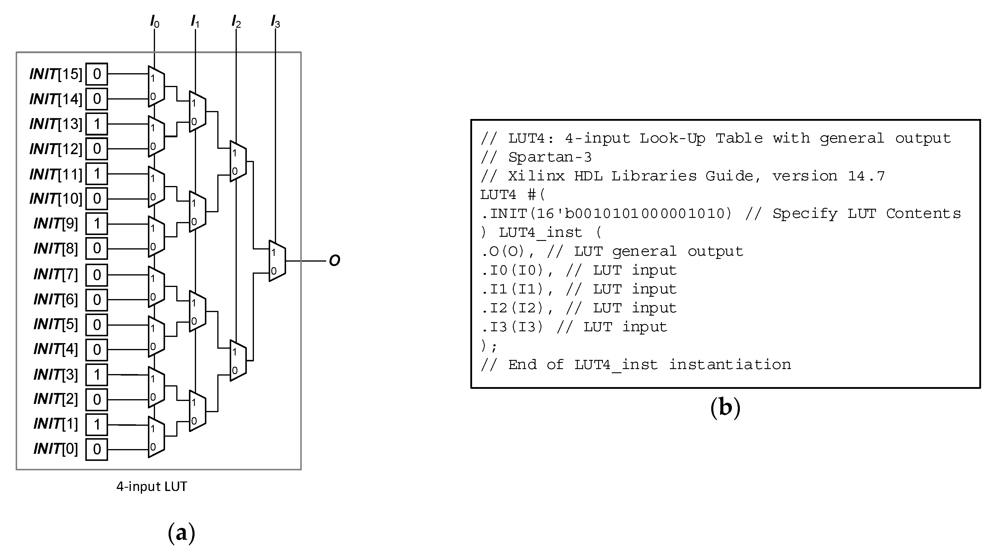
In general, FPGA employs LUTs as a primary resource to realize a target logic function. A typical N-input LUT consists of 2N 1-bit SRAM cells and N – 1 2-to-1 MUXs. Figure 2a depicts 4-input LUT as an example with 16 1-bit SRAM cells and 15 2-to-1 MUXs. Based on the structure of 4-input LUT, INIT[I] associated with the MUX input I = 4’bI3I2I1I0 is selectively determined as the output O. For instance, when the input I sets to 4’b0110 in Figure 2a, the output becomes 1 corresponding to INIT [6]. The vector form of the input is also represented as the Boolean product form by setting each i-th Boolean variable as either I i or I i ¯ depending on whether the i-th bit pattern is 1 or 0, respectively. The input I = 4’b0110 can be represented as I 3 ¯ I 2 I 1 I 0 ¯ additionally.
Using Boolean product form, we can determine all bits in INIT for a specific logic function. Let us assume that the logic function is O = I 3 I 1 ¯ I 0 + I 2 ¯ I 0 . First, the Boolean function should be expanded as the standard form that includes each input variable in all the product terms. The standard form is easily obtained by applying well-known distribution rule, I i I j + I i I k = I i ( I j + I k ) and complement rule I i + I i ¯ = 1 . The standard form of the target logic function O is computed as
O = I 3 I 1 ¯ I 0 + I 2 ¯ I 0 = I 3 ( I 2 + I 2 ¯ ) I 1 ¯ I 0 + ( I 3 + I 3 ¯ ) I 2 ¯ ( I 1 + I 1 ¯ ) I 0 = I 3 I 2 I 1 ¯ I 0 + I 3 I 2 ¯ I 1 ¯ I 0 + I 3 I 2 ¯ I 1 I 0 + I 3 I 2 ¯ I 1 ¯ I 0 + I 3 ¯ I 2 ¯ I 1 I 0 + I 3 ¯ I 2 ¯ I 1 ¯ I 0 = I 3 I 2 I 1 ¯ I 0 + I 3 I 2 ¯ I 1 I 0 + I 3 I 2 ¯ I 1 ¯ I 0 + I 3 ¯ I 2 ¯ I 1 I 0 + I 3 ¯ I 2 ¯ I 1 ¯ I 0
Based on the relation between the vector and Boolean forms, the content of LUT can be obtained as 16’b0010_1010_0000_1010. As a result, any Boolean logic function with 4 input variables can be configured in a 4-input LUT by storing suitable values in the SRAM.
Furthermore, Xilinx provides primitive libraries [30,31] of LUTs written in hardware description language (HDL) to help RTL designs to instantiate LUT. Figure 2b depicts the primitive library of 4-input LUT with the name of LUT4, the inputs of I3, I2, I1, I0, the output of O, and the initial value of 16-bit INIT. The LUT contents computed from the target logic function is initialized as a 16-bit INIT parameter. When INIT is initialized as 16’b0010_1010_0000_1010, the 4-input LUT operates the logic function O = I 3 I 1 ¯ I 0 + I 2 ¯ I 0 .
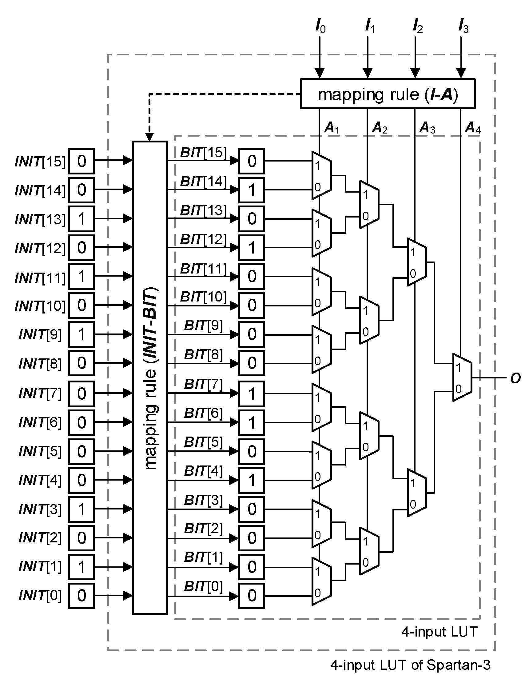
Reverse engineering seems straightforward if the LUT content identical to the INIT value is explicitly shown in the extracted bitstream since it can be easily converted using the relation between logic function and bit patterns, as described previously. However, the LUT content is not explicitly shown in the extracted bitstream unfortunately. In fact, many FPGA manufacturers, including Xilinx [32] and Intel [33], obfuscate the LUT content to protect its original design from IP theft and prevent malicious manipulation. The 4-input LUT is actually represented as Figure 3 in Xilinx Spartan-3 rather than Figure 2a. When an RTL designer instantiates a LUT with INIT bits targeting a specific logic function, the RTL designer is interested in 16-bits of INIT associated with the input variables of I0, I1, I2, and I3. However, INIT are not directly used to fabricate the commercial FPGA chips, which means that INIT[i] is not explicitly shown in the actual bitstream. Instead of 16-bits of INIT and input variables of I0, I1, I2, and I3, alternative signals denoted as 16-bits of BIT and input variables of A1, A2, A3, and A4 are internally used to provide secure operation. As shown in Figure 3, 16-bit INIT is translated as 16-bit BIT rather than using 16-bit INIT directly in bitstream. Moreover, the input variables of I0, I1, I2, and I3 are translated as A1, A2, A3, and A4, used in synthesis and implementation process in Xilinx design suits. Note that we follow the index of Aj for 1 ≤ jN as used in Xilinx design suits without loss of generality. As a result, the reverse engineering seeks to disclose the mapping rule between INIT and BIT vectors. Since a bitstream includes all BIT vectors corresponding to all LUTs in a target FPGA, reverse engineering can be successful by translating each bit BIT vector to INIT vector and converting a logic function from the translated INIT vector when a mapping rule for each LUT is completely recovered.

2.2. The Previous LUT Extract Method

Since a bitstream can be easily extracted while transferring from an external memory to FPGA by using a measurement equipment like a logic analyzer, we assume that the bitstream extraction is successfully accomplished, and thus focus on the discovery of the mapping rule. Swierczynski in [6] proposed the method to discover the mapping rule between INIT and BIT for the first time. The previous exhaustive processing [6] mainly demands three steps as follows.

2.2.1. Bit Position Search

The bit position for a target N-input LUT is searched since there is no information about the bitstream. To find the position of bits associated with the target LUT, one target N-input LUT is instantiated two times with INIT vectors of 2N-bit all zeros and ones using primitive libraries in Figure 2b. Note that the other hardware resource, except for the INIT vectors, maintain the same. From the comparison after synthesizing two designs using Xilinx ISE Design Suite, it is found that the two generated bitstreams are exactly different by 2N bits equal to the length of INIT. As an example, 16 different positions are obtained for 4-input LUT by implementing the INIT with 16-bit zeros and ones.

2.2.2. Mapping Table Construction

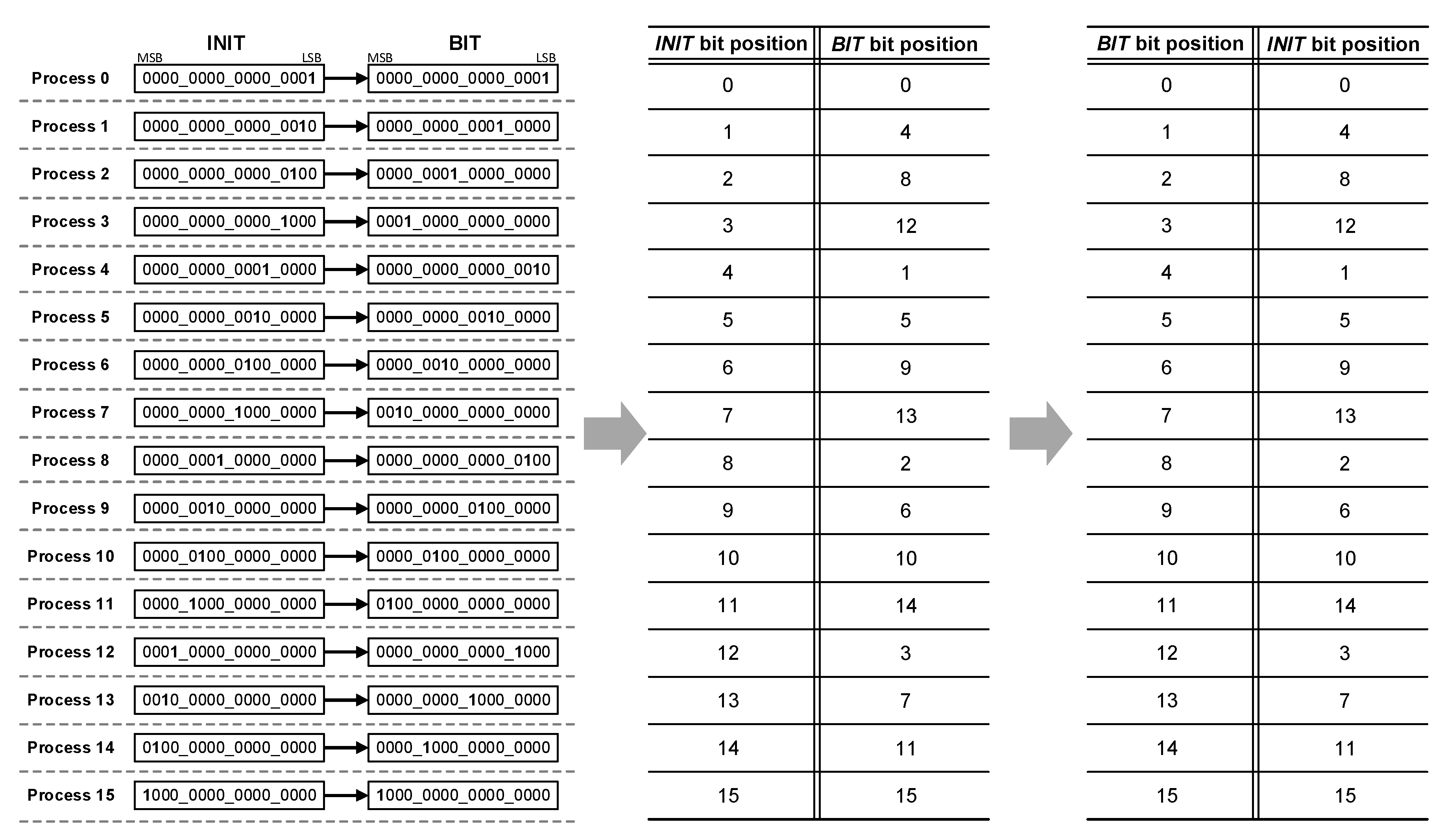
The same N-input LUT is instantiated 2N times with different INIT vectors maintaining the other hardware resources the same. For the i-th instantiation, the LUT is initialized with the INIT vector with single one on the i-th position and all zeros on the other positions. After synthesizing and implementing the target LUT, Xilinx ISE Design Suite generates a bitstream and the N-bit pattern denoted as BIT is extracted from the previously selected bit positions. The exhaustive 2N instantiation results in 2N INIT and 2N BIT vectors for the target LUT. Given 2N pairs of INIT and BIT vectors, the mapping table is finally constructed by extracting the position of single one from the pairs of vectors. Figure 4 exemplifies the construction of the mapping table for 4-input LUT. For instance, when INIT sets to 16’b0000_0000_1000_0000, BIT becomes 16’b0010_0000_0000_0000 through Xilinx synthesis and an implementation process, and the relation between INIT [7] and BIT [13] is obtained. From the exhaustive 16 processing, all elements in the mapping table can be completely filled.
Lastly, it is noticeable that BIT for all Xilinx FPGAs does not always has single one vector although the INIT is initialized with single one vector. As an example, BIT for Xilinx Spartan-3 is single zero vector whereas BIT for Xilinx Virtex-5 is single one vector. For instance, INIT 16’b0000_0000_1000_0000 in Xilinx Spartan-3 results in BIT 16’b1101_1111_1111_1111 instead of 16’b0010_0000_0000_0000. As BIT is either single one or zero vector, the mapping table can be seamlessly constructed if BIT inversion checks once.

2.2.3. Logic Restoration

After constructing the mapping table, the final step to restore a logic function is straightforward. First, the 2N bit vector denoted as BIT is extracted from the bitstream based on the selected bit positions of Section 2.2.1. The constructed mapping table of Section 2.2.2 allows to convert a 2N BIT vector to a 2N INIT vector. Since INIT vector is the content of the LUT, INIT vector is translated as the LUT inputs of I0, I1, I2, and I3 according to Boolean representation. As an example, assume that the target BIT is 16’b0101_0000_1101_0000 extracted from the target bitstream at the selected bit position of bit position search in Section 2.2.1. Once BIT vector is acquired, INIT is simply obtained as 16’b0010_1010_0000_1010 by rearranging BIT based on the mapping table shown in Figure 4. Using the Boolean representation, INIT [1], INIT [3], INIT [9], INIT [11] and INIT [13] in INIT vector are converted as I 3 ¯ I 2 ¯ I 1 ¯ I 0 , I 3 ¯ I 2 ¯ I 1 I 0 , I 3 I 2 ¯ I 1 ¯ I 0 , I 3 I 2 ¯ I 1 I 0 and I 3 I 2 I 1 ¯ I 0 . Finally, the logic function O = I 3 I 2 I 1 ¯ I 0 + I 3 I 2 ¯ I 1 I 0 + I 3 I 2 ¯ I 1 ¯ I 0 + I 3 ¯ I 2 ¯ I 1 I 0 + I 3 ¯ I 2 ¯ I 1 ¯ I 0 is restored from BIT 16’b 0101_0000_1101_0000.
The previous method with 2N exhaustive processing has succeeded in restoring a logic function of a LUT from the bitstream. However, it is impractical in that a FPGA generally contains more than hundreds and thousands of LUTs, and thus the number of processing increases exponentially when the previous exhaustive method [6] is applied. Therefore, it is necessary to improve the previous method to provide a practical reverse engineering solution for LUTs.

3. Proposed Method

In this paper, we present a new fast method to reduce recovery time by saving the number of processing. Whereas the previous exhaustive method [6] to perform reverse engineering on an N-input LUT requires 2N processing exponential to N to perform reverse engineering on an N-input LUT, the proposed method requires 2N processing linear to N. The main idea of the proposed method is to employ an individual basis of Ii (0 ≤ i < N), not the entire vector form of I = IN-1IN-2I1I0. For the case of 4-input LUT, as an example, the previous exhaustive method [6] generates 16 BIT vectors from all possible INIT vectors from I = 0, i.e., I3I2I1I0 = 0000, to I = 15, i.e., I3I2I1I0 = 1111. However, the proposed method generates 4 BIT vectors according to individual input I0, I1, I2, and I3, and the 4 BIT vectors are used as a basis to construct a mapping table.
The generation of 2N-bit BIT vectors for individual input Ii (0 ≤ i < N) seems straightforward. The individual input Ii (0 ≤ i < N) seems possible to be synthesized and implemented using N-input LUT primitive library initialized with an appropriate 2N-bit INIT vector, as the vector form of I = IN-1IN-2I1I0 is instantiated in the previous method. The INIT vector can be computed using Boolean distribution and complement rules. For instance, INIT value of I0 is 16’b1010_1010_1010_1010 since
I 0 = I 0 ( I 1 + I 1 ¯ ) ( I 2 + I 2 ¯ ) ( I 3 + I 3 ¯ ) = I 3 I 2 I 1 I 0 + I 3 I 2 I 1 ¯ I 0 + I 3 I 2 ¯ I 1 I 0 + I 3 I 2 ¯ I 1 ¯ I 0 + I 3 ¯ I 2 I 1 I 0 + I 3 ¯ I 2 I 1 ¯ I 0 + I 3 ¯ I 2 ¯ I 1 I 0 + I 3 ¯ I 2 ¯ I 1 ¯ I 0
This attempt to use the LUT primitive library with a single input seems logical, but it is actually impossible to generate a BIT vector due to practical reasons. While synthesizing and optimizing the LUT, the Xilinx ISE Design Suite generally eliminates the LUT instantiated with a single input. Instead of the LUT instantiation, the single input is directly bypassed to the output to save hardware resource. Note that as far as we know, there is no feasible way to synthesize and implement an LUT primitive library with a single input using Xilinx ISE Design Suite.

3.1. I-A Mapping Construction

To solve this problem, the proposed method employs Xilinx Design Language (XDL) [34,35], which describes the utilized hardware components for the current target design among the entire hardware resources in FPGA. In Xilinx ISE Design Suite, XDL [34,35] is generated automatically to provide the RTL designers for verifying the target design’s synthesis and optimization. Figure 5 shows the example of XDL [34,35] captured from Xilinx Spartan-3. The red box in XDL [34,35] indicates that the current design instantiates LUT4 whose internal Boolean function is (A3((~A4 * A2) + ~A1)) when synthesizing a 4-input LUT with target function I 3 I 1 ¯ I 0 + I 2 ¯ I 0 . As previously descried in Section 2, the actual configuration of LUT in Figure 3 is not the same as the ideal LUT in Figure 2a.
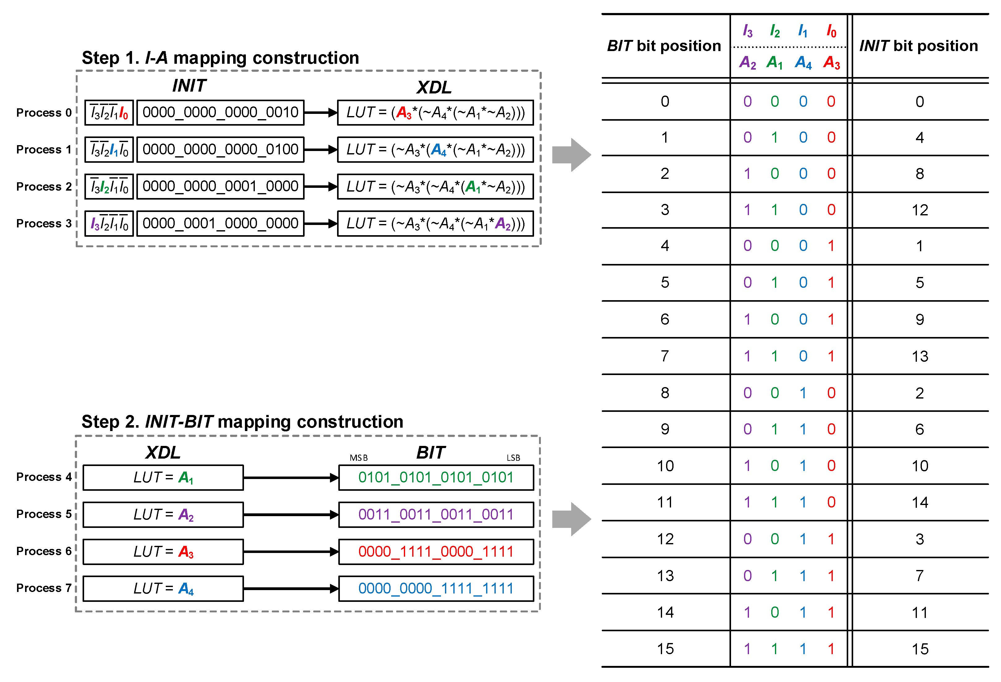
Since an LUT cannot be implemented with a single input Ii (0 ≤ i < N) due to practical reasons, the proposed method instantiates a specific form of I = IN-1IN-2I1I0 that can distinguish the relation between input variable Ii (0 ≤ i < N) and internal variable Aj(1 ≤ jN). More precisely, I sets to the combination of single I i and other I i ¯ . For instance, 4-input LUT is instantiated with I 3 ¯ I 2 ¯ I 1 ¯ I 0 , I 3 ¯ I 2 ¯ I 1 I 0 ¯ , I 3 ¯ I 2 I 1 ¯ I 0 ¯ and I 3 I 2 ¯ I 1 ¯ I 0 ¯ . Using this specific form of I and corresponding XDL [34,35], a feasible solution is provided to map input variable Ii (0 ≤ i < N) and internal variable Aj(1 ≤ jN). As an example, Figure 6 shows that input I of I 3 ¯ I 2 ¯ I 1 ¯ I 0 , I 3 ¯ I 2 ¯ I 1 I 0 ¯ , I 3 ¯ I 2 I 1 ¯ I 0 ¯ and I 3 I 2 ¯ I 1 ¯ I 0 ¯ are initialized in the target LUT with a different 16-bit INIT vector, resulting in different XDLs. Based on the input I and XDL [34,35] described in Figure 6, pairs of (I0, A3), (I1, A4), (I2, A1), and (I3, A2) are recovered. Thus, N-input LUT demands N processing to completely build the IA mapping table.

3.2. INIT-BIT Mapping Construction

To recover programmable points such as PLP and PIP, many previous researches [14,15,16,17,18,19,20,21] employ XDL [34,35] to modify the original design as intended. In the proposed method, XDL [34,35] is modified to instantiate an LUT with a single internal variable Aj (1 ≤ jN). Since synthesis with a single input Ii(0 ≤ i < N) is practically infeasible, we synthesize LUTs with a single internal variable Aj (1 ≤ jN) alternatively. Using the mapping relation between IiAj obtained at the previous step, the generated BIT associated with an internal variable Aj (1 ≤ jN) is rearranged to restore a mapping table. Figure 6 depicts the overall process for the proposed fast reverse engineering method. For a 4-input LUT, each LUT is instantiated with an individual internal variable Aj (1 ≤ jN) by modifying XDL [34,35], and 16-bit BIT for each individual internal variable Aj (1 ≤ jN) is generated. Since the pairs of (I0, A3), (I1, A4), (I2, A1), (I3, A2) are discovered, 4 BIT vectors associated with Aj (1 ≤ jN) are allocated at the mapping table in the order of A2, A1, A4, and A3. Consequently, Figure 6 shows the mapping table computed from the proposed fast method. Note that it is identical to the mapping table computed from the previous exhaustive method in Figure 4. Since the same mapping table is obtained in both previous and proposed methods, the same results are guaranteed. To sum up, we tried to obtain 16-bit BIT associated with each input variable Ii (0 ≤ i < N) to reduce processing complexity from exponential increase to linear increase at the first time. However, the practical issue prohibits from instantiating an LUT with a single variable Ii (0 ≤ i < N), so we implement a LUT with a single internal variable Aj (1 ≤ jN) using the help of XDL. First, an IA mapping table is constructed, and BIT vectors corresponding to the internal variable Aj (1 ≤ jN) are generated. Lastly, the INIT-BIT mapping table is constructed using I-A relation and BIT vectors. The proposed method requires N processing to build a mapping table between Ii (0 ≤ i < N) and Aj (1 ≤ jN) and additional N processing for building BIT vectors associated with Aj (1 ≤ jN).

4. Experimental Results

Since the final mapping tables between INIT-BIT are the same as shown in Figure 4 and Figure 6, the previous and proposed methods always provide the same reverse outputs. To compare two methods in terms of recovery time, we measure the total processing time to restore a target function from a bitstream. The previous and proposed methods can be applied to all Xilinx FPGAs, which are synthesized and implemented with Xilinx ISE Design Suite. As an example, low-end FPGA of Xilinx Spartan-3 equipped with 4-input LUTs and high-end FPGA of Xilinx Virtex-5 equipped with 6-input LUTs are synthesized, and Xilinx ISE Design Suite v10.1 is used to generated BIT vectors under 3.7 GHz Intel Core i5 with 16 G RAM in the experiments. Table 1 shows the details of recovery time for a single LUT restoration. Both methods consist of three steps: bit position search, mapping table construction, and logic restoration, and the proposed method uses the same bit position search and logic restoration but improves mapping table construction compared with the previous method. As described in the previous sections, the proposed method saves the processing from 2N to 2N and results in significant improvement in mapping table construction. In addition, mapping table construction contains the majority of recovery time, and therefore the overall reduction from the proposed method is significant for both Xilinx Sparatn-3 and Virtex-5. According to Table 1, the proposed method saves recovery time by 57% and 86% for Xilinx Spartan-3 and Virtex-5, respectively.
For a practical comparison, various benchmarks and real cryptography applications are implemented in Xilinx Spartan-3 and Virtex-5. Table 2 shows the number of utilized LUTs and total recovery time according to reverse engineering methods. Five designs from ISCAS’85 benchmarks are implemented, whose LUTs ranges from 2 to 703. As practical application, data encryption standard (DES) and advanced encryption standard (AES) are implemented, whose LUTs ranges from 983 to 7644. It is noticeable that the number of the utilized LUTs differs depending on Xilinx FPGA due to the fact that a different FPGA includes difference internal hardware resources. For example, when the DES circuit is synthesized and implemented, Xilinx Spartan-3 requires 1397 4-input LUTs and Xilinx Virtex-5 requires 983 6-input LUT LUTs. Significant improvement is expected in Table 2, since the total recovery time is proportional to the unit recovery time for a single LUT. According to Table 2, the proposed method shows superior recovery time through all comparisons, given the bitstream generated from the identical design. For instance, when the DES circuit is recovered, the proposed method saves 57% in Xilinx Spartan-3 equipped with 4-input LUT and 85% in Xilinx Virtex-5 equipped with 6-input LUT compared to the previous exhaustive method. It is noticeable that the reduction time becomes more significant as the number of input increases.

5. Conclusions

This paper presents a novel logic extraction method from Xilinx FPGA bitstreams. Whereas the previous method demands exhaustive 2N processing for a N-input LUT, the proposed method reduces the processing to 2N. In experimental results, Xilinx Spartan-3 equipped with 4-input LUTs and Virtex-5 equipped with 6-input LUTs are utilized for a fair comparison. Various designs associated with ISCAS’85 benchmarks and cryptography applications are implemented, and all the results show that the proposed method outperforms the previous method. According to the experimental results, the proposed method can save 57% and 86% recovery time compared to the previous method. The improvement becomes more significant in future Xilinx FPGAs as the commercial Xilinx FPGAs tend to include LUTs with more inputs. Our next research aim is to study a fast reversing method for high-end FPGA chips using Xilinx Vivado that uses more complex obfuscation compared to Xilinx ISE Design Suite.

Author Contributions

Conceptualization, H.Y.; methodology, S.C.; software, S.C.; validation, S.C. and H.Y.; formal analysis, H.Y.; investigation, S.C.; resources, S.C.; data curation, S.C.; writing—original draft preparation, S.C.; writing—review and editing, H.Y.; visualization, S.C.; supervision, H.Y.; project administration, H.Y.; funding acquisition, H.Y. All authors have read and agreed to the published version of the manuscript.

Funding

This research funded by research fund of Chungnam National University.

Acknowledgments

This work was supported by research fund of Chungnam National University.

Conflicts of Interest

The authors declare no conflict of interest.

References

  1. Yu, H.; Lee, H.; Lee, S.; Kim, Y.; Lee, H.-M. Recent Advances in FPGA Reverse Engineering. Electronics 2018, 7, 246. [Google Scholar] [CrossRef] [Green Version]
  2. Lysaght, P.; Blodget, B.; Mason, J.; Young, J.; Bridgford, B. Invited Paper: Enhanced Architectures, Design Methodologies and CAD Tools for Dynamic Reconfiguration of Xilinx FPGAs. In Proceedings of the 2006 International Conference on Field Programmable Logic and Applications, Madrid, Spain, 28–30 August 2006. [Google Scholar]
  3. Yokoyama, H.; Toda, K. FPGA-based content protection system for embedded consumer electronics. In Proceedings of the 11th IEEE International Conference on Embedded and Real-Time Computing Systems and Applications (RTCSA’05), Hong Kong, China, 17–19 August 2005. [Google Scholar]
  4. Chamola, V.; Patra, S.; Kumar, N.; Guizani, M. FPGA for 5G: Re-configurable Hardware for Next Generation Communication. IEEE Wirel. Commun. 2020, 27, 140–147. [Google Scholar] [CrossRef]
  5. Cao, T.P.; Deng, G.; Mulligan, D. Implementation of real-time pedestrian detection on FPGA. In Proceedings of the 23rd International Conference Image and Vision Computing New Zealand, Christchurch, New Zealand, 26–28 November 2008. [Google Scholar]
  6. Swierczynski, P.; Fyrbiak, M.; Koppe, P.; Paar, C. FPGA Trojans Through Detecting and Weakening of Cryptographic Primitives. IEEE Trans. Comput. Aided Des. Integr. Circuits Syst. 2015, 34, 1236–1249. [Google Scholar] [CrossRef]
  7. Greene, J.; Hamdy, E.; Beal, S. Antifuse field programmable gate arrays. Proc. IEEE 1993, 81, 1042–1056. [Google Scholar] [CrossRef]
  8. McCollum, J. ASIC versus antifuse FPGA reliability. In Proceedings of the 2009 IEEE Aerospace conference, Big Sky, MT, USA, 7–14 March 2009. [Google Scholar]
  9. M. Kamoun, N.; Bossuet, L.; Ghazel, A. Experimental implementation of 2ODPA attacks on AES design with flash-based FPGA technology. In Proceedings of the 2010 International Conference on Microelectronics, Cairo, Egypt, 19–22 December 2010. [Google Scholar]
  10. Greene, J.; Kaptanoglu, S.; Feng, W.; Hecht, V.; Landry, J.; Li, F.; Krouglyanskiy, A.; Morosan, M.; Pevzner, V. A 65nm flash-based FPGA fabric optimized for low cost and power. In Proceedings of the 19th ACM/SIGDA international symposium on Field programmable gate arrays (FPGA ’11), Monterey, CA, USA, 27 February–1 March 2011. [Google Scholar]
  11. Heron, O.; Arnaout, T.; Wunderlich, H. On the reliability evaluation of SRAM-based FPGA designs. In Proceedings of the International Conference on Field Programmable Logic and Applications, Tampere, Finland, 24–26 August 2005. [Google Scholar]
  12. Wirthlin, M. High-reliability FPGA-based systems: Space, high-energy physics, and beyond. Proc. IEEE 2015, 103, 379–389. [Google Scholar] [CrossRef]
  13. Gören, S.; Ozkurt, O.; Yildiz, A.; Ugurdag, H.F. FPGA bitstream protection with PUFs, obfuscation, and multi-boot. In Proceedings of the 6th International Workshop on Reconfigurable Communication-Centric Systems-on-Chip (ReCoSoC), Montpellier, France, 20–22 June 2011. [Google Scholar]
  14. Note, J.-B.; Rannaud, É. From the bitstream to the netlist. In Proceedings of the 16th international ACM/SIGDA symposium on Field programmable gate arrays, New York, NY, USA, 24–26 February 2008. [Google Scholar]
  15. Benz, F.; Seffrin, A.; Huss, S.A. Bil: A tool-chain for bitstream reverse-engineering. In Proceedings of the 22nd International Conference on Field Programmable Logic and Applications (FPL), Oslo, Norway, 29–31 August 2012. [Google Scholar]
  16. Ding, Z.; Wu, Q.; Zhang, Y.; Zhu, L. Deriving an NCD file from an FPGA bitstream: Methodology, architecture and evaluation. Microprocess. Microsyst. 2013, 37, 299–312. [Google Scholar] [CrossRef]
  17. Yoon, J.; Seo, Y.; Jang, J.; Cho, M.; Kim, J.; Kim, H.; Kwon, T. A Bitstream Reverse Engineering Tool for FPGA Hardware Trojan Detection. In Proceedings of the 2018 ACM SIGSAC Conference on Computer and Communications Security, Toronto, ON, Canada, 15–19 October 2018. [Google Scholar]
  18. Seo, Y.; Yoon, J.; Jang, J.; Cho, M.; Kim, H.; Kwon, T. Poster: Towards reverse engineering FPGA bitstreams for hardware trojan detection. In Proceedings of the Network Distribution System Security Symposium (NDSS), San Diego, CA, USA, 18–21 February 2018. [Google Scholar]
  19. Zhang, T.; Wang, J.; Guo, S.; Chen, Z. A Comprehensive FPGA Reverse Engineering Tool-Chain: From Bitstream to RTL Code. IEEE Access 2019, 7, 38379–38389. [Google Scholar] [CrossRef]
  20. Ender, M.; Swierczynski, P.; Wallat, S.; Wilhelm, M.; Knopp, P.M.; Paar, C. Insights into the mind of a trojan designer. In Proceedings of the 24th Asia and South Pacific Design Automation Conference, Tokyo, Japan, 21–24 January 2019. [Google Scholar]
  21. Choi, S.; Park, J.; Yoo, H. Reverse Engineering for Xilinx FPGA Chips using ISE Design Tools. J. Integr. Circuits Syst. 2020, 6, 1. [Google Scholar]
  22. Project X-Ray. Available online: https://symbiflow.readthedocs.io/projects/prjxray/en/latest/ (accessed on 12 June 2020).
  23. Yu, H.; Lee, H.; Shin, Y.; Kim, Y. FPGA reverse engineering in Vivado design suite based on X-ray project. In Proceedings of the 2019 International SoC Design Conference (ISOCC), Jeju, Korea, 6–9 October 2019. [Google Scholar]
  24. Chakraborty, R.S.; Narasimhan, S.; Bhunia, S. Hardware Trojan: Threats and emerging solutions. In Proceedings of the 2009 IEEE International High Level Design Validation and Test Workshop, San Francisco, CA, USA, 4–6 November 2009. [Google Scholar]
  25. Wallat, S.; Fyrbiak, M.; Schlögel, M.; Paar, C. A Look at the Dark Side of Hardware Reverse Engineering—A Case Study. In Proceedings of the 2017 IEEE 2nd International Verification and Security Workshop (IVSW), Thessaloniki, Greece, 3–5 July 2017. [Google Scholar]
  26. Chakraborty, R.S.; Saha, I.; Palchaudhuri, A.; Naik, G.K. Hardware Trojan Insertion by Direct Modification of FPGA Configuration Bitstream. IEEE Des. Test 2013, 30, 45–54. [Google Scholar] [CrossRef]
  27. Khaleghi, B.; Ahari, A.; Asadi, H.; Bayat-Sarmadi, S. FPGA-Based Protection Scheme against Hardware Trojan Horse Insertion Using Dummy Logic. IEEE Embedded Sys. Lett. 2015, 7, 46–50. [Google Scholar] [CrossRef]
  28. Swierczynski, P.; Fyrbiak, M.; Paar, C.; Huriaux, C.; Tessier, R. Protecting against Cryptographic Trojans in FPGAs. In Proceedings of the 2015 IEEE 23rd Annual International Symposium on Field-Programmable Custom Computing Machines, Vancouver, BC, Canada, 2–6 May 2015. [Google Scholar]
  29. Jeong, M.; Lee, J.; Jung, E.; Kim, Y.H.; Cho, K. Extract LUT Logics from a Downloaded Bitstream Data in FPGA. In Proceedings of the 2018 IEEE International Symposium on Circuits and Systems (ISCAS), Florence, Italy, 27–30 May 2018. [Google Scholar]
  30. Xilinx. Spartan-3 Libraries Guide for HDL Designs; Xilinx: San Jose, CA, USA, 2013. [Google Scholar]
  31. Xilinx. Virtex-5 Ligraries Guide for HDL Designs; Xilinx: San Jose, CA, USA, 2013. [Google Scholar]
  32. Xilinx. Available online: http://www.xilinx.com (accessed on 12 June 2020).
  33. Intel FPGA. Available online: https://www.intel.com/content/www/us/en/products/programmable/fpga.html?elq_cid=4776342&erpm_id=7614038 (accessed on 12 June 2020).
  34. Beckhoff, C.; Koch, D.; Torresen, J. The Xilinx Design Language (XDL): Tutorial and use cases. In Proceedings of the 6th International Workshop on Reconfigurable Communication-Centric Systems-on-Chip (ReCoSoC), Montpellier, France, 20–22 June 2011. [Google Scholar]
  35. Lavin, C.; Padilla, M.; Lamprecht, J.; Lundrigan, P.; Nelson, B.; Hutchings, B. RapidSmith: Do-It-Yourself CAD Tools for Xilinx FPGAs. In Proceedings of the 2011 21st International Conference on Field Programmable Logic and Applications, Chania, Greece, 5–7 September 2011. [Google Scholar]
Figure 1. Typical FPGA structure.
Electronics 09 01132 g001
Figure 2. (a) Structure and (b) primitive library for 4-input LUT.
Electronics 09 01132 g002
Figure 3. Actual 4-iput LUT structure in Xilinx Spartan-3.
Electronics 09 01132 g003
Figure 4. Mapping table construction for the previous method [6].
Electronics 09 01132 g004
Figure 5. Example of XDL in Spartan-3.
Electronics 09 01132 g005
Figure 6. Mapping table construction for the proposed method.
Electronics 09 01132 g006
Table 1. Comparison of recovery time for a single LUT.
FPGA type (LUT type)Spartan-3 (4-input LUT)Virtex-5 (6-input LUT)
AlgorithmExhaustive [6]ProposedExhaustive [6]Proposed
Bit position search1.1 min1.1 min (0%)1.6 min1.6 min (0%)
Mapping table construction8.5 min3.1 min (64%)52 min6.3 min (88%)
Logic restoration0.01 ms0.01 ms (0%)5 ms5 ms (0%)
Total time9.6 min4.1 min (57%)53.6 min7.9 min (86%)
Table 2. Comparison of recovery time for ISCAS’85 benchmarks and practical applications.
FPGA (LUT Type)Spartan-3 (4-input LUT)Virtex-5 (6-input LUT)
Algorithm# of LUTTime# of LUTTime
Exhaustive [6]ProposedExhaustive [6]Proposed
ISCAS’85 BenchmarkC17219.2 min8.3 min21.8 h15.9 min
C4997813.1 h5.7 h662.5 days8.7 h
C88011518.6 h8.0 h772.9 days10.2 h
C190810316.2 h6.9 h813.0 days10.7 h
C35403262.2 days0.9 days2228.3 days1.2 days
C62887034.7 days2.0 days4682.5 weeks2.6 days
Practical applicationsDES13979.3 days4.0 days9835.2 weeks5.4 days
AES76447.3 weeks3.1 weeks274214.7 weeks2.2 weeks