Article

Design and Implementation of a Compact Single-Photon Counting Module

1
Guangxi Key Laboratory of Optoelectronic Information Processing, School of Electronic Engineering and Automation, Guilin University of Electronics Technology, Guilin 541004, China
2
School of Information and Communication, Guilin University of Electronics Technology, Guilin 541004, China
3
Department of Electrical and Electronic Engineering, University College Cork, Cork T12 K8AF, Ireland
*
Authors to whom correspondence should be addressed.
Electronics 2020, 9(7), 1131; https://doi.org/10.3390/electronics9071131
Submission received: 2 June 2020 / Revised: 3 July 2020 / Accepted: 9 July 2020 / Published: 11 July 2020
(This article belongs to the Section Microelectronics)

Abstract

:
A compact single-photon counting module that can accurately control the bias voltage and hold-off time is developed in this work. The module is a microcontroller-based system which mainly consists of a microcontroller, a programmable negative voltage generator, a silicon-based single-photon avalanche diode, and an integrated active quench and reset circuit. The module is 3.8 cm × 3.6 cm × 2 cm in size and can communicate with the end user and be powered through a USB cable (5 V). In this module, the bias voltage of the single-photon avalanche diode (SPAD) is precisely controllable from −14 V ~ −38 V and the hold-off time (consequently the dead time) of the SPAD can be adjusted from a few nanoseconds to around 1.6 μs with a setting resolution of ∼6.5 ns. Experimental results show that the module achieves a minimum dead time of around 28.5 ns, giving a saturation counting rate of around 35 Mcounts/s. Results also show that at a controlled reverse bias voltage of 26.8 V, the dark count rate measured is about 300 counts/s and the timing jitter measured is about 158 ps. Photodetection probability measurements show that the module is suited for detection of visible light from 450 nm to 800 nm with a 40% peak photon detection efficiency achieved at around 600 nm.

1. Introduction

Single-photon counting techniques have been used in low-light sensing applications such as LIDAR [1,2], quantum key distribution [3], medical imaging technology [4], and 3D imaging technology [5,6]. Photomultiplier tubes have been the traditional solution for photon counting applications, but in recent years single-photon avalanche diode (SPAD) has become an alternative candidate due to its lower cost, lower operating voltage, higher sensitivity, and smaller size.
The dead time in a SPAD is the off time when the SPAD is quenched after every avalanche event to dissipate trapped charge, thereby minimizing the “afterpulsing” phenomenon. As a result, a trade-off exists between the maximum photon counting rate and an acceptable level of noise. An accurate adjustment of the dead time is important to achieve an optimal dead time (and consequently optimal maximum photon counting rate) in a single-photon counting system. The bias voltage has a major effect on the SPAD’s important performance parameters such as dark count rate (DCR) and photon detection efficiency (PDE). A higher bias voltage will lead to better PDE due to the increase in the avalanche trigger probability. However, the potential drawbacks include higher DCR and the considerable afterpulsing effect. Therefore, the bias voltage should be adjustable and optimized to achieve best overall performance. Several SPAD-based single-photon counting modules have been developed [7,8,9,10,11,12,13,14,15,16,17] but these modules are limited in that the dead time and bias voltage of the detector are difficult to change. This limits their usefulness in varying environments and for the case where the detector needs to be changed for different measurement purposes. In addition, existing designs are usually bulky and cumbersome, which limits their usefulness in applications that require compact solutions.
In this work, a compact multi-parameter adjustable single-photon counting module is developed. The module is a microcontroller-based system mainly consisting of a programmable negative voltage generator, a silicon-based SPAD, an active quenching and reset integrated circuit (AQR-IC) and I/O components. In this module, a custom designed SPAD was fabricated and used with its bias voltage precisely controllable from −14 V ~ −38 V using a programmable negative voltage generator. With the AQR-IC, the hold-off time (consequently the dead time) in the SPAD can be adjusted from a few nanoseconds to around 1.6 µs with a setting resolution of ∼6.5 ns. A microcontroller of the module is used to drive and control the SPAD’s bias voltage and hold-off time which can also be connected to a PC through USB for the graphical user interface. With the control of the bias voltage and high-resolution setting of the dead time, intelligent control can be added to the module for detection optimizations under varying environments that greatly improve the SPAD-based photon counting system’s robustness. In addition, the module developed is about 3.8 cm × 3.6 cm × 2 cm in volume, allowing it to be used in compact photon counting systems. Experimental results show that the module achieves a minimum dead time of around 28.5 ns which demonstrates a saturation counting rate of around 35 Mcounts/s. At a controlled reverse bias voltage of 26.8 V, the DCR measured is about 300 counts/s and the timing jitter measured is about 158 ps. Photodetection probability measurements show that the module is suited for detection of visible light from 450 nm to 800 nm with a 40% peak PDE at around 600 nm.

2. System Description

Figure 1 shows the block diagram of the single-photon counting module consisting of the following parts: (1) A Microcontroller (STC89C52RC) circuitry which is used to communicate with the user end (PC) via an USB to TTL chip and also used for the control of bias voltage and the hold-off time; (2) A programmable negative voltage generator which is used to generate a stable and controllable negative high voltage for the SPAD; (3) An active quenching and reset integrated circuit (AQR-IC) for the hold-off time setting in the SPAD and (4) A custom designed SPAD.

2.1. Microcontroller Circuitry

In the microcontroller circuitry, a crystal oscillator is used to provide the clock pulses to the microcontroller chip which is powered through a USB cable. The circuitry is used to receive the control information (including hold-off time and bias voltage value) from PC (end user) through the USB-TTL converter chip and sends the control signals to related circuitry for the bias voltage and hold-off time setting in the SPAD. The microcontroller sets the eight binary ports S0~S7 of the AQR-IC, from 0 (“00000000”) to 255 (“11111111”) to achieve the hold-off time of 6.5 ns~1.6 μs in the SPAD. It also sends “ADJ” signal to the programmable negative voltage generator to achieve the required negative bias voltage for biasing the SPAD.

2.2. Programmable Negative Voltage Generator

Figure 2 shows the schematic of the programmable negative voltage generator. In the circuit, a boost circuit (consists of a bipolar transistor, an inductor, a diode and two capacitors) is used to generate high negative output voltage and a MAX749 chip (digitally adjustable bias regulator) [18]-based circuit is used to drive the boost circuit, detect the feedback signal, and maintain the output voltage at a set value. The output of the programmable negative voltage generator is determined by the internal reference current, IREF of the chip which is set by the microcontroller (through signal line, ADJ). When the voltage generator is operating, if the current flowing through the feedback resistance (RFB), IS, is greater than the reference current, IREF, the boost circuit will be stopped and the absolute value of the output voltage will drop and the IS will decrease. If IS falls below IREF, the boost circuit will be driven to continue to boost the output and the absolute value of the output voltage will increase and the IS will increase. In this way, IS can be set equal to IREF and the output voltage −VOUT can be controlled as follows:
V OUT = I REF × R FB
In this design, the feedback resistance RFB is set to 2 MΩ and the reference current can be set from around 7 μA to 19 μA. This makes the setting range of the programmable negative voltage generator to be around −14 V ~ −38 V.

2.3. SPAD and AQR-IC

The SPAD and AQR-IC used in the module are previously designed chips [19,20,21,22]. The SPAD is a 20 µm diameter planar SPAD which is based on a shallow p-n junction. It is manufactured in p-type epitaxially grown bulk silicon using a 1.5 µm complementary metal–oxide–semiconductor (CMOS) compatible process and suited for detection of visible wavelengths (from 400 nm to 850 nm) [19,20]. In the SPAD, a p-substrate with a p-type doping forming the central active area and the N+ doping overlaps the active area, forms the diode cathode, and contact to metal layers. The overlapping guard ring, and the diode forms with the p-substrate, prevents edge breakdown of the central active area. The AQR-IC is used to actively quench the SPAD after each avalanche event (lower its reverse bias voltage below its breakdown voltage), keep it in “OFF” state for a period of user-defined time (hold-off time) and set the reverse bias voltage back to its original level for the next avalanche detection. The hold-off time (and the dead time) is controlled by the end user through the PC and the microcontroller chip. With the developed active quenching and reset IC, the maximum counting rate of the module can be greatly extended and the after pulsing effects can be effectively reduced. The photos of the fabricated SPAD and AQR-IC can be seen in Figure 3a,b, respectively.

3. Experimental Results

Figure 4 shows the assembled single-photon counting module. The module consists of a main board, a cubic black package, and a fiber adapter that allows coupling of incident light to the SPAD through a fiber.
Figure 5a shows the experimental results for the reverse bias voltage setting in the module. By inputting the required voltage in the user graphic interface (GUI), the bias voltage will be adjusted. Results show that the bias voltage can be accurately set from −14 V to −38 V with standard deviation of less than 0.06 V and output voltage ripples of less than 50 mV. The setting range and resolution can be changed by setting the feedback current flowing to the feedback port of the MAX749 chip in the programmable negative voltage generator circuit. Figure 5b shows the setting of the hold-off time in SPAD of the module. The hold-off time can also be adjusted using the PC-based GUI. As can be seen from the figure, by changing the input code from “1” to “255”, the hold-off time in the SPAD can be linearly and precisely adjusted from several nano seconds to 1.6 µs with a setting resolution of about 6.5 ns. With the minimum hold-off time, a dead-time of around 28.5 ns can be achieved, giving a saturation counting rate of around 35 Mcounts/s.
To test the PDE and the dark count characteristics of the module, an experimental setup shown in Figure 6 was built. In the setup, a broad band light source (Thorlabs SLS201L/M) is used with its output light guided to a filter holder (Thorlabs FOFMF/M) by a fiber and the output of the filter holder is connected to the SPAD using another fiber. Optical band-pass filters and attenuation filters are used to alter the spectrum and power intensity of the light directed to the SPAD. A counter (FCA3100) is used to record the pulse counting rate at the output of the module.
Figure 7 shows the DCR measured for different bias voltages. This measurement was carried out when the light source is turned off and the hold-off times was set to about 100 ns, 500 ns, and 1000 ns. Results show that with overran excess bias voltage of 1 V (reverse bias voltage of around 25.6 V), the DCR in the SPAD is about 80 counts/s and when the excess bias voltage increased to 3 V, the DCR increases to about 1 kcounts/s.
Figure 8 shows the PDE measured for different wavelengths and reverse bias voltages. In the measurement, a broad-spectrum light source is used to provide the incident light to the module and optical filters are used to select the specific wavelength and alter the power intensity of the incident light. For each specific wavelength, the incident light power and the photon counting rate of the module are measured and the PDE of the module is calculated. Results show that the module is suited for detecting the short wavelengths of the incident light from 400 nm to 800 nm with a peak PDE of about 40% achieved at 600 nm.
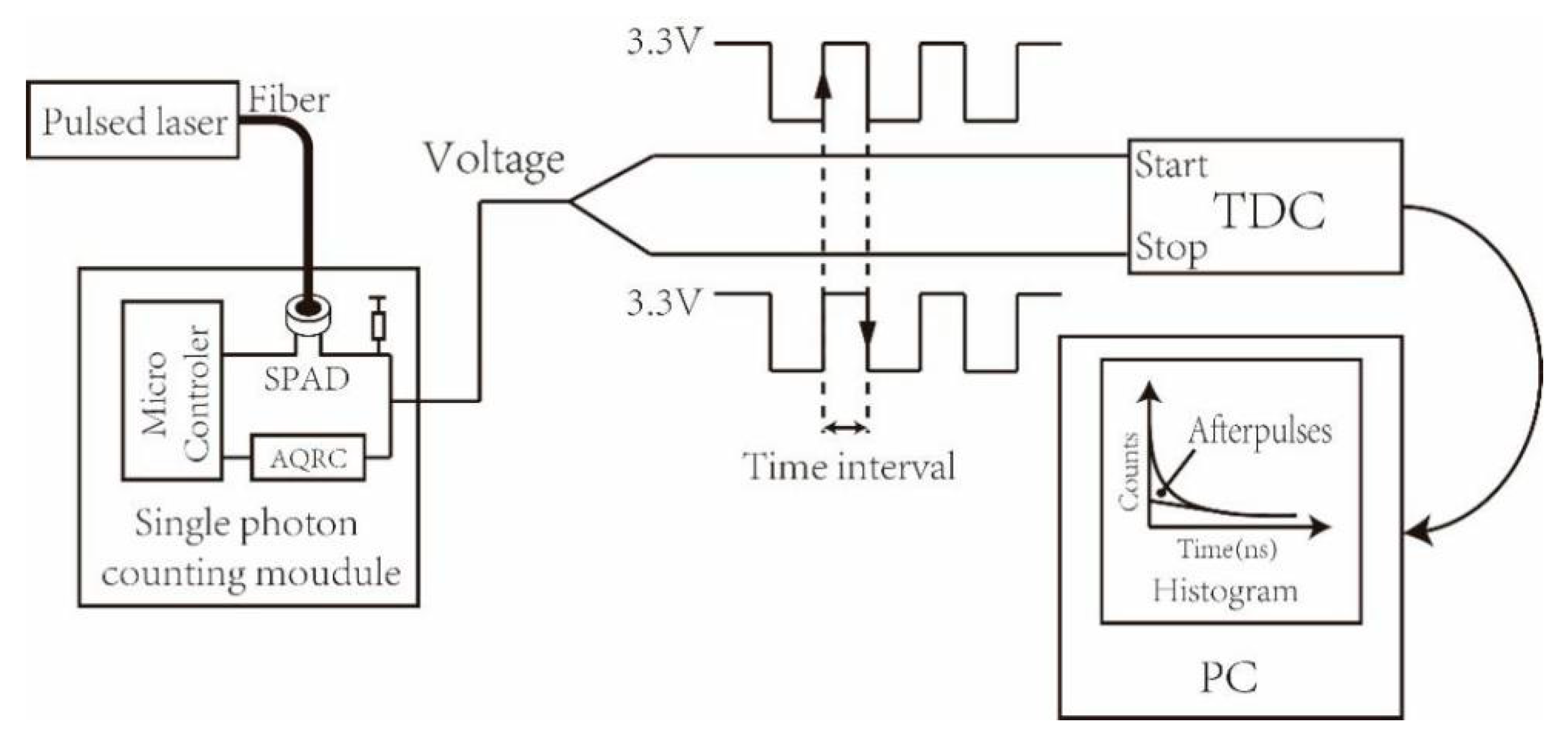
Figure 9 shows the experimental setup for measuring the afterpulsing probability. A pulsed pico-second laser source operating at 10 kHz was used to generate the incident light which was coupled to the SPAD of the module. The laser source used is from ALPHALAS GmbH and the part number of the laser driver and the diode laser are “PLDD-50M” and “PICOPOWER-LD-660-50” respectively. The output of the module is connected to the two ports (start and stop) of a Time-to-digital converter (TDC). The TDC’s “start” channel is triggered by the rising edge of the output pulse of the module and the “stop” channel is triggered by the falling edge of the next neighboring pulse. In this way, the time interval between every two pulses is recorded. After a large amount of data collection (around 10,000 samples), the distribution histogram of the interval times between two adjacent pulses can be built and the afterpulsing probability can be concluded [23,24,25,26].
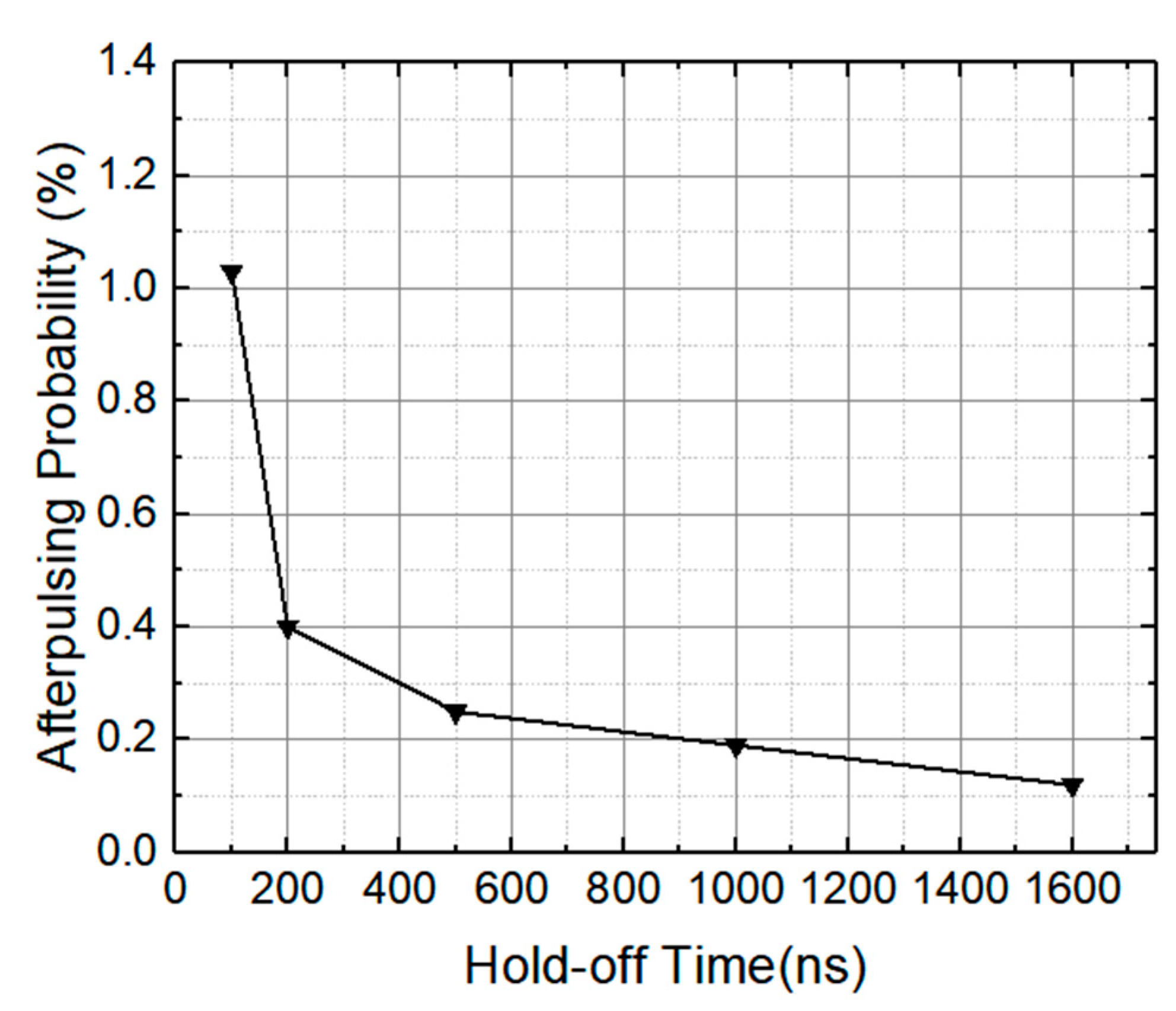
Figure 10 shows the measured afterpulsing probability in the module for different hold-off times with a bias voltage of 27.6 V. Results show that when the hold-off time of the SPAD is set to more than 500 ns, the afterpulsing probability can be significantly limited to below 0.3%. Results also show that as the bias voltage increases, the afterpulsing probability will also rise.
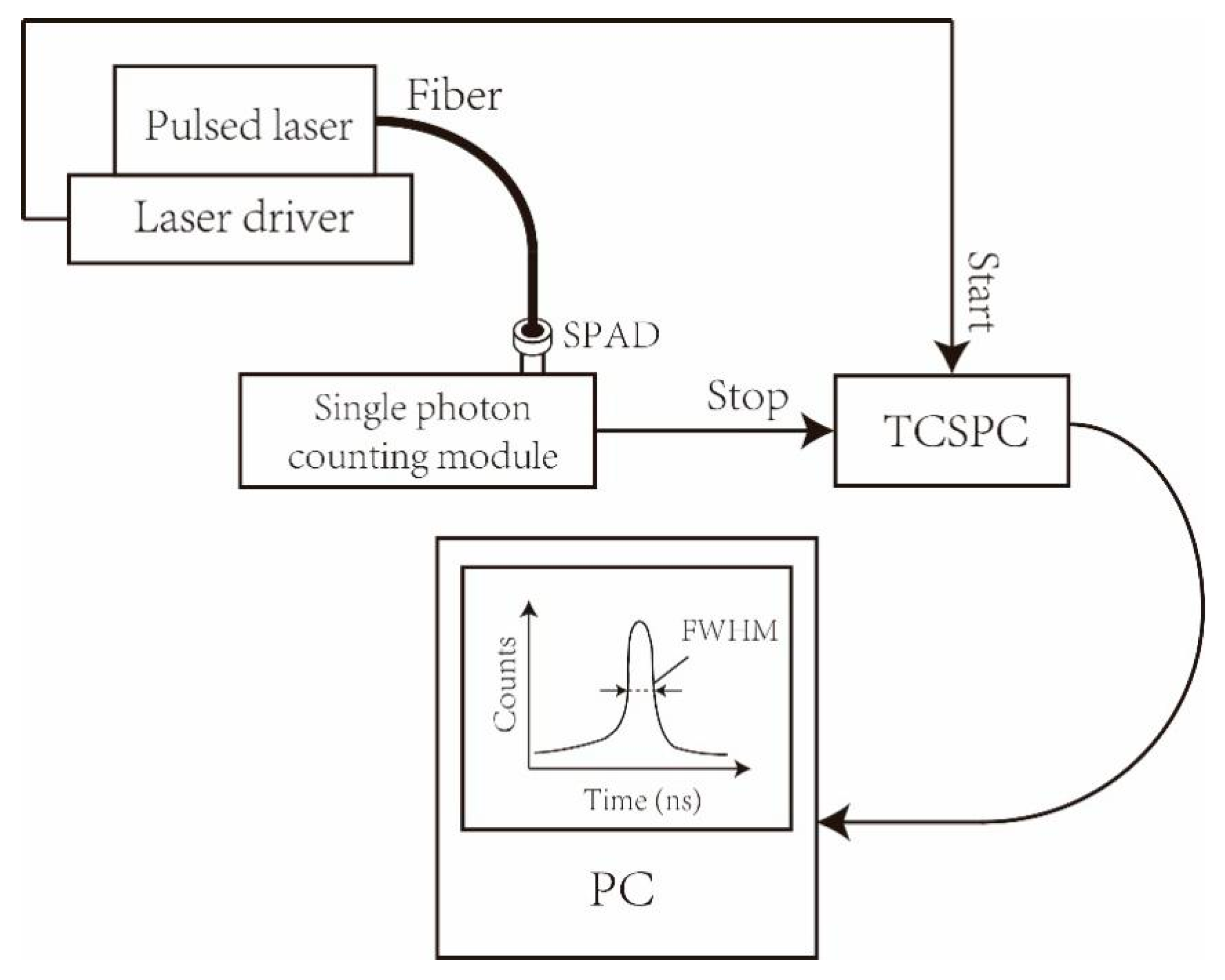
To measure the timing jitter of the module, the experimental setup shown in Figure 11 was built. In the setup, a 660 nm pulsed laser is used to generate a pulsed light signal to the SPAD of the module and the time delay between the laser synchronized pulse signal and the pulses of the module’s output is measured using a TDC. The time delays’ histogram distribution is then built and its full width half maximum (FWHM) is taken as the system’s timing jitter [27].
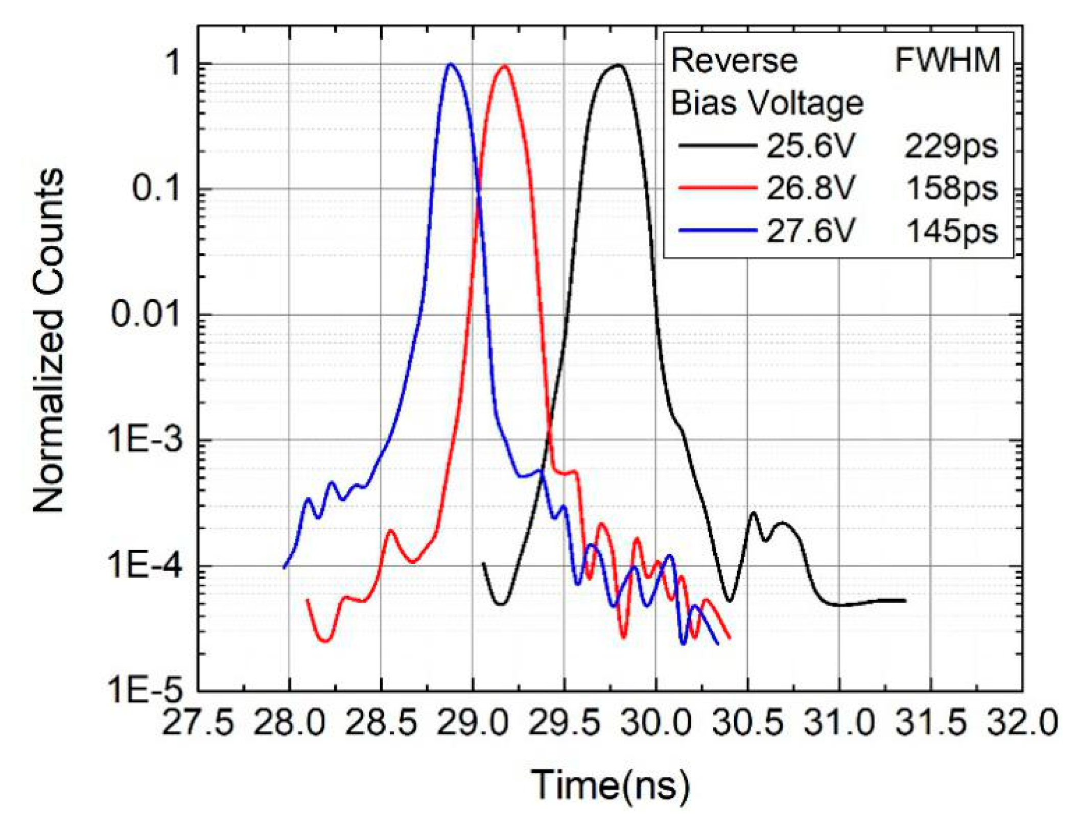
Figure 12 shows the timing responses of the module for different bias voltages. In the measurement, the hold-off time was set to about 200 ns. As can be seen from the figure, increasing the bias voltage results in narrower timing jitter and a timing jitter of 145 ps was measured at the bias voltage of 27.6 V.
To test the heat dissipation of the module, the module was operated continually at room temperature (20 °C) for more than 3 hours and the temperature of the main chips and components on the board (including microcontroller chip, Max749 (boost circuit) chip, USB to TTL chip, DAC chip, 5 V–3 V stabilizer, chip crystal oscillators, SPAD and AQR-IC) was measured. Results show that most the main components are kept cool with the temperature of less than 30 °C.
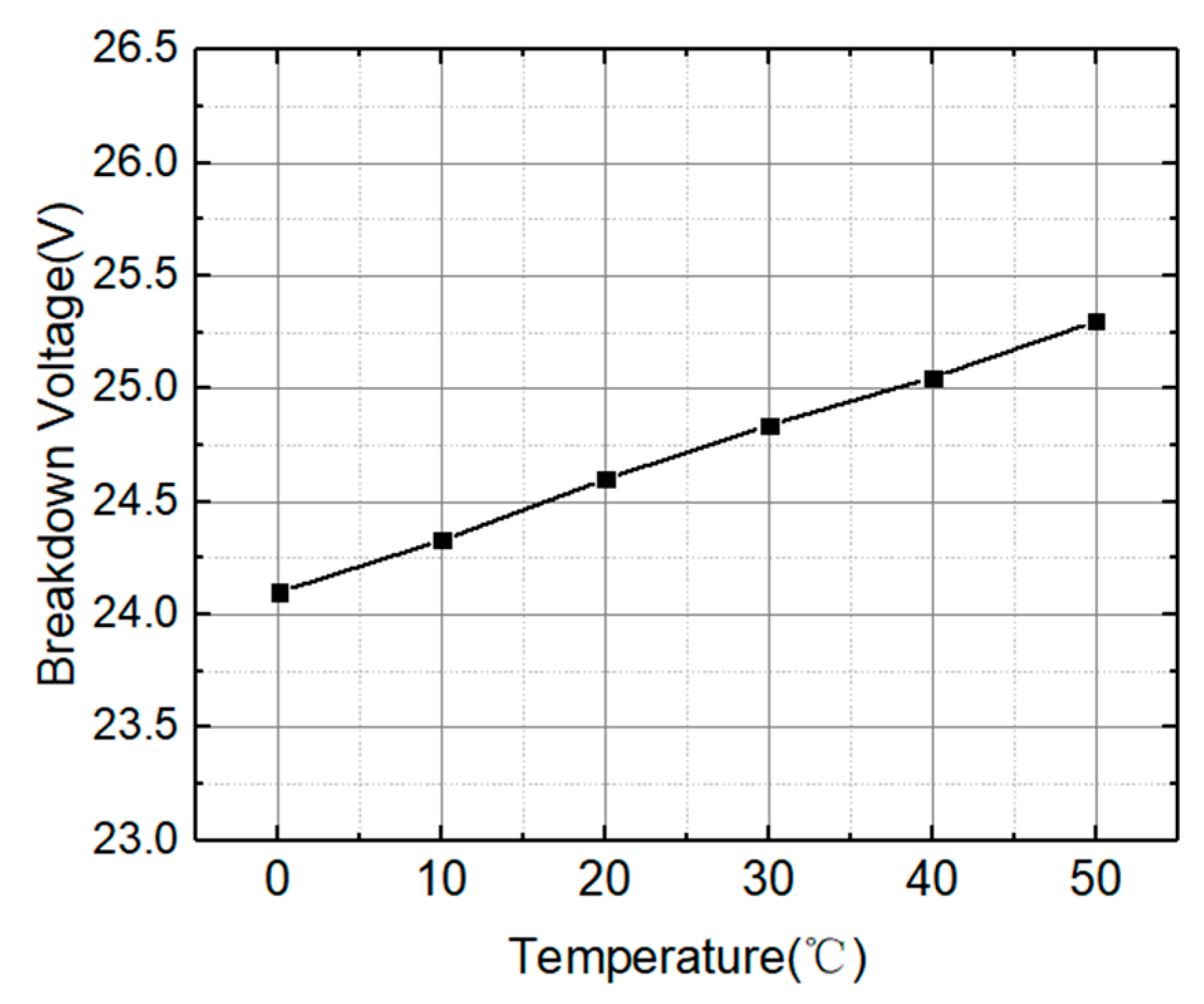
The breakdown voltage and DCR temperature dependency (using a temperature chamber) were also tested. As can be seen from Figure 13, the breakdown voltage of the SPAD rises with increasing temperature at about 0.024 V per °C. Figure 14 shows the plot of the DCR for different temperatures, in this case the excess bias voltage is kept at 1 V. Results show that the DCR increases with increasing temperature by about 23 counts/s per °C.

4. Conclusions

In this paper, the design, the implementation, and the characterization of new compact single-photon counting module is presented. The module enables accurate digital control of the bias voltage and hold-off time of the SPAD. This enables the intelligent optimization of photon detection in varying environments to enhance the module’s robustness. In the system, a programmable negative voltage generator was designed to provide the bias voltage for the SPAD and an active quench and reset chip was developed for the hold-off time control, afterpulsing reduction, and maximum counting rate extension. The new implementation includes a silicon SPAD fabricated in-house is used as the photon detector and a microcontroller system supervises the user interface and the setting of bias voltage and hold-off time. The module is 3.8 cm × 3.6 cm × 2 cm in size and can be powered using a USB connection that allows it to be used in compact single-photon counting applications. Experimental results show that the module can provide a controlled bias voltage for the SPAD from −14 V ~ −38 V with a setting resolution of 0.4 V and the hold-off time (consequently the dead time) in the SPAD from a few nanoseconds to around 1.6 µs with a setting resolution of ∼6.5 ns. Results showed the module can achieve a minimum dead time of 28.5 ns that leads to a maximum counting rate of around 35 Mcounts/s. At a controlled bias voltage of 26.8 V, a low DCR of 300 counts/s and a low timing jitter of 158 ps can be achieved. Results also show that when the hold-off time was set to more than 500 ns, the afterpulsing can be effectively reduced to below 0.3%. In addition, the photodetection probability measurements show that the module is suited for detection of short wavelengths of the light from 450 nm to 800 nm with a 40% peak PDE achieved at 600 nm.

Author Contributions

Conceptualization and methodology, M.C., A.P.M., S.D. and X.X.; SPAD fabrication, A.P.M.; validation, C.L. and C.T.; investigation, C.L., H.L. and H.D.; writing—original draft preparation, S.D. and C.L.; writing—review and editing, A.P.M. and X.X.; supervision, L.Y. and X.X.; funding acquisition, M.C. and X.X. All authors have read and agreed to the published version of the manuscript.

Funding

This research was funded by This work was supported in part by the National Key Research and Development Program of China under Grant 2019YFB2203903, in part by the National Natural Science Foundations of China under Grants, 61827819, 61964005, 61965006, and 61965009, in part by Guangxi Project under Grant AD18281092, AD18281062, AD19245064, 2018GXNSFBA281148, 2019GXNSFBA245057 and 2019GXNSFAA245024, in part by the foundation from Guangxi Key Laboratory of Optoelectronic Information Processing under Grant GD18102, in part by Guangxi Project for ability enhancement of young and middle-aged university teacher under grant 2019KY0211, in part by the foundation from Guangxi Key Laboratory of Automatic Detecting Technology and Instruments under Grant YQ20102, YQ19106 and YQ20107,and in part by Innovation Project of GUET Graduate Education under grant 2020YCXS032.

Conflicts of Interest

The authors declare no conflict of interest. The funders had no role in the design of the study; in the collection, analyses, or interpretation of data; in the writing of the manuscript, or in the decision to publish the results.

References

  1. Tsai, S.-Y.; Chang, Y.-C.; Sang, T.-H. SPAD LiDARs: Modeling and Algorithms. In Proceedings of the 2018 14th IEEE International Conference on Solid-State and Integrated Circuit Technology (ICSICT), Institute of Electrical and Electronics Engineers (IEEE), Qingdao, China, 31 October–3 November 2018; pp. 1–4. [Google Scholar]
  2. Zhang, C.; Lindner, S.; Antolović, I.M.; Pavia, J.M.; Wolf, M.; Charbon, E. A 30-frames/s, 252×144 SPAD Flash LiDAR With 1728 Dual-Clock 48.8-ps TDCs, and Pixel-Wise Integrated Histogramming. IEEE J. Solid-State Circuits 2019, 54, 1137–1151. [Google Scholar] [CrossRef]
  3. Martelli, P.; Brunero, M.; Fasiello, A.; Rossi, F.; Tosi, A.; Martinelli, M. Quantum Key Distribution Exploiting a Faraday Rotator and a Single SPAD. In Proceedings of the 2019 Conference on Lasers and Electro-Optics Europe & European Quantum Electronics Conference (CLEO/Europe-EQEC), Institute of Electrical and Electronics Engineers (IEEE), Munich, Germany, 23–27 June 2019. [Google Scholar]
  4. Gaudin, E.; Arpin, L.; Bouchard, J.; Paille, M.; Bouziri, H.; Bergeron, M.; Pepin, C.M.; Cadorette, J.; Fontaine, R.; LeComte, R. Performance characterization of a dual-threshold time-over-threshold APD-based detector front-end module for PET imaging. In Proceedings of the 2015 IEEE Nuclear Science Symposium and Medical Imaging Conference (NSS/MIC), San Diego, CA, USA, 31 October–7 November 2015; pp. 1–3. [Google Scholar]
  5. Arvani, F.; Carusone, T.C.; Rogers, E.S. TDC Sharing in SPAD-Based Direct Time-of-Flight 3D Imaging Applications. In Proceedings of the 2019 IEEE International Symposium on Circuits and Systems (ISCAS), Sapporo, Japan, 26–29 May 2019; pp. 1–5. [Google Scholar] [CrossRef]
  6. Villa, F.; Lussana, R.; Bronzi, D.; Zappa, F.; Giudice, A. 3D SPAD camera for Advanced Driver Assistance. In Proceedings of the 2017 International Conference of Electrical and Electronic Technologies for Automotive, Torino, Italy, 15–16 June 2017; pp. 1–5. [Google Scholar]
  7. COUNT®. Available online: https://www.lasercomponents.com/us/product/single-photon-counting-modules/ (accessed on 20 May 2020).
  8. PDM Series | PicoQuant. Available online: http://www.picoquant.com/products/category/photon-counting-detectors/pdm-series-single-photon-avalanche-diodes (accessed on 20 May 2020).
  9. Thorlabs. Available online: http://www.thorlabs.de/thorproduct.cfm?partnumber=SPCM50A (accessed on 20 May 2020).
  10. ID100 Visible Single-Photon Detector. Available online: http://www.idquantique.com/photon-counting/photon-counting-modules/id100/ (accessed on 20 May 2020).
  11. Single Photon Counting Modules Excelitas. Available online: http://www.excelitas.com/Pages/Product/Single-Photon-Counting-Modules-SPCM.aspx (accessed on 20 May 2020).
  12. Acconcia, G.; Rech, I.; Labanca, I.; Ghioni, M. 32ps timing jitter with a fully integrated front end circuit and single photon avalanche diodes. Electron. Lett. 2017, 53, 328–329. [Google Scholar] [CrossRef]
  13. Webster, E.A.G.; Grant, L.A.; Henderson, R.K. A High-Performance Single-Photon Avalanche Diode in 130-nm CMOS Imaging Technology. IEEE Electron Device Lett. 2012, 33, 1589–1591. [Google Scholar] [CrossRef]
  14. Berdalović, I.; Osrečki, Ž.; Šegmanović, F.; Grubišić, D.; Knežević, T.; Suligoj, T. Design of passive-quenching active-reset circuit with adjustable hold-off time for single-photon avalanche diodes. In Proceedings of the 2016 39th International Convention on Information and Communication Technology, Electronics and Microelectronics (MIPRO), Opatija, Croatia, 30 May–3 June 2016; pp. 34–39. [Google Scholar]
  15. Ruggeri, A.; Ciccarella, P.; Villa, F.; Zappa, F.; Tosi, A. Integrated Circuit for Subnanosecond Gating of InGaAs/InP SPAD. IEEE J. Quantum Electron. 2015, 51, 1–7. [Google Scholar] [CrossRef] [Green Version]
  16. Giustolisi, G.; Grasso, A.D.; Palumbo, G. Integrated Quenching-and-Reset Circuit for Single-Photon Avalanche Diodes. IEEE Trans. Instrum. Meas. 2014, 64, 271–277. [Google Scholar] [CrossRef]
  17. Liu, J.; Li, Y.; Ding, L.; Wang, Y.; Zhang, T.; Wang, Q.; Fang, J. Fast Active-Quenching Circuit for Free-Running InGaAs(P)/InP Single-Photon Avalanche Diodes. IEEE J. Quantum Electron. 2016, 52, 1–6. [Google Scholar] [CrossRef]
  18. MAX749 Digitally Adjustable LCD Bias Supply. Available online: https://datasheets.maximintegrated.com/en/ds/MAX749.pdf (accessed on 20 May 2020).
  19. Jackson, J.C.; Phelan, D.; Morrison, A.P.; Redfern, R.M.; Mathewson, A. Toward integrated single-photon-counting microarrays. Opt. Eng. 2003, 42, 112–118. [Google Scholar]
  20. Jackson, J.C.; Donnelly, J.; O’neill, B.; Kelleher, A.M.; Healy, G.; Morrison, A.P.; Mathewson, A. Integrated bulk/SOI APD sensor: Bulk substrate inspection with Geiger-mode avalanche photodiodes. Electron. Lett. 2003, 39, 735–736. [Google Scholar] [CrossRef]
  21. Deng, S.; Morrison, A.P. Active quench and reset integrated circuit with novel hold-off time control logic for Geiger-mode avalanche photodiodes. Opt. Lett. 2012, 37, 3876–3878. [Google Scholar] [CrossRef] [PubMed]
  22. Deng, S.; Gordon, D.; Morrison, A.P. A Geiger-Mode APD Photon Counting System With Adjustable Dead-Time and Interchangeable Detector. IEEE Photon-Technol. Lett. 2015, 28, 99–102. [Google Scholar] [CrossRef]
  23. Giudice, A.; Ghioni, M.; Cova, S.; Zappa, F. A process and deep level evaluation tool: Afterpulsing in avalanche junctions. In Proceedings of the Electrical Performance of Electrical Packaging (IEEE Cat. No. 03TH8710), Estoril, Portugal, 16–18 September 2003; pp. 347–350. [Google Scholar]
  24. Humer, G.; Peev, M.; Schaeff, C.; Ramelow, S.; Stipčević, M.; Ursin, R. A simple and robust method for estimating afterpulsing in single photon detectors. J. Light. Technol. 2015, 33, 1. [Google Scholar] [CrossRef] [Green Version]
  25. Ziarkash, A.W.; Joshi, S.K.; Stipčević, M.; Ursin, R. Comparative study of afterpulsing behavior and models in single photon counting avalanche photo diode detectors. Sci. Rep. 2018, 8, 5076. [Google Scholar] [CrossRef] [PubMed] [Green Version]
  26. Palubiak, D.P.; Li, Z.; Deen, J. Afterpulsing Characteristics of Free-Running and Time-Gated Single-Photon Avalanche Diodes in 130-nm CMOS. IEEE Trans. Electron. Devices 2015, 62, 3727–3733. [Google Scholar] [CrossRef]
  27. Villa, F.; Conca, E.; Sesta, V.; Lusardi, N.; Garzetti, F.; Geraci, A.; Zappa, F. SPADs and TDCs for photon-counting, timing and gated-imaging at 30 ps resolution and 60% efficiency. In Proceedings of the 2018 IEEE Nuclear Science Symposium and Medical Imaging Conference Proceedings (NSS/MIC), Sydney, Australia, 10–17 November 2018; pp. 1–5. [Google Scholar]
Figure 1. Block diagram of the single-photon counting module developed.
Electronics 09 01131 g001
Figure 2. Schematic of programmable negative voltage generator.
Electronics 09 01131 g002
Figure 3. Photos of the custom designed and fabricated (a) SPAD and (b) AQR-IC.
Electronics 09 01131 g003
Figure 4. The assembled single-photon counting module.
Electronics 09 01131 g004
Figure 5. (a) The bias voltage boost circuit’s output voltage with the voltage set on computer; (b) External input codes versus hold-off time.
Electronics 09 01131 g005
Figure 6. Experimental setup for the dark count rate and photon detection efficiency measurement.
Electronics 09 01131 g006
Figure 7. Dark count rate measured for varies bias voltages.
Electronics 09 01131 g007
Figure 8. Dependence of photon detection efficiency on the incident wavelength for different bias voltages.
Electronics 09 01131 g008
Figure 9. Experimental setup for measuring SPAD’s afterpulsing probability.
Electronics 09 01131 g009
Figure 10. Afterpulsing probability versus different hold-off times.
Electronics 09 01131 g010
Figure 11. Experimental setup for measuring timing response of the module.
Electronics 09 01131 g011
Figure 12. Timing responses of the single-photon counting module.
Electronics 09 01131 g012
Figure 13. Breakdown voltage measured for various temperatures.
Electronics 09 01131 g013
Figure 14. Dark count rate measured for various temperatures.
Electronics 09 01131 g014