Article

Design of a Low Power 10-b 8-MS/s Asynchronous SAR ADC with On-Chip Reference Voltage Generator

College of Information and Communication Engineering, Sungkyunkwan University, Suwon 16419, Korea
*
Author to whom correspondence should be addressed.
Electronics 2020, 9(5), 872; https://doi.org/10.3390/electronics9050872
Submission received: 8 May 2020 / Revised: 20 May 2020 / Accepted: 21 May 2020 / Published: 24 May 2020
(This article belongs to the Special Issue Analog/Digital Mixed Circuit and RF Transceiver Design)

Abstract

:
This paper presents an energy-efficient low power 10-b 8-MS/s asynchronous successive approximation register (SAR) analog-to-digital (ADC) converter. An inverted common-mode charge recovery technique is proposed to reduce the switching energy and to improve the linearity of the digital-to-analog converter (DAC). The proposed switching technique consumes only 149 CVREF2 switching energy for the 10-bit case. A rail-to-rail dynamic latch comparator is implemented with adaptive power control for better power efficiency. Additionally, to optimize the power consumption and performance of the logic part, a modified asynchronous type SAR control logic with digitally controllable delay cells is adopted. An on-chip reference voltage generator is also designed with an ADC core for practical use. The structure is realized using 55-nm complementary metal–oxide–semiconductor (CMOS) process technology. The proposed architecture achieves an effective number of bits (ENOB) of 9.56 bits and a signal-to-noise and distortion ratio (SNDR) level of 59.3 dB with a sampling rate of 8 MS/s at measurement level. The whole architecture consumes only 572 µW power when a power supply of 1 V is applied.

1. Introduction

Successive approximation register (SAR) analog-to-digital converters (ADCs) have emerged as the best option for meeting the requirement of low power consumption, high speed, and medium resolution among different ADC architectures. Excellent power efficiency and reduced analog complexity make SAR ADCs the best choice for low power applications [1,2,3,4]. Effective number of bits (ENOB), power consumption, and conversion speed along with other parameters measure the performance of ADCs. With complementary metal–oxide–semiconductor (CMOS) technologies entering the submicron domain, the transistor sizing has been downscaled to a few nanometers [5,6,7,8,9]. For low power and medium conversion speed, the SAR type ADC is among the best available choices as in its operation, full conversion is divided into several comparison phases by using only one comparator [10].
The SAR control logic uses the binary search algorithm, performs the analog-to-digital conversion process over multiple clock cycles by going through all possible bits, and determines the next bit based on the information of the previous bit. In a conventional synchronous SAR ADC, the sampling process and all conversion steps are done according to an external clock. Therefore, it needs at least (N + 1) number of clock cycles to complete its operation and produce the output for an N bit ADC. Hence, it needs (N + 1) times faster clock frequency than its sampling rate, which makes its operation non-viable for higher speed. Back-to-back execution with internally generated control signals makes asynchronous SAR ADC much faster than synchronous SAR ADC [11]. To reduce the switching energy and area of a capacitive digital-to-analog converter (DAC), many capacitor-switching schemes have been presented in the literature [12,13,14,15,16]. Although these switching schemes have achieved good results, there are still improvements to be addressed regarding enhanced linearity and parasitic effects.
This work aims to provide an architecture in which several techniques and strategies are used to optimize the power efficiency, area, and speed. An inverted common-mode charge recovery (ICMCR) switching technique is implemented to decrease the switching energy from the capacitive DAC. The proposed switching technique consumes only 149 CVREF2 switching energy for the 10-bit case. An adaptive power control (APC) circuit is employed with a modified rail-to-rail dynamic latch comparator, which controls the comparator’s operation and reduces its active time and, hence, results in reduction in overall power consumption. An asynchronous SAR logic with controllable delays is introduced for a faster and less power-consuming operation. Additionally, an on-chip reference voltage generator is implemented to avoid off-chip power hungry references complexity. This paper focuses on reduction in power consumption and the optimization of area and speed of SAR ADC.
In Section 2, we discuss the main architecture for asynchronous SAR ADC. Section 3 explains sub-blocks of the ADC including circuit design implementation of the capacitive DAC, rail-to-rail dynamic latch comparator with APC control, and asynchronous dynamic logic with the loop delay technique for the power-efficient implementation of digital logic. The on-chip reference voltage generator is presented in Section 4, and simulation/measurement results are discussed in Section 5. Finally, Section 6 concludes the paper.

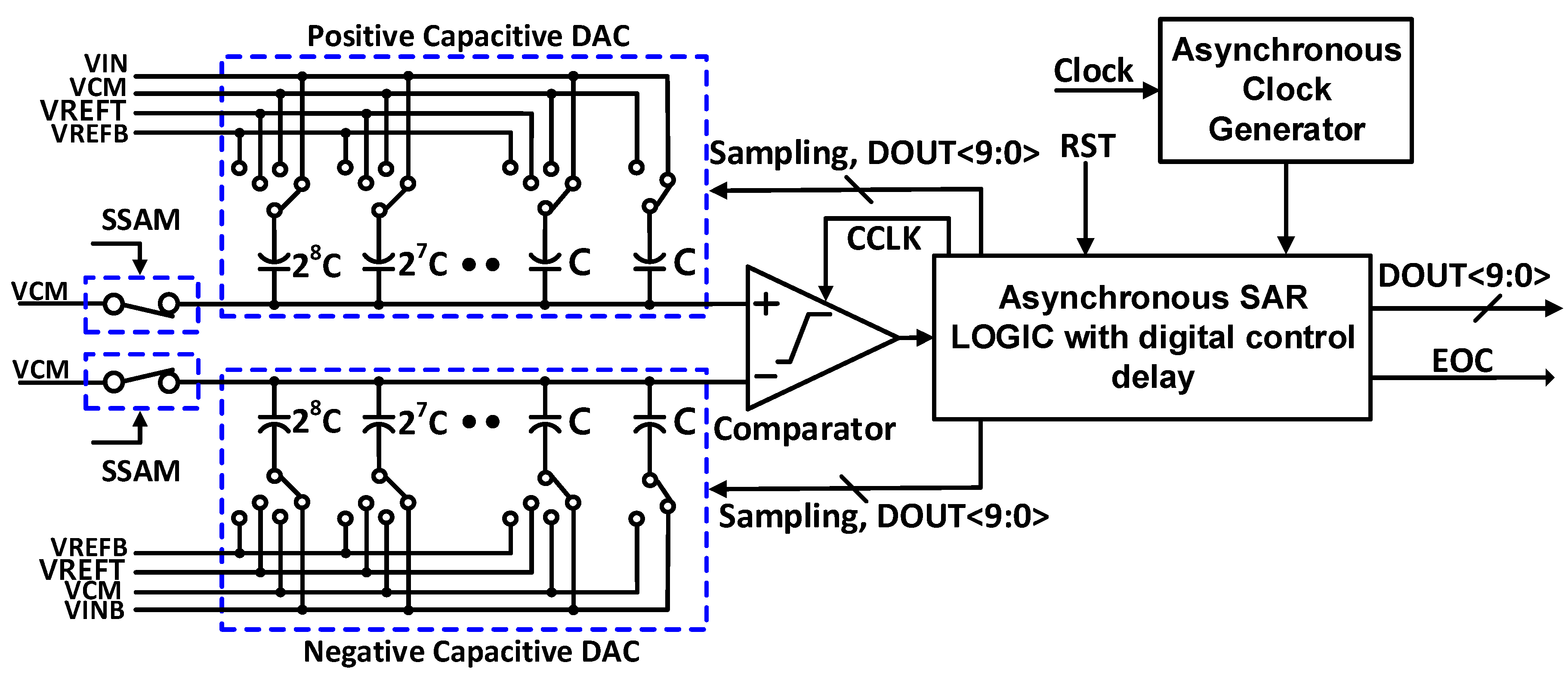
2. The Proposed ADC Architecture

The proposed prototype of 10-bit SAR ADC is composed of a reference voltage generator and ADC core consisting of a capacitive DAC part, a dynamic latch comparator with APC, and asynchronous SAR logic, as shown in Figure 1. Unlike the synchronous SAR ADC, only 8 MHz clock frequency is applied to achieve a sampling rate of 8 MS/s. A typical asynchronous SAR control has a fixed delay for each comparison, which leads to wasted time during the comparison process. This time can be adjusted, as the most significant bit (MSB) capacitor requires longer settling as compared to the least significant bit (LSB) capacitor. For this purpose, digitally controlled delays are introduced to control the conversion time of each bit. An inverted common-mode charge recovery (ICMCR) technique is proposed to reduce the switching energy from the capacitive DAC. This improves the linearity of the capacitive DAC by reducing the effect of parasitic capacitances. The proposed switching technique consumes only 149 CVREF2 switching energy for the 10-bit case. A 0.5 fF custom-designed metal–oxide–metal unit capacitor is designed to be used in the capacitive DAC to optimize the area and current consumption. Moreover, an APC circuit is added to the comparator, which turns off the comparator when the comparison is made.

3. Circuit Implementation

3.1. Capacitive DAC

Among non-calibrated capacitive DAC switching techniques, the common-mode based charge recovery (CMCR) technique has proven to be one the most energy-efficient techniques [12]. The CMCR scheme provides one more bit resolution as compared to the other schemes by requiring half of the total capacitance of the other schemes. In this technique, a fixed common-mode voltage leads to the simplification of the comparator’s design, resulting in improved linearity. An optimized use of common-mode level during the conversion process in presented in [16]. However, CMCR shows sensitivity to the parasitic capacitance because during the conversion process, the voltage on the top plate does not return to the same voltage from which it began. To overcome this issue of sensitivity to parasitic capacitances without any energy trade-off, an inverted common-mode charge recovery (ICMCR) technique is implemented. For the explanation of the proposed algorithm, a 3-bit example is shown in Figure 2. The key idea is to invert the sampling, by sampling VCM on the top plates and the inputs on the bottom plates of the capacitive DAC, then both inputs VIP and VIN are disconnected from the capacitive DAC and for the first comparison, VCM is applied to the bottom plates of the capacitive DAC. Without costing additional energy, the ICMCR technique ensures that the voltages on the top plates of the capacitive DAC begin and end at the same voltage, VCM, thereby eliminating the sensitivity to parasitic capacitances on that node as well as the signal dependence of charge injection. The current code and the previous code together determine the energy required for each conversion. In this case, the energy per code is EVREF = CVREF2 / 2, where C is the unit capacitor used for LSB, and the other capacitors from LSB to MSB are multiples of C. The energy consumption in the proposed ICMCR scheme is proportional to (C × VREF2 / 2), and it consumes only 149 CVREF2 switching energy for the 10-bit case.

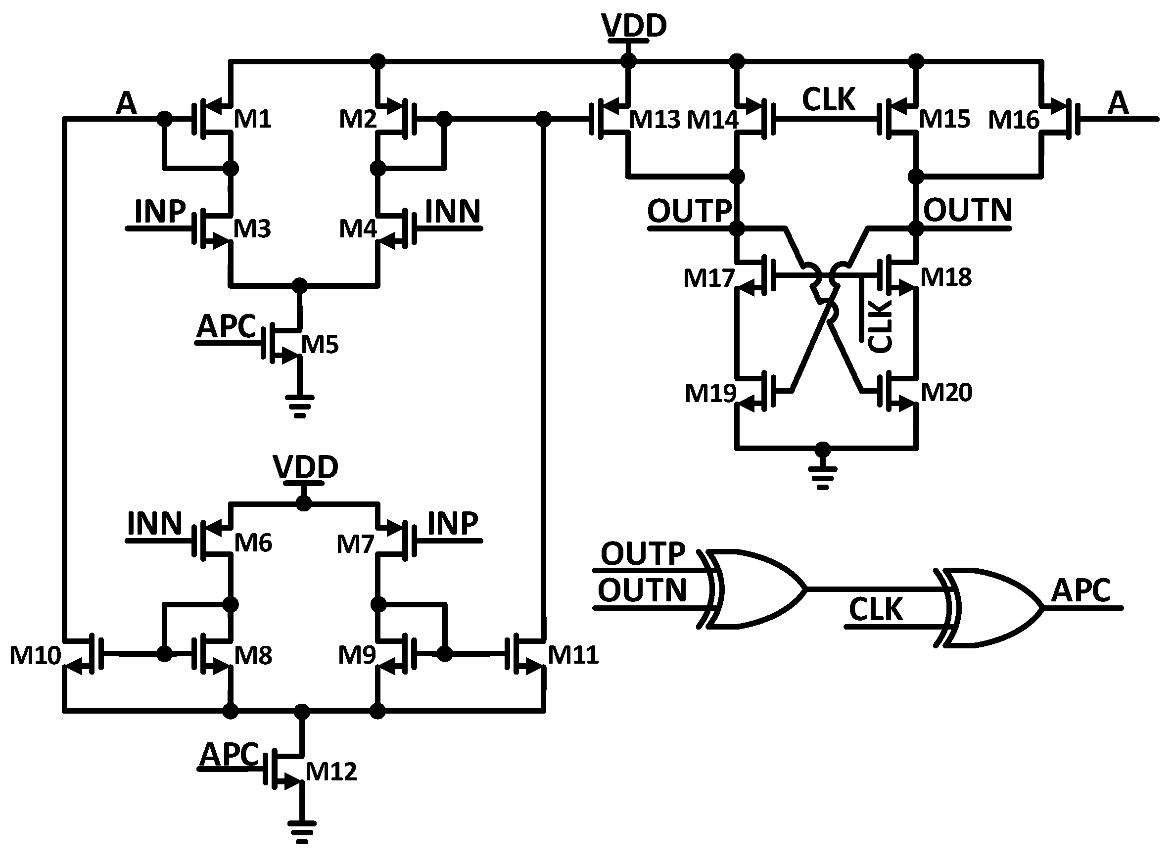
3.2. Rail-to-Rail Dynamic Latch Comparator with APC

The architecture of the proposed rail-to-rail dynamic latch comparator with the APC topology, which uses two exclusive OR (XOR), is depicted in Figure 3. Transistors M1, M2, M3, M4, M6, M7, M8, and M9 make the preamplifier, and the transistors M13, M16, M19, and M20 make the dynamic latch in the second stage. Transistors M3, M4, M6, and M7 make the input differential amplifier architecture for the rail-to-rail input range.
To ensure that there is no static current in the reset phase, the clock (CLK) is zero; the transistors M17, M18, M5, and M12 turn off; and the transistors M14 and M15 turn on. In the evaluation phase, CLK is one; the transistors M14 and M15 turn off; and transistors M17, M18, M5, and M12 turn on. In the beginning of the evaluation phase, the differential input pair and the latch stage are in conduction mode. For the regenerative dynamic latch stage, differential input voltage is transformed into the identical differential current. Strong positive feedback of the latch helps to regenerate the small differential input voltage into a full swing output voltage. When the evaluation phase is completed, the output stimulates the adaptive power control block, and when CLK is 0, output nodes OUTP and OUTN go to the power source voltage (VDD) by reset transistors M14 and M15. As a consequence, the output of the first XOR gate is 0. The output of the second XOR gate comes after the input CLK. APC signal changes to high logic level, when CLK goes from zero to one. When APC signal is high, the preamplifier turns on. After the evaluation is completed, one of the output nodes goes to VDD and the other node goes to ground, and the output of XOR becomes high. After this, the APC signal turns into low logic state because both the input terminals of the second XOR are high. Once the APC signal becomes low, it turns off the DC supply of the preamplifier.

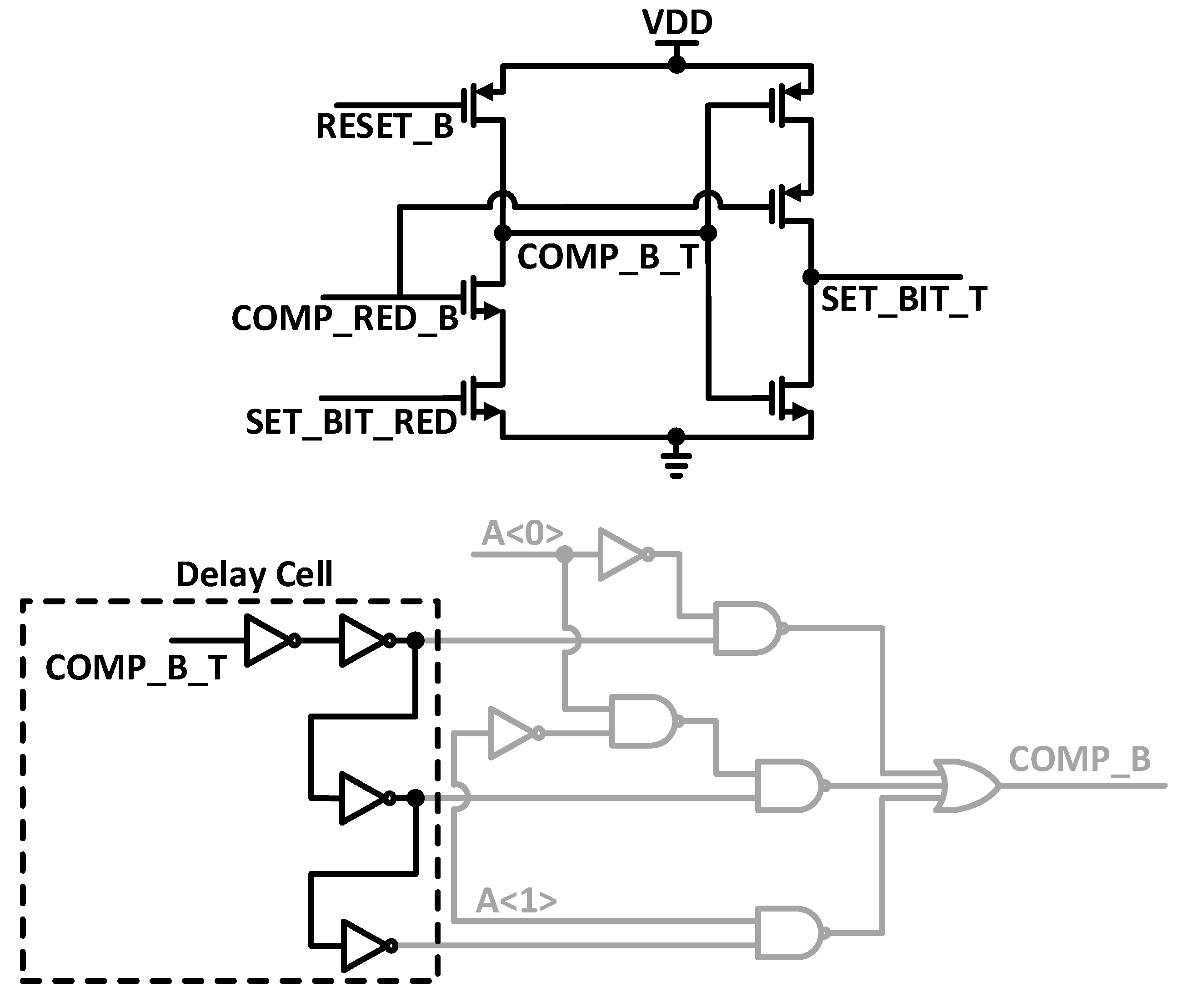
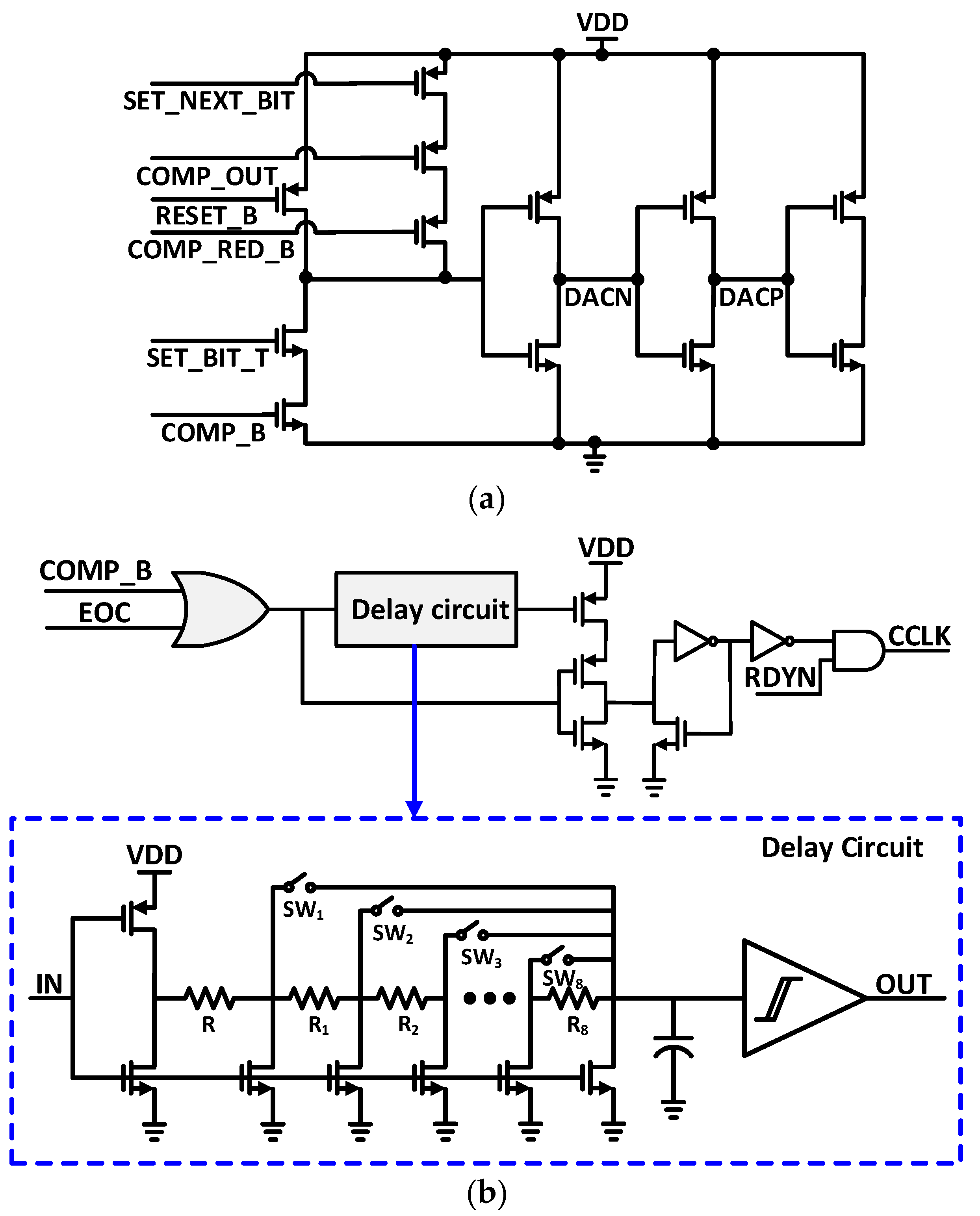
3.3. Asynchronous SAR Logic with Digital Control Delays

In the proposed architecture, an asynchronous controller is used in SAR logic to optimize the power consumed by the logic part. Asynchronous SAR logic minimizes the power consumption by eradicating the necessity of high speed clock generation. Instead, it generates the control signals internally, which do not need global synchronization for every bit cycle. Additionally, a modified asynchronous type control logic is adopted to digitally control the delay between DAC switching and the comparator’s operation. Unlike the synchronous logic, it does not need a fixed delay for each cycle but a different controllable delay for each bit cycle from LSB to MSB.
In current dynamic logic, the combinational logics used in the digital control part are implemented by using the transistors to reduce the complexity. Asynchronous control is composed of a main control block and a DAC control with an asynchronous clock generator. The timing diagram of logic is shown in Figure 4. Once the clock (CLK) goes high, the comparator starts the comparison process based on the comparator clock (CCLK) generated by the DAC control with the asynchronous clock generator block. When the comparison for LSB is made, the loop resets the comparator and an end of conversion (EOC) signal is generated. Main control with the DAC delay circuit is shown in Figure 5, which can be externally controlled by digital signal A<1:0>. Dynamic logic implementation is carried out to minimize the complexity of the circuit and power consumption of the logic block, as the same functionality can be achieved with fewer transistors than the complementary logic [17]. DAC control of SAR logic is shown in Figure 6a.
The loop delay circuit has a property that is divided into the comparator reset path and DAC settling path based upon the COMP_B. These two operations can use both slow and fast signal flow. Nevertheless, the delay cell’s internal node can be in an undesired state when the delay cell input has a low state, because the input of the delay cell may change before the internal logical states have been entirely propagated by earlier high state inputs. Reset switches added to avert these unsettled states in the presented delay cell are shown in Figure 6b. When the reset path of the comparator is activated, reset switches swiftly reset the internal nodes of the delay cell. A 3-bit digital input controls the delay cell, and eight switches and resistors are used in the presented delay cell. A larger resistance, to increase the minimum delay, replaces R, representing the first passive resistance. To prevent the glitch caused by the supply oscillation, a Schmitt trigger is used at the output stage [18].

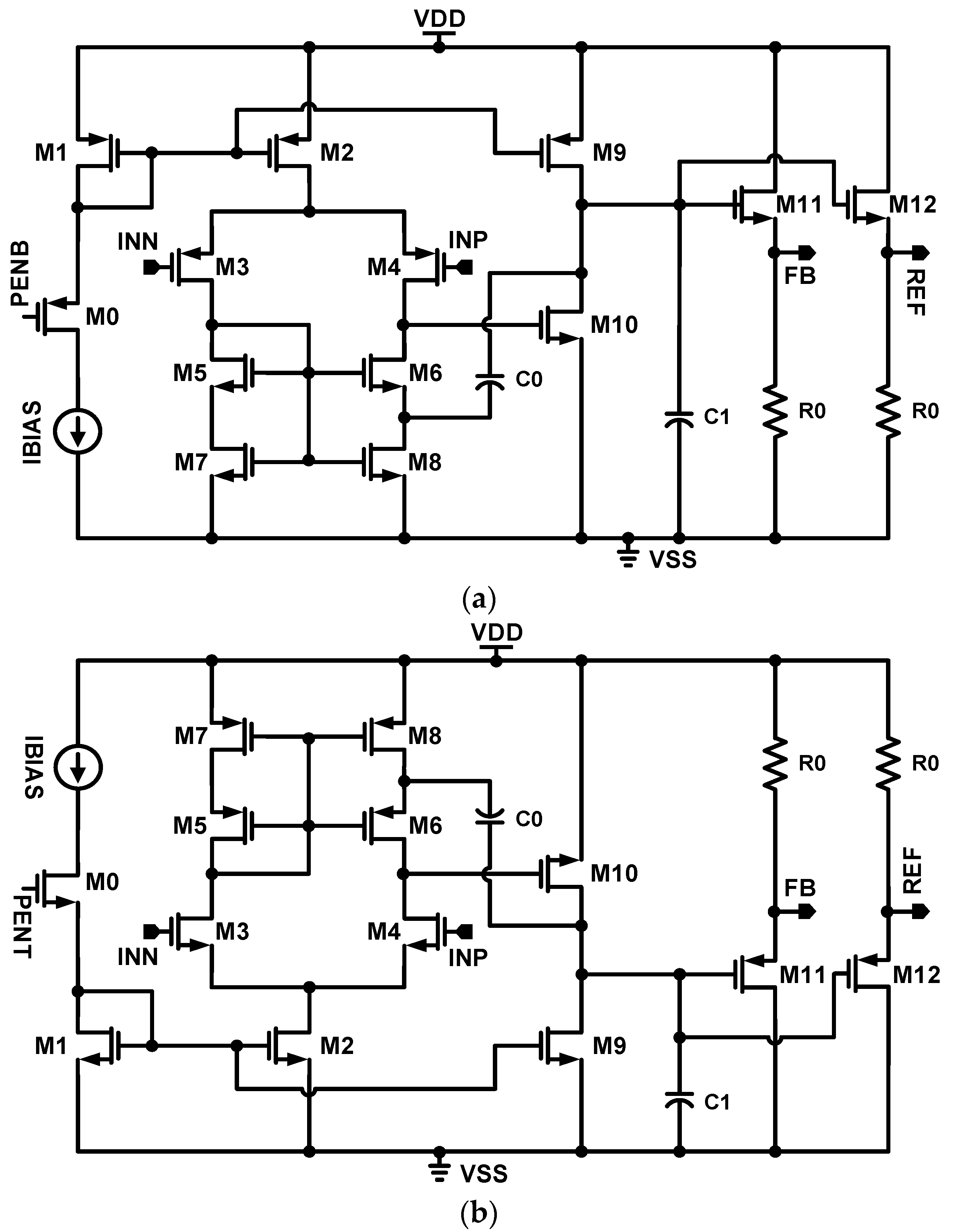
4. Reference Voltage Generator

In most ADCs, the stability of the reference voltages plays a major role in the resolution. In this regard, reference voltages should be a fixed value regardless of the process, voltage, and temperature (PVT) variation. The reference generator provides the following voltages: VREFB of 0.2 V, VCM of 0.5 V, and VREFT of 0.8 V. Moreover, trimming is added in the reference voltage generator to compensate for the difference in the results and voltage mismatch. VREFT can be trimmed to between 0.65 V and 0.8 V, VREFB can be trimmed to between 0.2 V and 0.35 V, and VCM can be varied from 0.425 V to 0.575 V. The architecture of reference voltage generator is shown in Figure 7. Band-gap reference voltage (VBGR) has been used as the input of the reference voltage generator, and to compensate for the variations and mismatch, trimming controls have been added for each reference voltage.
To reduce the overall cost, size, and power consumption, on-chip reference voltage buffers are preferred in system–on–chip (SoC) design. To achieve fast settling, a buffer with very low output resistance is required. The schematic of the reference voltage buffers used in the current design is shown in Figure 8. There is a two-stage structure followed by two source-follower (SF) stages with nodes FB and REF. One replica SF stage separates the FB node from the capacitive load as well as provides a feedback loop, ensuring stability. On the other hand, the open loop settling from the other replica SF stage ensures faster operation. In the conventional two-stage structure, Miller compensation with a larger trans-conductance is required in the second stage, which increases the power consumption. Additionally, a resistor is used to avoid the degradation in the phase margin. To overcome these issues, an indirect method of compensation has been adopted using split-length devices [19].

5. Simulation and Measurement Results

5.1. Simulation Results

Figure 9 depicts the capacitive DAC outputs (OUTP and OUTN) settling for maximum and minimum values of input signals according to the clock signal. Based on the asynchronous SAR logic, when the conversion cycle is completed it generates an end of conversion (EOC) signal.
Figure 10 shows the simulation results of the reference voltage generator. The required reference voltages VREFT, VCM, and VREFB for ADC core operation are 0.8 V, 0.5 V, and 0.2 V, respectively. For each voltage level, trimming is added to achieve an optimum performance level. VREFT trimming provides 0.65–0.8 V, VCM can be controlled between 0.425 V and 0.575 V, and VREFB from 0.2 V to 0.35 V can be achieved through control trim bits.
Figure 11 shows the Monte Carlo simulation of the reference voltage generator. In the proposed architecture, an on-chip reference voltage generator is used with a standard deviation of reference voltage that is less than 1 LSB. The ADC core is designed to receive a reference voltage of 0.8 V, 0.5 V, and 0.2 V, respectively. When switching from initial input sampling interval to redistribution mode, the DAC voltage will vary up to 0.3 V, then the ADC core MSB decision time is divided so that settling time can be sufficient for switching.

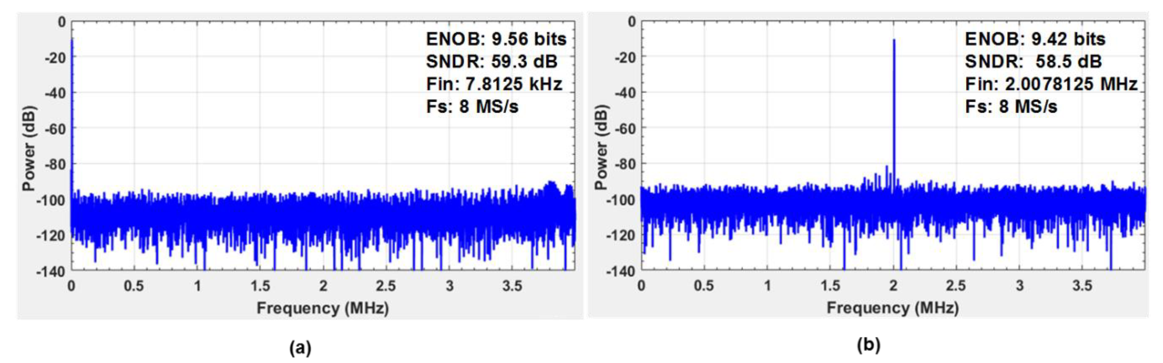
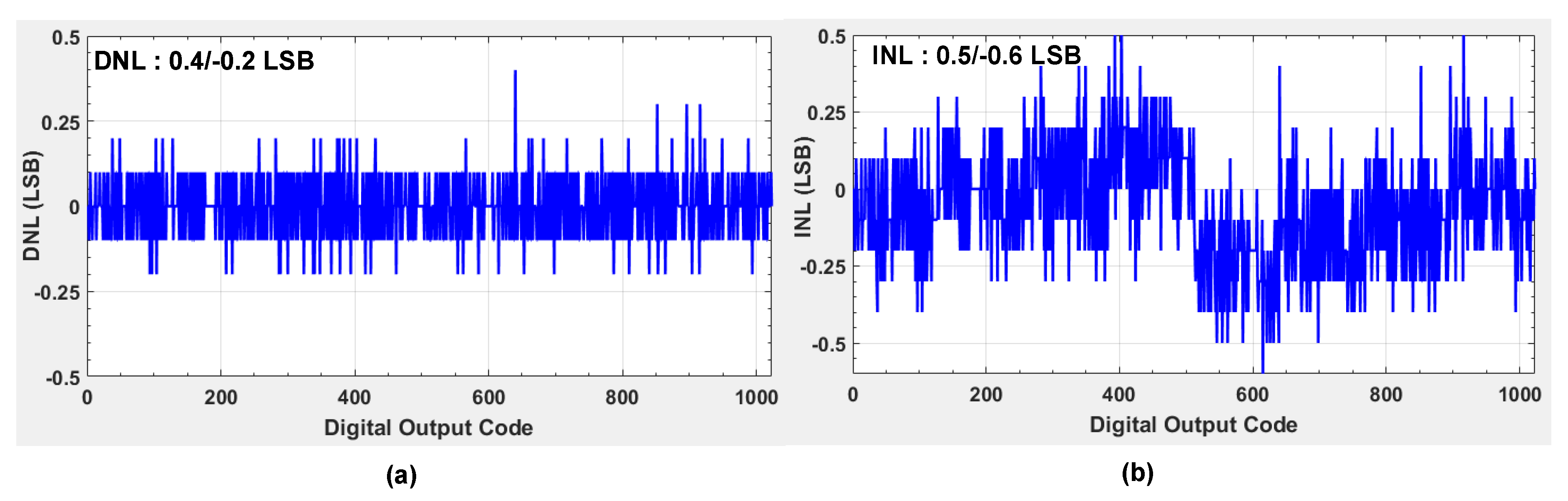
5.2. Measurement Results

The presented structure is fabricated and tested with 55-nm CMOS technology. Figure 12 shows the measured dynamic performance of ADC at different frequencies. It achieves an ENOB of 9.56 bits at the sampling frequency of 8 MS/s and an input range with a peak-to-peak value of 600 mV. Figure 13 shows the differential non-linearity (DNL) and integral non-linearity (INL) results to represent the static performance of ADC, which are 0.4 to −0.2 and 0.5 to −0.6, respectively.
The measured performance of the presented structure and comparison with other SAR ADC architectures, [17] and [20,21,22,23], are summarized in Table 1. To evaluate the power efficiency, the typical parameter, Figure of Merit (FOM), is used as:
FOM = Power 2 ENOB × FS
where FS represents the sampling frequency and Power denotes the power consumption. The proposed ADC shows a FOM of 94.72 fJ/step. The proposed design shows very good power efficiency as compared to other 10-bit SAR ADCs.

6. Conclusions

This paper presents a low power 10-bit asynchronous SAR ADC with an on-chip reference voltage generator operating at a sampling rate of 8 MS/s. A custom-designed metal–oxide–metal capacitor with a smaller size has been used as a unit capacitor in the capacitive DAC to minimize the area and power of the analog part. An inverted common-mode charge recovery technique is proposed to reduce the switching energy from the capacitive DAC. It consumes only 149 CVREF2 switching energy. The proposed switching technique improves the linearity by reducing the effect of parasitic capacitances. It has an unchanged common-mode voltage level regarding the comparator, which eases the design of the comparator. Moreover, a modified rail-to-rail dynamic latch comparator with adaptive power control has been implemented to enable fast operation and good resolution. The comparator’s operation is controlled by the APC circuit, which results in an improved power efficiency. A modified asynchronous control logic with scalable delays for each comparison is adopted in the presented ADC. For practical use support, the top block is designed with a low power reference voltage generator to drive the ADC core. The ADC is fabricated in a 55-nm CMOS process, and it achieves an FoM of 94.7 fJ/conv-step. The measurement results show that the proposed circuit achieves an ENOB of 9.56 bits and SNDR of 59.3 dB when operated at 8 MS/s with 1 V supply.

Author Contributions

Conceptualization, K.S. and D.V.; methodology, K.S.; software, K.S, D.V., and Q.U.A.; validation, K.S., D.V., and S.J.K.; formal analysis, K.S., D.V., and S.J.K.; investigation, K.S., D.V., and M.B.; resources, K.S.; data curation, K.S. and D.V.; writing—original draft preparation, K.S. and K.-Y.L.; writing—review and editing, K.S., D.K., Y.P. and K.-Y.L.; visualization, K.S., D.V., D.K., and K.-Y.L.; supervision, K.C.H., Y.Y., and K.-Y.L.; project administration, K.-Y.L. All authors have read and agreed to the published version of the manuscript.

Funding

This research received no external funding.

Acknowledgments

This research was supported by the MOTIE (Ministry of Trade, Industry & Energy) (10080622) and KSRC (Korea Semiconductor Research Consortium) support program for the development of the future semiconductor device.

Conflicts of Interest

The authors declare no conflict of interest.

References

  1. Kim, S.J.; Kim, D.G.; Oh, S.J.; Lee, D.S.; Pu, Y.; Hwang, K.C.; Yang, Y.; Lee, K.-Y. A Fully Integrated Bluetooth Low-Energy Transceiver with Integrated Single Pole Double Throw and Power Management Unit for IoT Sensors. Sensors 2019, 19, 2420. [Google Scholar] [CrossRef] [PubMed] [Green Version]
  2. Shim, J.; Kim, M.-K.; Hong, S.-K.; Kwon, O.-K. A low-power single-ended 11-bit SA-ADC with 1 V supply voltage and 2 V input voltage range for CMOS image sensors. In Proceedings of the 2016 IEEE Asia Pacific Conference on Circuits and Systems (APCCAS), Jeju, Korea, 25–28 October 2016; pp. 410–413. [Google Scholar]
  3. Chen, S.-L.; Villaverde, J.F.; Lee, H.-Y.; Chung, D.W.-Y.; Lin, T.-L.; Tseng, C.-H.; Lo, K.-A. A Power-Efficient Mixed-Signal Smart ADC Design With Adaptive Resolution and Variable Sampling Rate for Low-Power Applications. IEEE Sens. J. 2017, 17, 3461–3469. [Google Scholar] [CrossRef]
  4. Shehzad, K.; Kang, H.-Y.; Verma, D.; Park, Y.J.; Lee, K.-Y. Low-power 10-bit SAR ADC using class-AB type amplifier for IoT applications. In Proceedings of the 2017 International SoC Design Conference (ISOCC), Seoul, Korea, 5–8 November 2017; pp. 224–225. [Google Scholar]
  5. Giannini, V.; Nuzzo, P.; Chironi, V.; Baschirotto, A.; van der Plas, G.; Craninckx, J. An 820µW 9b 40MS/s Noise-Tolerant Dynamic-SAR ADC in 90nm Digital CMOS. In Proceedings of the 2008 IEEE International Solid-State Circuits Conference—Digest of Technical Papers, San Francisco, CA, USA, 3–7 February 2008; pp. 238–239. [Google Scholar]
  6. Rikan, B.S.; Kim, S.; Abbasizadeh, H.; Hejazi, A.; Rad, R.E.; Shehzad, K.; Hwang, K.C.; Yang, Y.; Lee, M.; Lee, K.-Y. A 10- and 12-Bit Multi-Channel Hybrid Type Successive Approximation Register Analog-to-Digital Converter for Wireless Power Transfer System. Energies 2018, 11, 2673. [Google Scholar] [CrossRef] [Green Version]
  7. Scholtens, P.; Vertregt, M. A 6b 1.6 Gsample/s flash ADC in 0.18 /spl mu/m CMOS using averaging termination. In Proceedings of the 2002 IEEE International Solid-State Circuits Conference. Digest of Technical Papers, San Francisco, CA, USA, 7 February 2002; Volume 1, pp. 168–457. [Google Scholar]
  8. Wang, D.; Zhu, X.; Guo, X.; Luan, J.; Zhou, L.; Wu, D.; Liu, H.; Wu, J.; Liu, X. A 2.6 GS/s 8-Bit Time-Interleaved SAR ADC in 55 nm CMOS Technology. Electronics 2019, 8, 305. [Google Scholar] [CrossRef] [Green Version]
  9. Verma, D.; Kang, H.Y.; Shehzad, K.; Rehman, M.R.U.; Lee, K.-Y. Design of asynchronous SAR ADC for low power mixed signal applications. In Proceedings of the 2017 International SoC Design Conference (ISOCC), Seoul, Korea, 5–8 November 2017; pp. 222–223. [Google Scholar]
  10. Xin, X.; Cai, J.; Xie, R.; Wang, P. Ultra-low power comparator with dynamic offset cancellation for SAR ADC. Electron. Lett. 2017, 53, 1572–1574. [Google Scholar] [CrossRef]
  11. Huang, C.P.; Lin, J.M.; Shyu, Y.T.; Chang, S.J. A Systematic design methodology of asynchronous SAR ADCs. IEEE Trans. Very Large Scale Integr. VLSI Syst. 2016, 24, 1835–8148. [Google Scholar] [CrossRef]
  12. Liu, C.-C.; Chang, S.-J.; Huang, G.-Y.; Lin, Y.-Z. A 10-bit 50-MS/s SAR ADC with a Monotonic Capacitor Switching Procedure. IEEE J. Solid State Circuits 2010, 45, 731–740. [Google Scholar] [CrossRef]
  13. Zhu, Y.; Chan, C.-H.; Chio, U.-F.; Sin, S.-W.; Seng-Pan, U.; Martins, R.P.; Maloberti, F. A 10-bit 100-MS/s Reference-Free SAR ADC in 90 nm CMOS. IEEE J. Solid State Circuits 2010, 45, 1111–1121. [Google Scholar] [CrossRef]
  14. Lu, C.-C.; Huang, D.-K. A 10-Bits 50-MS/s SAR ADC Based on Area-Efficient and Low-Energy Switching Scheme. IEEE Access 2020, 8, 28257–28266. [Google Scholar] [CrossRef]
  15. Verma, D.; Shehzad, K.; Khan, D.; Ain, Q.U.; Kim, S.J.; Lee, D.; Pu, Y.G.; Lee, M.; Hwang, K.C.; Yang, Y.; et al. A Design of 8 fJ/Conversion-Step 10-bit 8MS/s Low Power Asynchronous SAR ADC for IEEE 802.15.1 IoT Sensor Based Applications. IEEE Access 2020, 8, 85869–85879. [Google Scholar] [CrossRef]
  16. Guerber, J.; Venkatram, H.; Oh, T.; Moon, U.-K. Enhanced SAR ADC energy efficiency from the early reset merged capacitor switching algorithm. In Proceedings of the 2012 IEEE International Symposium on Circuits and Systems (ISCAS), Seoul, Korea, 20–23 May 2012; pp. 2361–2364. [Google Scholar] [CrossRef]
  17. Verma, D.; Shehzad, K.; Kim, S.J.; Lee, K.-Y. Low Power 10-BIT 8MS/s Asynchronous SAR ADC with Wake-up and Sample Logic for BLE Application. In Proceedings of the 2020 International Conference on Electronics, Information, and Communication (ICEIC), Barcelona, Spain, 19–22 January 2020; pp. 1–3. [Google Scholar]
  18. Melek, L.A.P.; Da Silva, A.L.; Schneider, M.C.; Galup-Montoro, C. Analysis and Design of the Classical CMOS Schmitt Trigger in Subthreshold Operation. IEEE Trans. Circuits Syst. I Regul. Pap. 2017, 64, 869–878. [Google Scholar] [CrossRef]
  19. Zhang, Y.; Guo, G.; Yan, Y.; Yang, T. Asynchronous 10MS/s 10-Bit SAR ADC for wireless network. Int. J. Comput. Theory Eng. 2014, 6, 443–446. [Google Scholar] [CrossRef] [Green Version]
  20. Borghetti, F.; Nielsen, J.; Ferragina, V.; Malcovati, P.; Andreani, P.; Baschirotto, A. A Programmable 10b up-to-6MS/s SAR-ADC Featuring Constant-FoM with On-Chip Reference Voltage Buffers. In Proceedings of the 2006 Proceedings of the 32nd European Solid-State Circuits Conference, Montreux, Switzerland, 19–21 September 2006; pp. 500–503. [Google Scholar]
  21. Harikumar, P.; Wikner, J. Design of a reference voltage buffer for a 10-bit 50 MS/s SAR ADC in 65 nm CMOS. In Proceedings of the 2015 IEEE International Symposium on Circuits and Systems (ISCAS), Lisbon, Portugal, 24–27 May 2015; pp. 249–252. [Google Scholar]
  22. Yu, M.; Wu, L.; Li, F.; Wang, Z. An 8 bit 12 MS/s asynchronous successive approximation register ADC with an on-chip reference. J. Semicond. 2013, 34, 25010. [Google Scholar] [CrossRef]
  23. Liu, M.; Van Roermund, A.; Harpe, P. A 10-b 20-MS/s SAR ADC with DAC-Compensated Discrete-Time Reference Driver. IEEE J. Solid State Circuits 2018, 54, 417–427. [Google Scholar] [CrossRef]
Figure 1. Proposed asynchronous successive approximation register (SAR) analog-to-digital (ADC) architecture.
Electronics 09 00872 g001
Figure 2. Switching sequence of 3-bit capacitive digital-to-analog converter (DAC).
Electronics 09 00872 g002
Figure 3. Schematic of rail-to-rail dynamic latch comparator and adaptive power control (APC).
Electronics 09 00872 g003
Figure 4. A block diagram of asynchronous control logic and its timing diagram.
Electronics 09 00872 g004
Figure 5. Main control block with DAC loop delay logic.
Electronics 09 00872 g005
Figure 6. (a) DAC control of SAR logic; (b) illustration of asynchronous comparator clock generation with loop delay.
Electronics 09 00872 g006
Figure 7. Architecture of the reference voltage generator.
Electronics 09 00872 g007
Figure 8. Source-follower type reference voltage buffer: (a) P-type, (b) N-type.
Electronics 09 00872 g008
Figure 9. Capacitive DAC simulation result.
Electronics 09 00872 g009
Figure 10. Reference voltage generator simulation result.
Electronics 09 00872 g010
Figure 11. Monte Carlo simulation of reference voltage generator for common-mode voltage.
Electronics 09 00872 g011
Figure 12. Measured Fast Fourier Transform (FFT) spectrum at sampling rate of 8 MS/s. (a) for 7.8125 kHz input frequency (b) for 2.0078125 MHz input frequency.
Electronics 09 00872 g012
Figure 13. Measured static performance (a) differential non-linearity (DNL) (b) integral non-linearity (INL).
Electronics 09 00872 g013
Table 1. Performance comparison.
Parameter[14][20][21][22][23]This Work
Process (nm)90130651806555
Resolution (bit)10101081010
Sampling Rate (MS/s)505.55012208
Supply Voltage (V)1.21.21.21.811
SNDR (dB)57.558.957.447.854.459.3
ENOB (bit)9.269.59.25--9.56
DNL (LSB)+0.36/−0.320.55-+0.43/−0.26+0.43/−0.260.4/−0.2
INL (LSB)+0.45/−0.380.6-+0.34/−0.4+0.34/−0.40.5/−0.6
On-chip Ref.NoYesYesYesNoYes
Power w Ref Gen (mW)-3.220.6970.92-0.572
Power w/o Ref Gen (mW)0.6640.20.697-0.1330.108
FOM w Ref Gen (fJ/step)-1000738384-94.7
FOM w/o Ref Gen (fJ/step)21.6810025-17.217.8
Active Area (mm2)0.0240.7500.0550.1000.0740.052

