1. Introduction
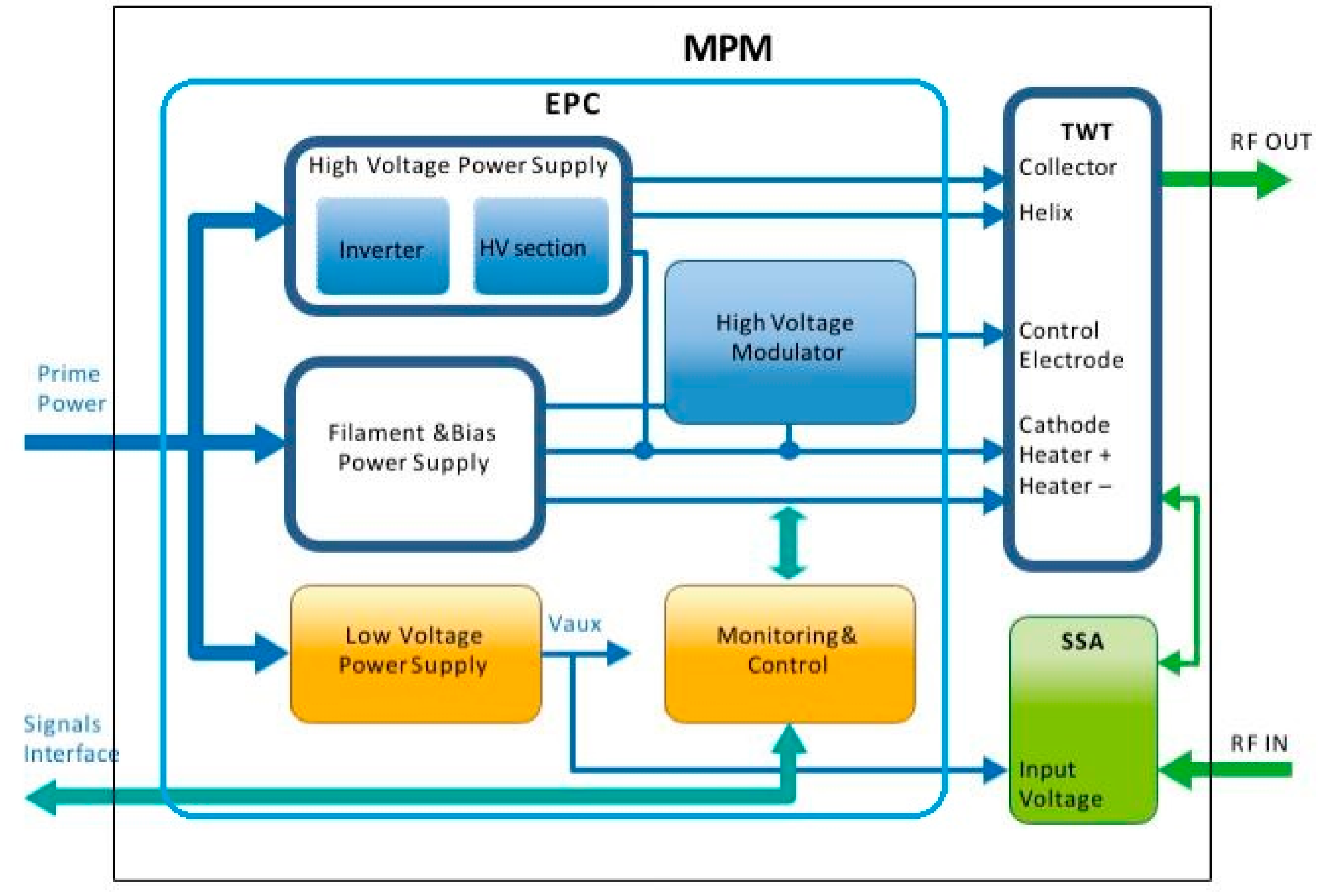
A microwave power module (MPM) is a miniaturized radio frequency power amplifier, combining a low-noise microwave solid-state amplifier (SSA) driver with a medium-power helix traveling-wave tube (TWT) and an electronic power conditioner (EPC), as shown in
Figure 1. MPMs are largely used in many potential system applications, such as commercial and military radar, electronic counter measurements, and airborne platforms [
1,
2]. Progress on MPM developments needs an equalizer combined with a helix TWT to flatten the TWT output gain [
3,
4,
5]. To obtain the advantages of having a broad band, a low voltage standing wave ratio (VSWR), a small size, lightness, and a low cost, a microstrip circuit is most commonly used for the realization of the equalizer [
6,
7,
8,
9]. However, a microstrip equalizer is not tunable and the limits of the equalization curve represent a drawback in the applications. Despite the tuning capacity, a high factor of merit, and low transmission losses, a coaxial equalizer is not largely preferred to a microstrip equalizer due to its large structure, high weight, high cost, narrow band, and high VSWR. Therefore, a smaller, lighter, lower-cost, wider bandwidth, and lower VSWR coaxial solution, compared to the microstrip one, is required for large use of the easily-tunable coaxial equalizer.
In this paper, an optimal design in terms of a low VSWR, being easily-tunable, and having a wide bandwidth, a small size, a low weight, and a low cost for an X-band full coaxial equalizer is presented. The fully-coaxial structure is composed of a coaxial waveguide as the main transmission line and a coaxial cavity loaded with absorbing material as the resonant unit. A sensitivity analysis of the equalizer attenuation amplitude and resonant frequency in terms of the coaxial cavity length, thickness of the absorbing disc, and the insertion depth of the probe are reported. The transmission characteristic curves and the voltage standing wave ratio curves showed a good compromise in terms of the transferred power and adaptive matching impedance at the equalizer input and output ports. With the help of the High-Frequency Structure Simulator HFSS by Ansys, the modeling, simulation, and optimization for an imposed equalizing curve were carried out. The measured results showed that the equalization curve met the requirements well and proved that this optimal structure had the advantage of a large power capacity, a wide operating frequency band, is easily tunable, and good transmission performance.
The paper is organized as follows. In
Section 2, the equalizer structure is analyzed. In
Section 3, the design of the equalizer is presented. In
Section 4, simulations carried out with an HFSS are shown. In
Section 5, a geometric sensitivity analysis of the attenuation amplitude and resonant frequency in terms of the equalizer geometric parameters is reported. The final design simulation results are shown in
Section 6. The measurements are given in
Section 6. Finally, conclusions are discussed in
Section 7.
2. Operating Principle of the Equalizer
Equalizers are devices used to compensate for a negative gain slope in the frequency response of a wide variety of radio frequency (RF) systems. Unlike a standard attenuator with a flat frequency response, an equalizer is a unique kind of attenuator that exhibits a lower insertion loss as frequency increases with some known slope. This is a useful characteristic for system designers working in wideband applications where the gain response of circuit elements or the entire RF chain often varies with frequency. Microwave power amplifiers, such as TWTs, have a high gain near the center operating frequency and a low gain at the band edges. Therefore, to create a flat gain response over the entire operating band, an equalizer with an attenuation curve with the same amplifier dB slope curve as an absolute value must be combined with the amplifier. In
Figure 2, typical input and output curves for a microwave pulse module with a gain equalizer at the output of the driver amplifier and the input of the TWT are shown.
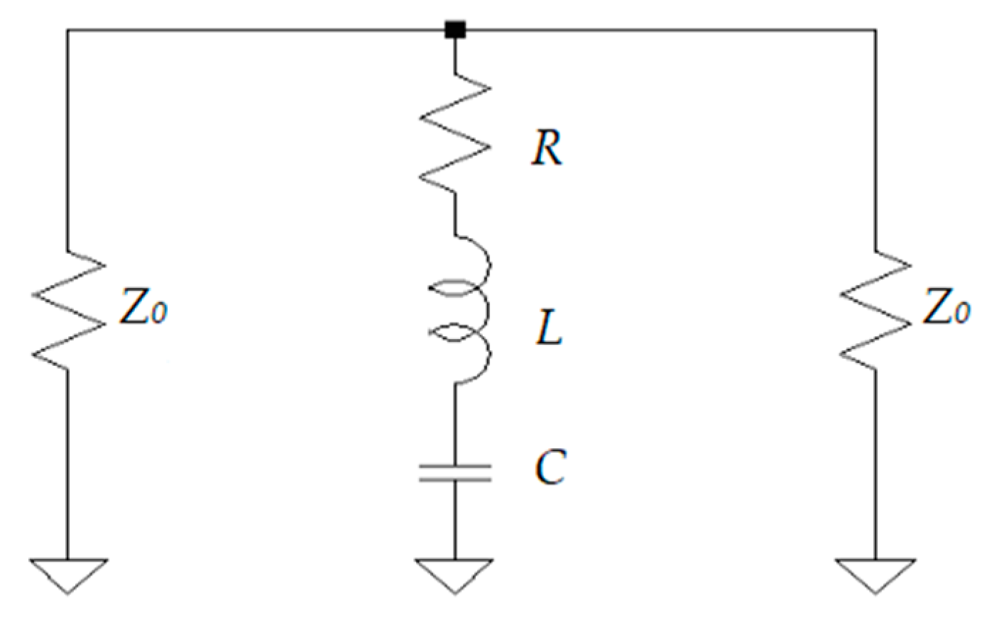
The basic principle of a gain equalizer is based on resonance theory. A simple resonator is composed of a resistance
R, an inductance
L, and a capacitance
C can be used, as shown in
Figure 3.
The resonance frequency and the merit factor of the simple resonator are given by Equations (1) and (2), respectively:
By varying the value of
L and
C, a variation of
occurs. By varying the value of
R, a variation of the merit factor of the circuit
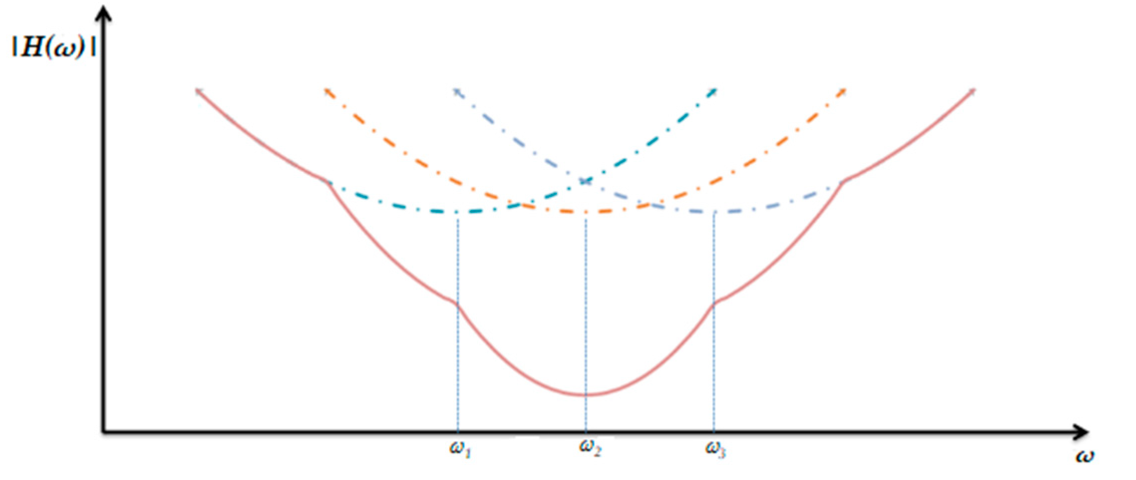
Q occurs, which is related to the maximum attenuation and the width of the curve. By cascading several series of resonators together, each with different, carefully chosen
and
Q values, an equalized response curve that is equal and opposite to the one of the gain amplifier can be obtained. As an example, the transfer function of a three-branch resonator with different
is shown in
Figure 4.
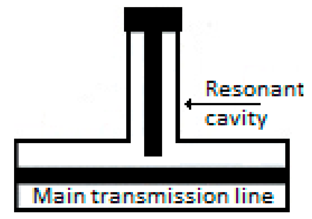
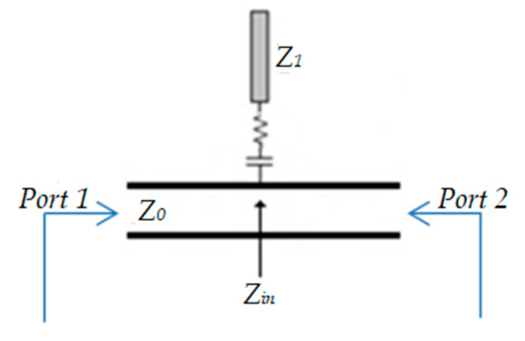
In
Figure 5, a typical microwave coaxial equalizer substructure is shown. It is composed of a coaxial resonant cavity coupled to the main transmission line, which is also coaxial, through a probe in the center of the resonator [
10].
The transmission scattering parameter
S21 of the single coaxial resonator can be calculated using the equivalent circuit shown in
Figure 6, where the capacity
C is related to the coupling structure between the resonant cavity and the main transmission line, which is formed between the main transmission line and the probe, and the resistance
R is produced by the filling material of the resonant cavity, whereas
Z0 and
Z1 are the characteristic impedance of the main transmission line and the resonator branch, respectively.
The impedance
Zin at the input of the resonator branch is given by Equation (3) [
10]:
where
l is the length of the branch and
β is the phase constant.
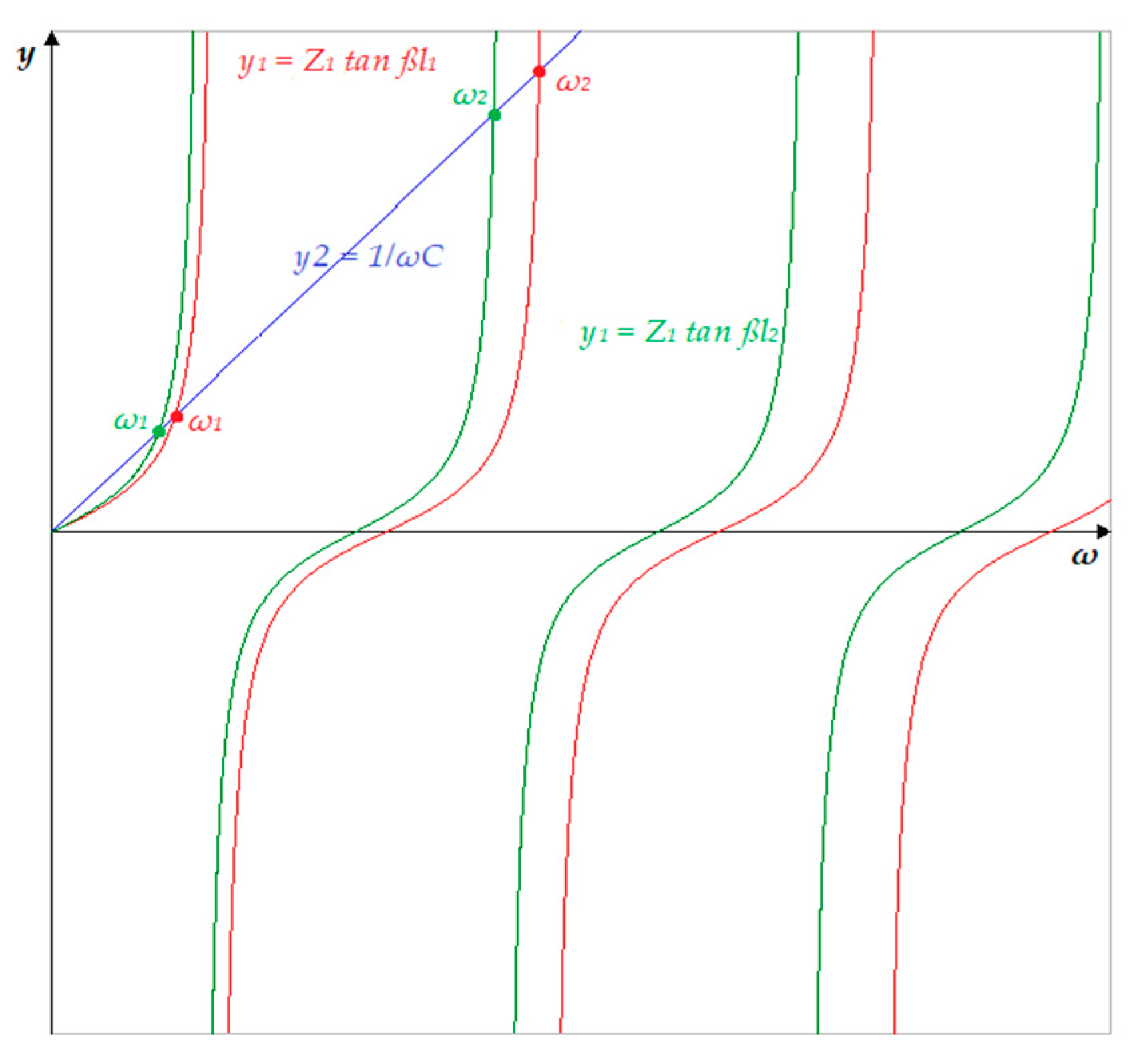
The resonance condition occurs when the following condition is verified:
A graphical representation of the resonance condition is plotted in
Figure 7.
The bandwidth
B of the resonator, given by
varies as a function of the length
l. The lower the length, the wider the bandwidth. By decreasing the length
l, the distance between the
curves increases and bandwidth
B is wider (
Figure 7).
At the resonant frequency, the transmission scattering parameter
S21 is given by Equation (5) [
11]:
3. Design of the Full-Coaxial Equalizer
The microwave amplitude equalizer designed here consists of several substructures formed by absorbent coaxial resonant cavities. Many geometric parameters, such as length and width of the cavity and the probe, the materials, the position of the adjustable metal micrometric screw, the attenuation screw, the number of resonators, etc., have been taken into consideration in the design [
12].
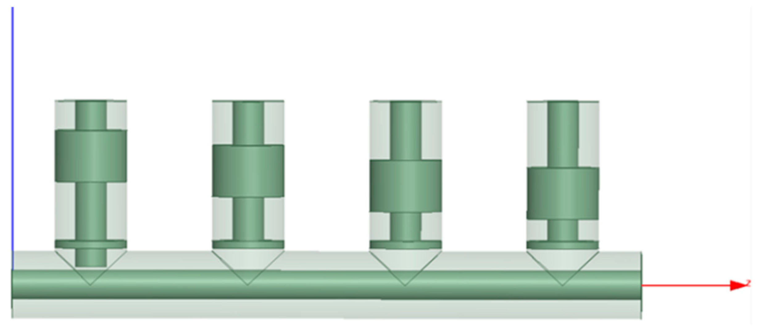
3.1. Description of the Substructure
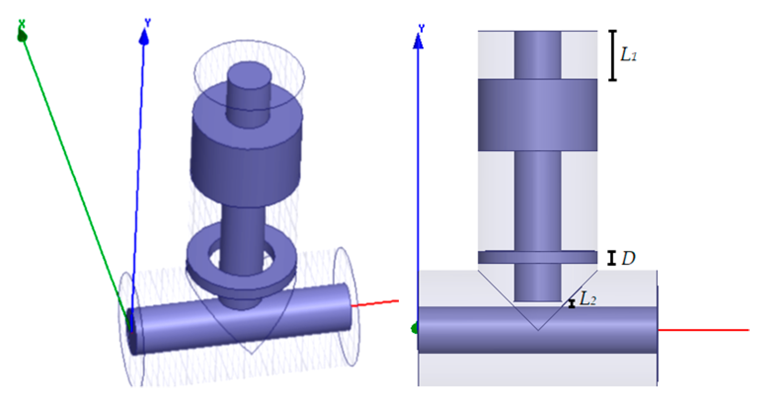
The schematic model of the fully coaxial tunable equalizer is reported in
Figure 8, where
L1 represents the length of the portion of the cavity between the upper edge of the cavity and the upper edge of the tuning piston,
L2 is the insertion depth of the probe, and
D the thickness of the absorbing disc. The greater
L1 is, the shorter the cavity length is.
One end of the resonator is connected to the main transmission line, whereas the other end is short-circuited by an adjustable piston. At the base of the resonator, there is a disk of absorbent material whose thickness determines the merit factor Q of the resonant cavity, and at the same time, has a small effect on the resonance frequency.
The substructure is composed of the following materials:
Brass: for the resonator, as it has excellent conductivity and a low coefficient of thermal expansion.
ECCOSORB
®: for the absorbent disc at the base of the cavity; this is an absorbent material in the microwave region and consists of polyurethane [
13].
Copper: for the main transmission line as it has excellent conductivity and is very ductile such that it can guarantee the desired diameter.
Air: for the rest of the structure.
3.2. Main Transmission Line Size
The value of the characteristic impedance
Z0 of the coaxial line section is given by the following equation:
where
a is the internal diameter of the external conductor,
b is the external diameter of the internal conductor, and
is the electrical constant of the insulating material.
If = 1 (in the case of air), the characteristic impedance value is equal to 50 Ω for b/a = 2.3 approximately. For the proposed equalizer, the internal transmission line is made of copper, whereas the external part is air. The radius values for the internal conductor and of the external cylinder are 1 mm and 2.3 mm, respectively.
3.3. Length of the Resonator
The length l of the coaxial resonator l is determined by Equation (7):
where λ
o is the resonance wavelength.
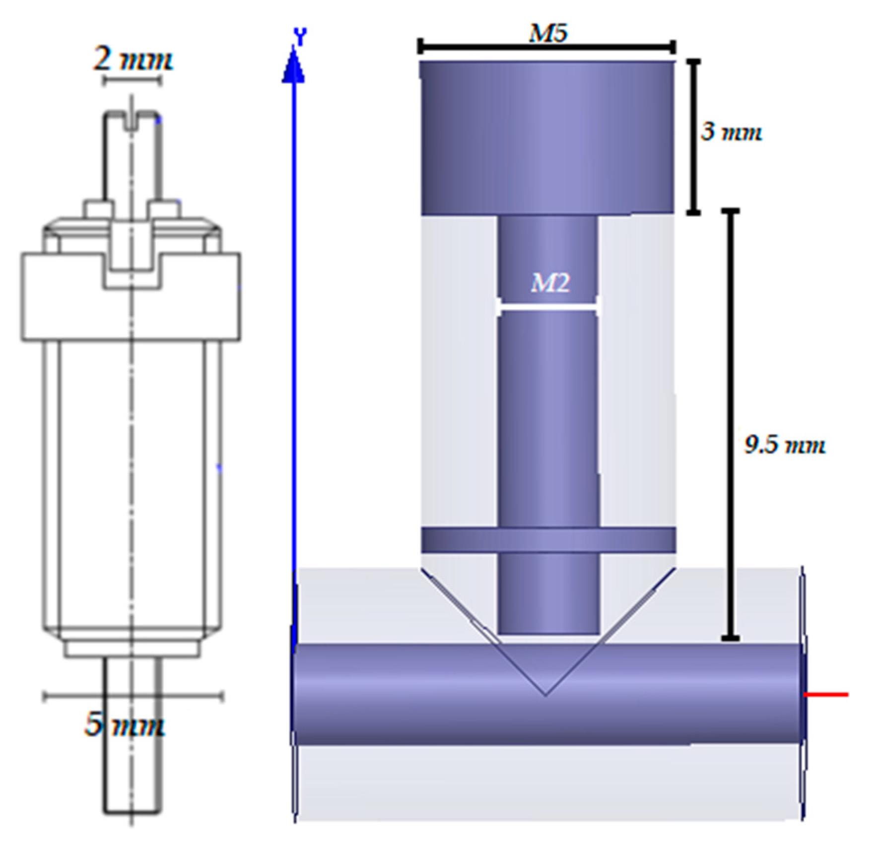
Starting from Equation (7) and by considering that the edges of the operating band are 8 and 12 GHz, it is possible to obtain the length of the cavity, which in the worst case will be 9.5 mm.
3.4. Cavity and Probe Diameters
Two tuning screws are present in the resonant cavity. The first has a larger diameter, which allows for adjusting the length of the cavity, while the second has a smaller diameter and is in the center of the first, which allows for adjusting the coupling with the main transmission line.
Regarding the dimensions of the diameters of the resonant cavity and the probe, the main factors to take into account are the maximum power capacity, the dissipation of the conductor, the matching impedance, and the propagation of the Transverse Electro-Magnetic TEM mode.
For the proposed equalizer, according to the relationship of the characteristic impedance, an external diameter of 4.6 mm for the cavity and an internal diameter of 2.3 mm for the probe were chosen. Based on these measurements, an M5 thread (International Organization for Standardization ISO standard in terms of threads), which corresponds to a diameter of 5 mm as the external diameter of the cavity, and an M2 thread, which corresponds to a diameter of 2 mm for the probe, were chosen, as reported in
Figure 9.
3.5. Absorbing Disc Thickness
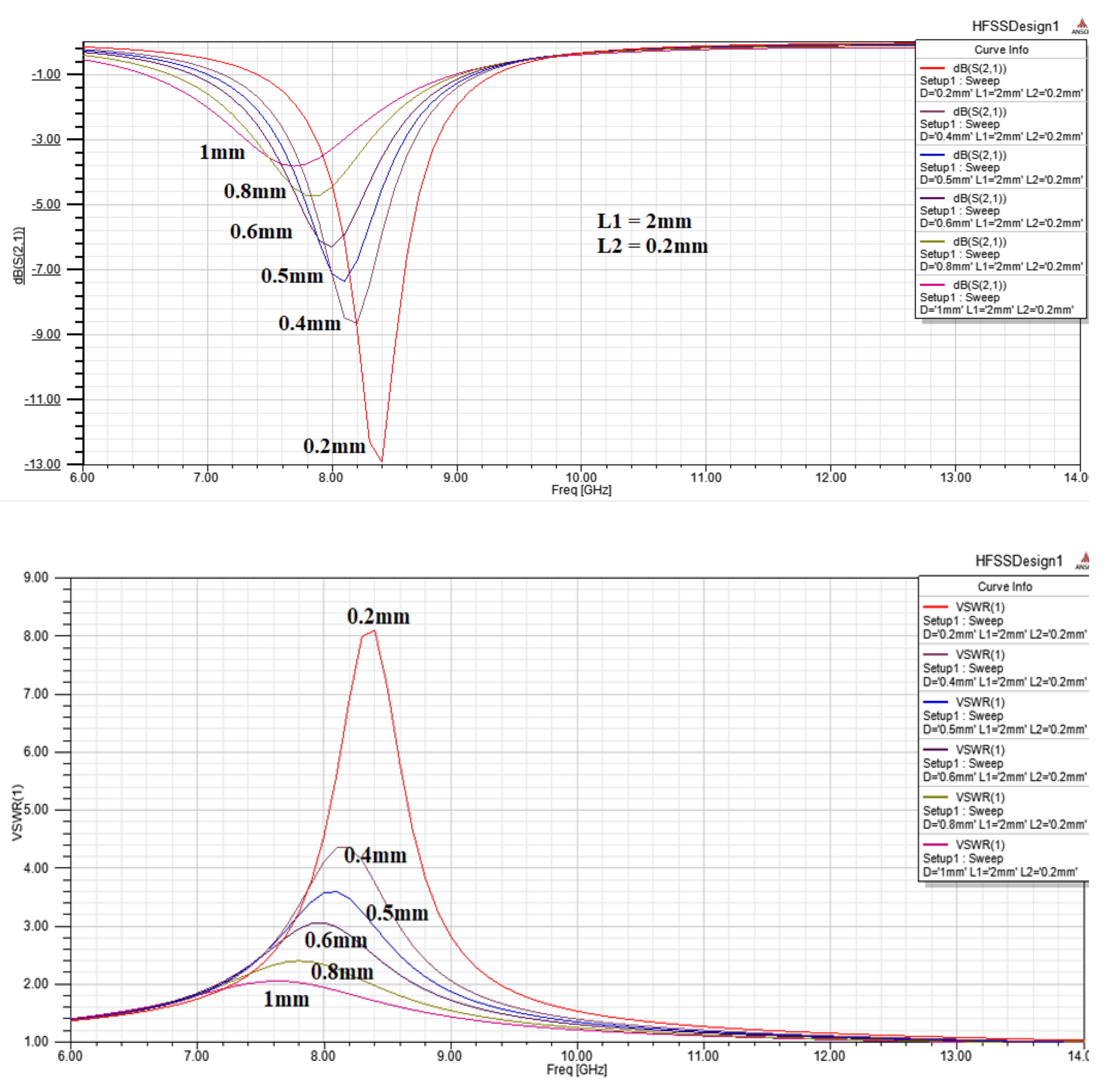
The thickness of the absorbing disc D is directly related to the thickness of the resonator resistance, where increasing the absorbing disc thickness increases the resistance R, and according to Equation (2), decreases Q.
By keeping the length of the cavity
L1 and the insertion depth of the probe
L2 constant, the transmission coefficient
S21 and the input VSWR curves vs. frequency with the thickness of the absorption cylinder as a parameter are plotted in
Figure 10. It can be observed that the thicker the absorption cylinder, the lower the resonance frequency and the attenuation, with a lower input VSWR.
The role of the absorbent disc in the ECCOSORB® is to reduce the VSWR and eliminate the transmission characteristic of each substructure. The greater the thickness of the absorbent disc, the lower the merit factor Q of the resonator, and therefore the lower the maximum achievable attenuation. Meanwhile, this allows for covering a greater frequency range with a single substructure, and consequently, by using only a few resonators, it is possible to cover the entire 8–12 GHz interest band while obtaining a more compact equalizer. To have a lower VSWR, it would be sufficient to increase the thickness of the absorbent disc.
A disk thickness of 1 mm as a good compromise between S21 and VSWR was chosen.
3.6. Number of Substructures
The number of secondary structures that must be interconnected to the mainline depends on the Q value of the single substructure, the maximum attenuation range that each of them can provide, the frequency band to be equalized, and the degree of precision required when adjusting the curve. For the proposed equalizer, a four-stub substructure was designed. For a thickness of ECCOSORB® equal to 1 mm and by verifying that the maximum value of attenuation that each substructure can give is about 4 dB, the waveform to be given at the input of the amplifier may be equalized in a fairly accurate and precise way. The distance between two adjacent stubs, from the center of a cavity to the center of the next cavity, was equal to 10 mm. This value corresponds to the minimum possible distance, as indicated by the mechanical designer, to obtain a compact structure. The drilling of the aluminum structure, to be threaded to insert the tuning screws, must not create a wall thickness that is too thin between a cavity and the adjacent one, which could collapse as a result of subsequent mechanical processing. At this distance value, the contribution of each substructure is not influenced by that of the adjacent substructures, as verified using simulations.
4. Simulations
In
Figure 11, the schematic model design of the proposed equalizer using four coaxial cascaded cavity resonators is given.
The equalizer was designed to match the gain amplifier curve with the gain attenuation curve at each working frequency.
Figure 12 shows the attenuation curves of the designed equalizer, which consisted of the sum of the individual attenuation curves of each substructure.
Starting from the structure shown in
Figure 11 and with the help of HFSS by Ansoft, it was possible to model and simulate a single resonator by disconnecting all the others.
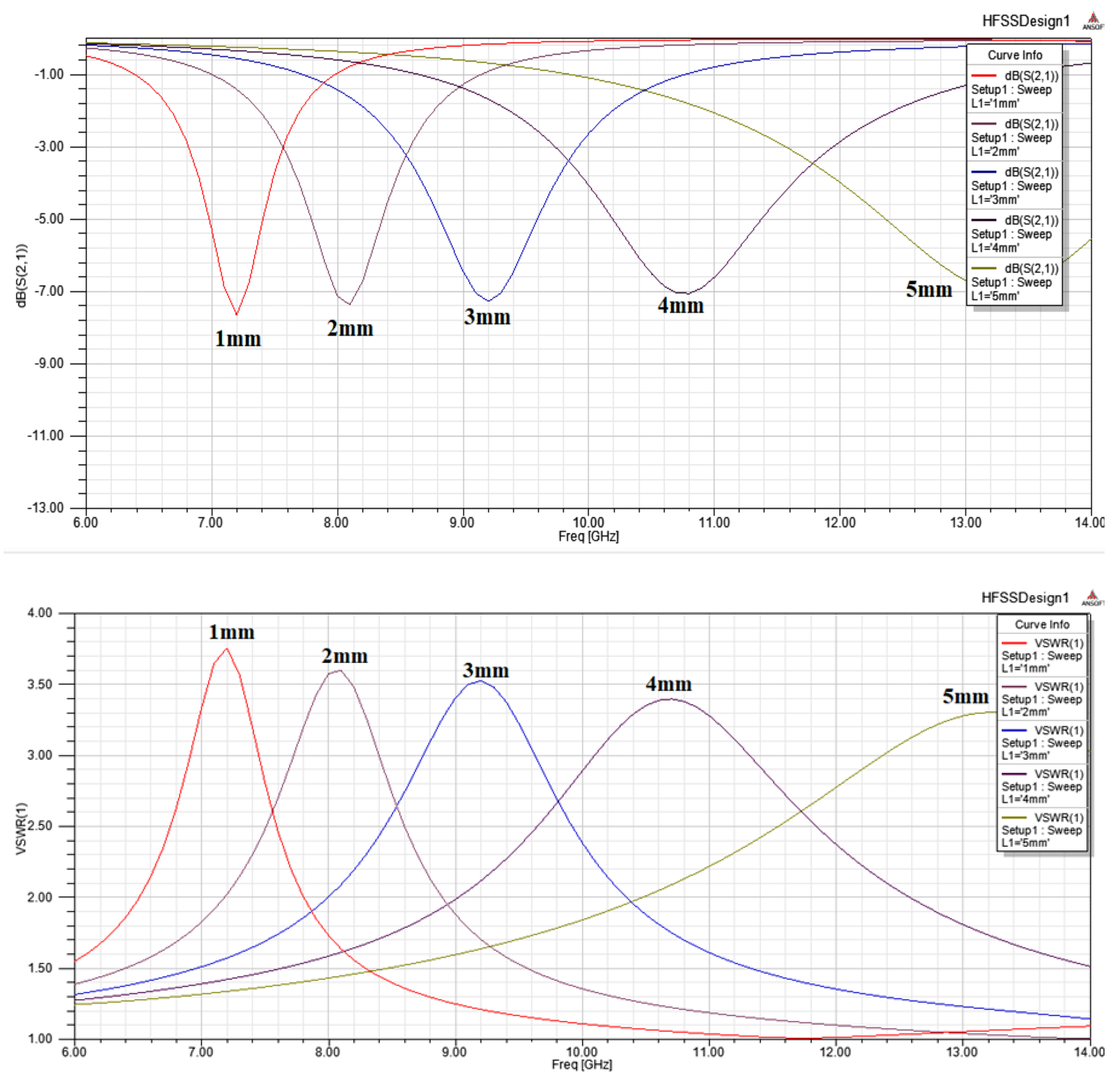
The behaviors of the magnitude transmission coefficient
S21 and VSWR vs. frequency were simulated by keeping the
L2 insertion depth of the probe and the
D thickness of the absorbing disc constant while the
L1 length of the portion of the cavity between the upper edge of the cavity and the upper edge of the tuning piston was used as a parameter. The results of the simulations of the magnitude
S21 and the VSWR with constant values of
L2 = 0.2 mm and
D = 0.5 mm, and by varying the position of the adjustable micrometric cylinder from 1 to 5 mm (with a pitch of 1 mm) at the upper end or by adjusting the length of the resonator cavity, are shown in
Figure 13.
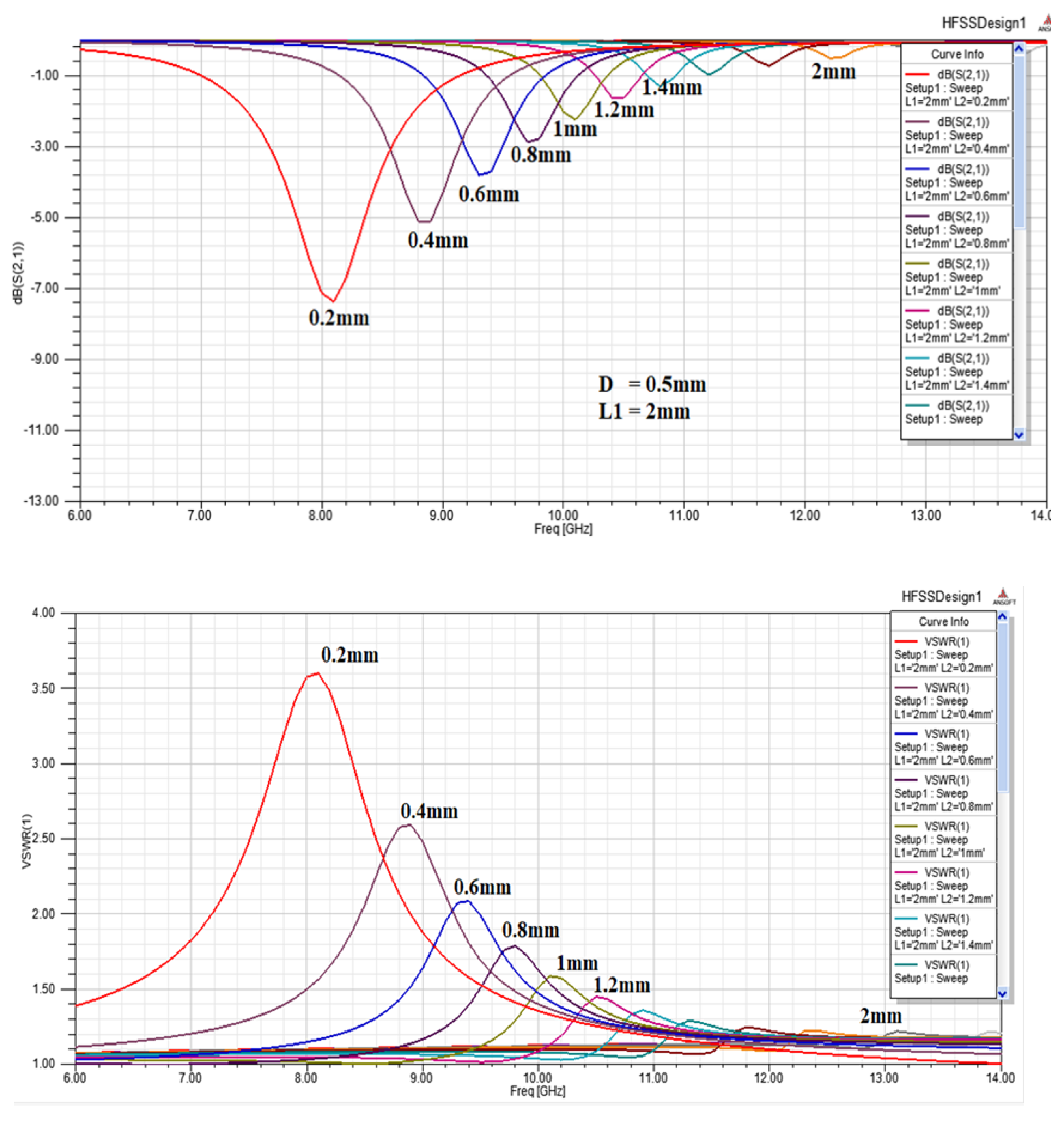
Moreover, the behaviors of the magnitude transmission coefficient S21 and VSWR vs. frequency were simulated by maintaining the L1 length of the portion of the cavity between the upper edge of the cavity and the upper edge of the tuning piston and the D thickness of the absorbing disc constant while the L2 insertion depth of the probe was used as a parameter.
The results of the simulations of the magnitude of
S21 and the VSWR vs. frequency with
L1 = 2 mm (from the upper end of the structure) and
D = 0.5 mm, with a varying position of the screw inside the cylinder or adjusting the depth of the probe coupled with the main transmission line, are shown in
Figure 13.
The adjustment of the depth of the coupled probe changed the resonant frequency and the attenuation due to the change of the coupling capacity between the resonator and the main transmission line.
Figure 14 shows that the deeper the probe was inserted, the lower the resonant frequency and the greater the attenuation, and at the same time, the VSWR was increased.
If the absorbent disc was positioned at the point where the intensity of the magnetic field was greater than the strength of the electric field, the resonant frequency decreased to a lower value; therefore, keeping its position constant avoids a further adjustment parameter.
Figure 13 and
Figure 14 show that the lower the length of the cavity, the higher the resonance frequency and the lower the attenuation. At the same time, with the reduced cavity length, the input VSWR was decreased.
By adjusting the length of the cavity (adjustable piston) and the coupling of the screw at the center of the cavity with the main transmission line (also adjustable), then changing the parameters L1 and L2, respectively, and fixing the thickness of the absorbent disc a priori, any signal over the 8–12 GHz frequency range could be attenuated.
The adjustment of the piston and the tuning screw does not need to be done before mounting the equalizer to the rest of the system, but this can be done after connecting the driver to the input of the equalizer and the TWT to its output. In this way, it is possible to adjust, in a fairly fine way, the desired attenuation according to the specific application, and therefore no further compensation will be necessary, which might be the case for an equalizer with fixed parameters.
The simulated data showed an optimal equalizer design. The curves showed a good compromise in terms of the transferred power and the adaptive matching impedance at the input and output ports.
5. Geometric Sensitivity Analysis
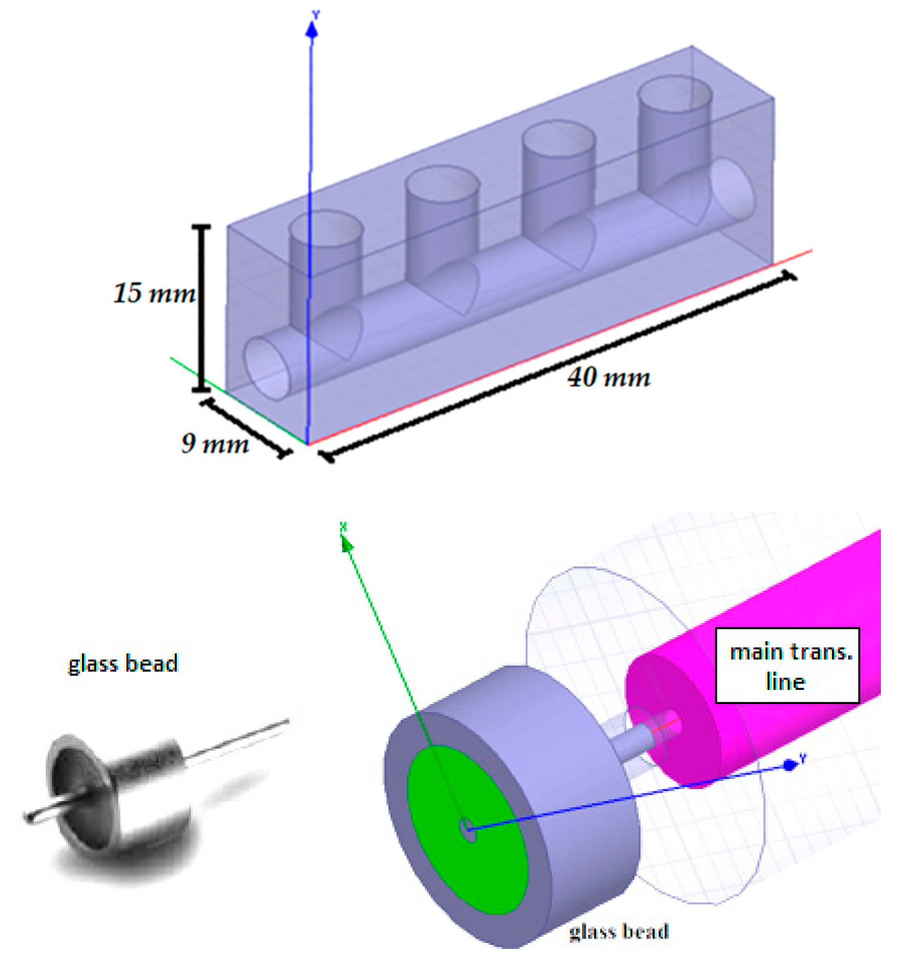
The external design of the device is shown in
Figure 15. It had a height, a width, and a depth of 15 mm, 9 mm, and 40 mm, respectively. It was created by perforating an aluminum parallelepiped and inserting the tuning screws and the absorption disc into it. The main transmission line was interfaced with the outside through glass beads.
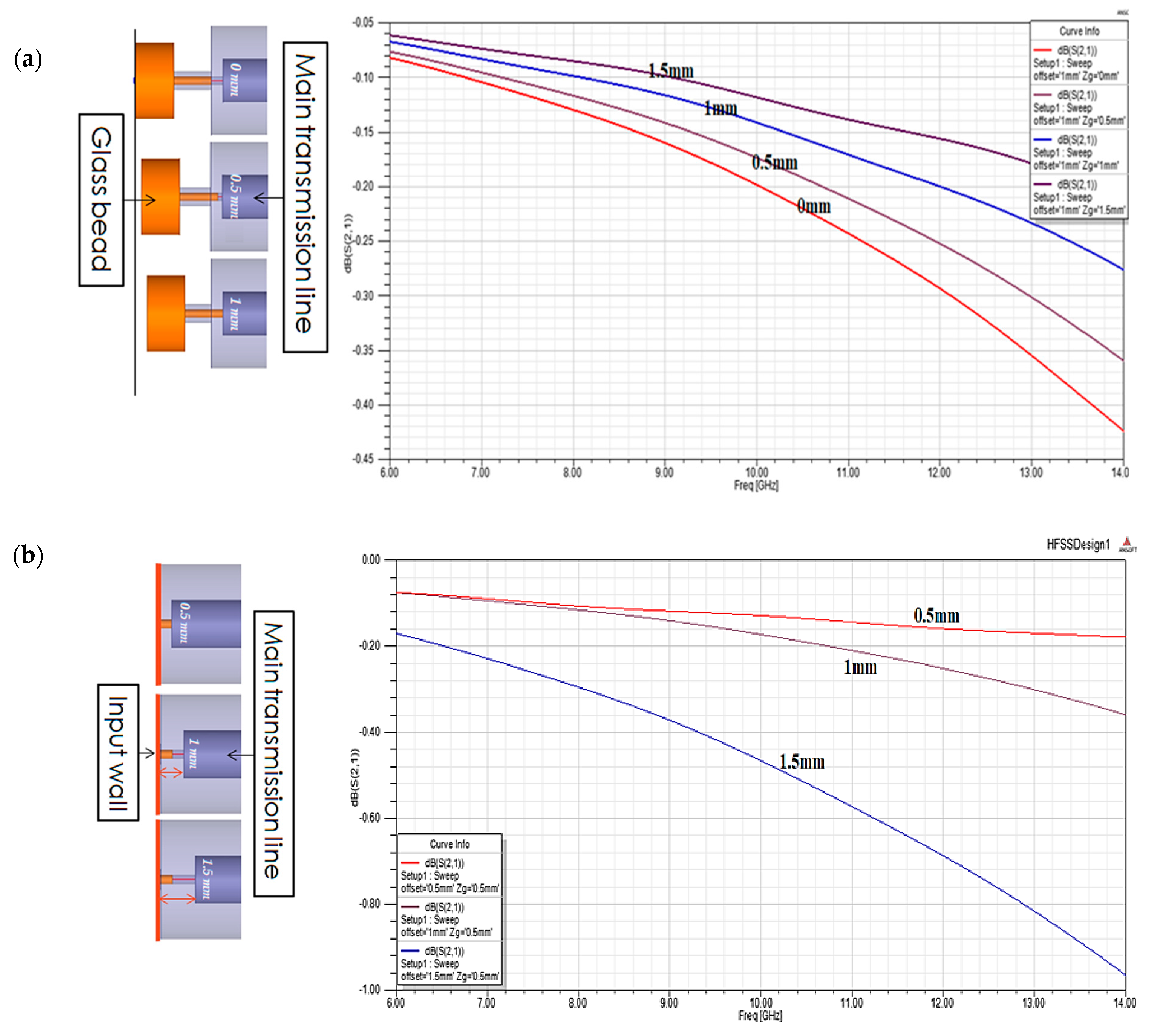
A sensitivity analysis of the insertion of the glass bead into the structure and of the distance of the main transmission line between the input and output ports was carried out with HFSS.
The insertion of the glass bead and the distance of the main transmission line from the input and output wall were not among the electronic design parameters as they were parameters that concern the mechanical design. However, they played a fundamental role in the project. By changing the insertion length of the glass bead in the structure and the distance of the main copper line from the input and output walls, the transmission coefficient changed, and consequently, the power transferred from the previous stage to the next stage also changed. The results of the simulation of the sensitivity analysis are reported in
Figure 16.
Figure 16a shows the more the glass bead was inserted into the structure, the lower the attenuation.
Figure 16b shows the greater the distance of the main transmission line between the input and output port, the greater the mismatch.
6. Final Equalizer Simulation Results
In
Table 1, the final design parameters of the optimized four-stub equalizer are reported.
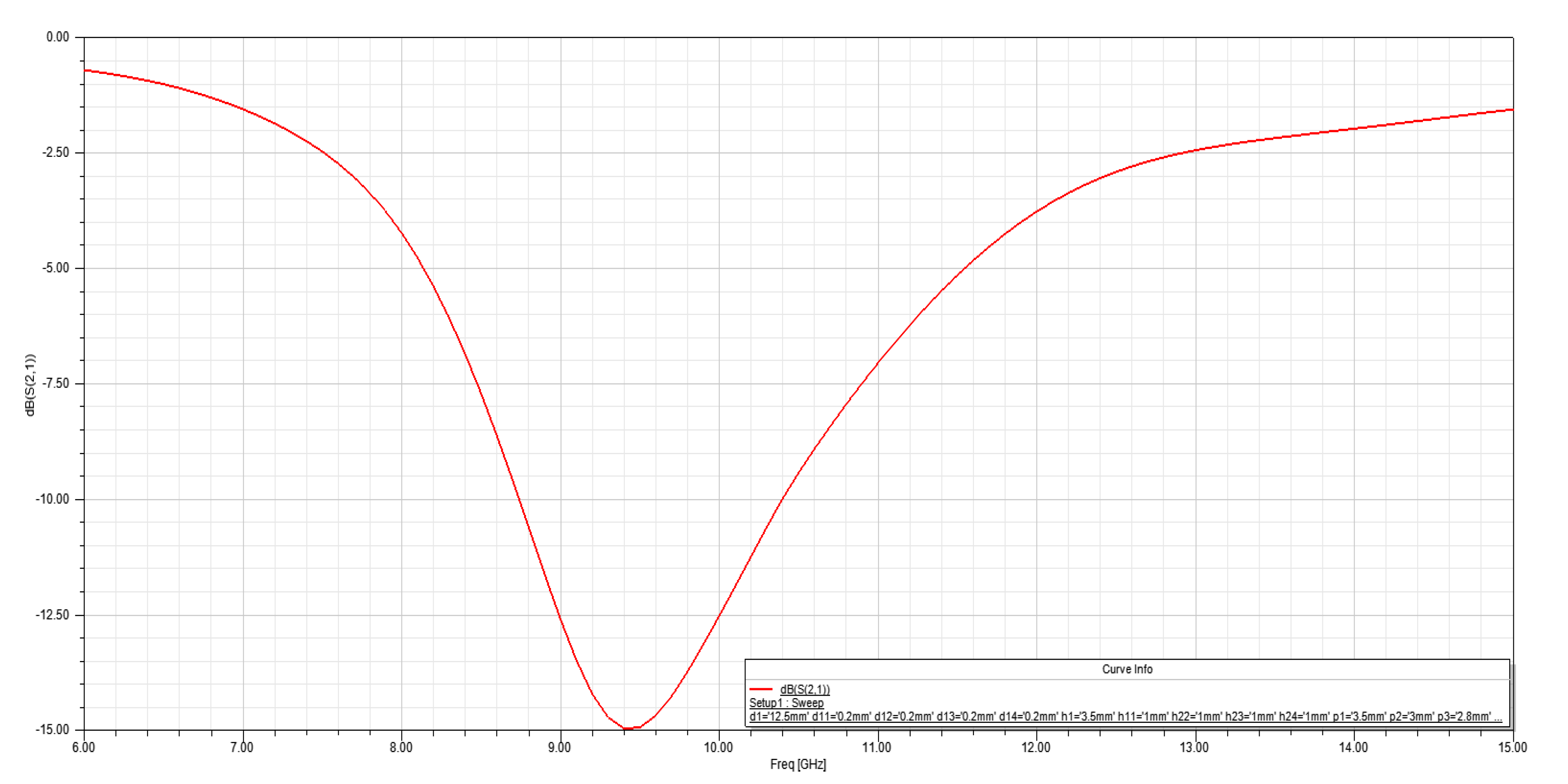
In
Figure 17, the simulated equalizer transmission results vs. frequency, obtained with the final design parameters, are shown. The curve met the required waveform needed to compensate for the TWT gain slope.
In
Figure 18, the results of the simulation for the input and output equalizer VSWR curves are shown.
To keep the VSWR low, a not-too-thin absorbent disc or a not-too-coupled probe needed to be used. In both cases, this led to a decrease in attenuation. Since the desired attenuation was lower than what was simulated, this trade-off can easily be solved. For the input VSWR, a good simulated low-value of 2.2 was obtained.
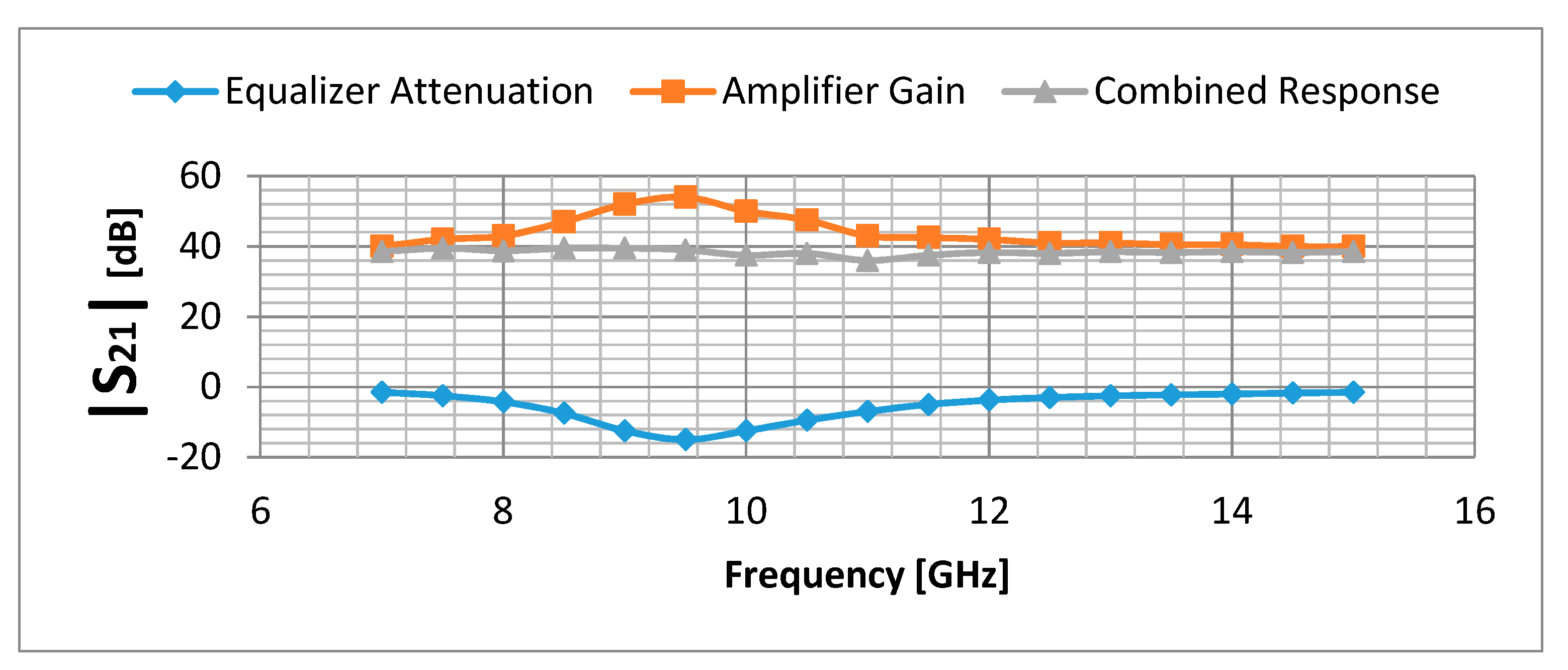
7. Measurement Results
The X-band, fully-coaxial, broadband, easily-tunable equalizer was designed and fabricated. Measured data of the equalizer attenuation and amplifier gain over the entire operating X-band are shown in
Figure 19.
The equalizer operating at the X-band presented a transmission curve over the entire frequency band, which when combined with the TWT gain curve, gave a flat gain response.
8. Conclusions
The simulation, design, and experimental demonstration of an X-band, fully-coaxial, broadband, easily-tunable equalizer for radar applications was presented. The structure, only 40 × 15 × 9 mm3 in size, has the advantage of small size, large power capacity, wide operating frequency band, convenient tuning, and good transmission performance. Finally, the measured attenuation curve of the equalizer showed an optimal combined response waveform with the measured TWT gain curve confirming the quality of the proposed design.
By comparing the designed equalizer to the microstrip equalizer, when connected to the TWT in an MPM, the designed equalizer ensures a low coupling loss, in addition to the advantage of being able to be tuned at different frequencies without the need to redesign the device. Compared to similar coaxial equalizers, the designed equalizer, thanks to the absorbent disc composed of an innovative material, allows for obtaining attenuation curves for each resonator that cover a greater frequency range. Therefore, using just a few substructures, it is possible to cover the entire predetermined frequency range. This allows for producing a compact device that is easy to use where dimensions for radar applications are a critical requirement, and it is easy to tune to different desired frequencies according to applications.


