1. Introduction
Field Programmable Gate Arrays (FPGAs) revolutionized the field of embedded systems by providing the flexibility of reconfiguration in real time. FPGAs are considered to be a cost-effective replacement for ASICs in many applications as they provide benefits for users on two fronts: time and cost. First, they provide users with the flexibility to replace or amend their logic in the field, reducing the lengthy time involved in the process of ASIC manufacturing and development. Secondly, the cost incurred in the procurement of FPGAs is much less than developing an ASIC from scratch. However, the fact that state-of-the-art SRAM-based FPGAs are fabricated in the latest technology nodes, for example, Xilinx UltraScale+ in a 14 nm FinFET node, means that this class of semiconductor devices are vulnerable to radiation-induced failures, aging and electro-migration issues to name a few. Therefore, FPGAs also pose a challenge with respect to safety and security in mission-critical application areas and government/military sectors respectively; where the need for a reliable system is a must.
However, even these vulnerabilities have not hindered the widespread adoption of FPGAs in safety-critical fields such as avionics, aerospace, automotive, biomedical, financial and cryptographic systems where high reliability, high availability and high assurance are critical requirements. Systems, targeting these application domains are rigorously designed to achieve the required level of hardness-assurance according to industrial standards, for example, ISO26262 [
1]. Vendors, also continuously spin-off design tools and methodologies to address the market needs for safety-critical domains. Information security standards for cryptographic modules or devices such as ISO27001 [
2] and FIPS 140-2 [
3] promote the idea of implementing well-defined, physically and logically separated data paths for information exchange on black (enciphered data) and red lines (plain data). The IDF itself is a part of the certified Xilinx IEC61508 toolchain [
4]. IDF, in particular, achieves better system-level fault tolerance due to the module-level fault containment approach. For this purpose, it maps the logical interconnections of modules in a way that its physical level floor-planning on-chip avoids Single Point of Failures (SPOFs) which can make redundancy-based approaches such as Duplication With Comparison (DWC) and Triple Modular Redundancy (TMR) useless. Until now, designers for this market segment relied on multi-chip solutions for fault containment but the increased logic density and the industry-shift to processor-integrated FPGA fabrics, such as ZynQ SoCs demand on-chip isolation solutions.
To assess the effectiveness of the IDF, fault injection is needed to ensure that Single Point of Failures (SPOFs) are indeed avoided. Due to strict layout constraints imposed by IDF, use of Internal Configuration Access Port (ICAP) located in the Programmable Logic (PL) part of ZynQ, is not a good option as it can make isolation difficult to achieve. Therefore, fault injection has to be done over the Processor Configuration Access Port (PCAP) located in the Programmable System (PS) part of ZynQ. To the best of our knowledge, Xilinx does not provide any built-in EDA tools or library for frame-level fault injection over the PCAP interface as compared to AXI-ICAP. Therefore, existing fault injection methodologies for PCAP such as [
5,
6,
7] require a large reconfiguration time and are thus slow. Furthermore, previous works that utilize PCAP rely on full bit-stream for fault injection purposes that have significant memory overhead. This paper introduces a testing and evaluation methodology for IDF designs that overcomes those limitations. This is achieved by reverse-engineering the partial bit-stream format for error injection so that full reconfiguration is not needed. To do so, a Partial Bit-stream Frame Template (PFT) is developed to enable run-time partial bit-stream generation and bit-flips inside DRAM memory. Then, the modified PFT is written back to the configuration memory using PCAP.
The proposed methodology was tested on a Xilinx ZynQ SoC housing an AES-based DWC Design Under Test (DUT) in the programmable logic portion. The DUT is carefully floor-planned with the strongest layout requirements of IDF with the overall goal of minimizing cross-domain errors or common mode failures. The results show that the proposed PFT-based methodology allows for much faster fault injections in comparison to existing schemes.
The paper is structured in the following manner:
Section 1 provides the introduction and the motivation for the research,
Section 2 covers the related work and background needed to follow the rest of the paper,
Section 3 discusses the proposed methodology and
Section 4 evaluates the methodology using a case study. Finally,
Section 5 concludes the paper and provides some ideas for future work.
2. Background and Related Work
When creating an FPGA- or SoC-based design, the fundamental performance metrics for the designer have traditionally been area, time, and power. These constraints are what limit the implementation or impact of the cost in many systems. However, in order to create a robust and dependable design, there are other aspects that must be considered as well. In the following, other considerations that must be taken care of when developing reliable and dependable systems are summarized.
Security: Design security is a critical need in many industries, and classified and non-classified military applications. For this purpose, data encryption techniques are being used to mask actual data from the adversary. However, with the emergence of Side Channel Attacks (SCAs), researchers proposed and evaluated several designs, exposing their weaknesses. For example Lumbiarres et al. [
8] created a method for achieving data security termed as “Faking countermeasure”. Their proposed solution is processing the unencrypted or plain-text data with the help of a false/fake key whose Electromagnetic (EM) wave emissions will mislead the attacker. The False key used for the purpose holds the KFALSE = KREAL ⨁ KMASK relationship with the original key. The additional operation needed at the end of each mix-column operation is exclusive-or of the false output with KREAL. This process adds a huge overhead for large chunks of data, with a primary focus on the AES design and thus cannot be extended to other cipher schemes. In the past, the National Security Agency (NSA) worked with Xilinx to secure Virtex-4 against attacks mentioned in [
9]. The work performed was focused on evaluating isolation of basic building blocks on an FPGA; CLB’s and Global switch matrix (GSM) which is used to facilitate interconnect between CLB to CLB. The idea of a Fence; to provide a physical isolation was introduced in this paper. Xilinx further improved on this idea to create the IDF [
10,
11].
Reconfiguration: With the invention of dynamic partial reconfiguration (DPR), many applications can now share the same FPGA chip, carrying out their desired operations, side by side. DPR also opened doors to an entire new threat model, originally not present in traditional FPGAs. Zao et al. showed that side channel attacks on such environment are possible by using ring oscillators (RO), placing them in close proximity to secondary user’s space with the sole purpose of snooping data and information gathering/leaking [
12]. Their RO based design acts as a power monitoring device which can relay information such as switching of bit(s) from 0 to 1 which can then be monitored to build a dictionary model upon which co-relation can be applied to extract the actual data. Moreover, such a design can be placed without using place and route constraints. Hence isolation (between users sharing the same FPGA space) to prevent Side Channel Attacks (SCA) is necessary.
Reconfiguration enabled FPGAs to gain a massive acceptance for big data analytics and parallel and distributed computational systems. Many companies employ solutions comprising an FPGA that can hold multi-tenants in cloud computing; as their general purpose computation machine. DPR is one of the key requirements to enable this form of cloud computing. DPR allows users to time multiplex FPGA resources enabling effective use of chip logic density. The reconfiguration time was thus reduced as the partial bit-stream size is fairly smaller than the whole bit-stream [
13]. DPR allows a user design to be placed in static and dynamic parts. The dynamic or partial reconfigurable module can be arranged on chip in various configurations namely island style, slot style and grid style [
14]. Each style has its own pros and cons. The island style is the simplest to implement but suffers from internal fragmentation resulting in a high percentage of resource wastage. Slot style configuration does not have fragmentation problems where a module can occupy resources as per its needs. Tiling of Reconfiguration Module (RM) region is a very complex task in which one has to keep in mind the placement of routes and their cross-over from static to dynamic regions. Thus, the DPR style to use depends on the user requirements and may vary from application to application. It may also consist of a model that is hybrid combining two or more styles.
Single Point of Failure (SPOF) Prevention: Embedded systems are designed and deployed every day to be used in every aspect of life ranging from submarines to handheld smart phones. If proper fault isolation and control mechanisms are not kept in mind during the design, the damages could be catastrophic as safety-critical systems are designed with the ultimate goal of being reliable. To avoid SPOF in systems, various solutions were provided. SPOF prevention can be put in place at (a) Internal components level (b) System level (Distributed Systems) (c) or a site wide level (Repetition). In the work provided in [
15], SPOF prevention is introduced by building upon the existing Triple Module Redundancy (TMR) methods. In Reference [
15], the authors propose the use of minority voters along with the majority voters to detect faults with better granularity. This technique can detect and help the user in correcting the fault by using the output of minority voters as a flag. Should the system fail to correct/detect the SPOF, it can minimize the damages if only the system is implemented upon isolated model; preferably at both physical and logical levels.
Heterogeneity: The first FPGAs developed were homogeneous devices. Presently, various functionalities are bundled down on a single chip. Isolated design helps achieve the best of FPGA heterogeneous nature, where a user can access and explore DSPs, BRAMs, and CLBs all in one place. In a heterogeneous system on chip (HRSoC) devices, user applications can be easily divided into various tasks. They can be either hardware accelerators-based which are built-into devices at pre-defined partition(s) or locations or can be implemented as a software task based on computing elements or CLBs. Gantel et al. in [
16] made use of the heterogeneous nature of FPGA along with isolation to combine flexibility and reliability. Gantel used two isolated partitions (separately) that are identical to each other (resource wise) to ensure that the relocation process is achievable without physically damaging the chip (just as in IDF trusted routes are established to communicate various modules of a partition). A signal that is sink to two or more modules is split into different signals and passed through LUT resources to form trusted routes. Use of hard macros such as
where ‘i, j’ are the valid XY coordinates of the chip, is done to constraint the synthesizer to a valid and desirable position. The isolation of designs ensured the error free relocation of modules in accessible dynamic partition space.
Fault Tolerance: The ability to control and withstand system failures is always a desired feature and is a requirement in government cryptographic systems, avionics, and functional safety electronics. This can be achieved by combining several systems that operate in parallel to ensure that the failure of some of them would not cause a global failure. This was proposed in [
17], “A system composed of two or more redundant subsystems connected in parallel fashion, has a failure probability which is equals to the multiplicative product of the probabilities of each of the subsystems failing”. i.e., If the subsystems both had failure probability of
, then the system made up of these subsystems has a reduced failure probability of
=
, which is many degrees lower in magnitude than individual subsystem failure rate [
17]. However, this calculation assumes that probabilities of failure on each module are independent in nature i.e., the subsystems do not have a SPOF or common failure mode. This notion is the genesis of the isolation design flow. Fault-tolerance (FT) can be achieved by configuration scrubbing, floor-planning, module decomposition, reduced functionality modes, built-in self-tests (BIT) fault containment, failover and failback, redundant alarms, configuration memory error detection and error-recovery or correction mechanisms. Validation and verification of such FT methods can be realized using automated test procedures, diagnostic logging, design for test, and formal verification.
Xilinx Isolation Design Flow: Incorporating IDF in a user design has several advantages, such as; (1) IDF provides physical isolation between various modules, placed on a single-chip. (2) IDF helps in restricting error propagation between modules in an event of failure. (3) IDF allows ease of debugging and identification of the module causing a fault in an event of failure. (4) IDF allows enhanced failure protection by the use of trusting routing and well-defined logical boundary and separation of the modules. Although the advantages that IDF provides are important, it also has the following drawbacks: (1), IDF rules can be difficult to comprehend for novice users as sometime, they require FPGA placement and routing information that normal users may not possess. (2) IDF essentially limits users to design in a constrained environment (area wise) so larger designs might be difficult to fit onto chip along with IDF and lastly, incorporating IDF in a design, restricts the usage of dynamic partial reconfiguration once enabled. If a user wishes to implement IDF and DPR, side by side he has to do it with the help of third-party tools and API such as Go-Ahead [
18] and BITMAN [
19].
From this literature review, it is clear that modular isolation has many beneficial use cases. Many applications demand that the system works flawlessly, with an extreme degree of reliability. However, to verify that IDF is effective in avoiding or reducing SPOFs fault injection is needed. Current methodologies such as in [
5,
6,
7,
13,
20] use PCAP to to emulate errors by placing ready-made partial bit-streams in an SD card to inject the errors. This results in a large injection time.
Other FI methods such as [
21,
22] make use of JTAG and ICAP interface respectively, to inject faults in DUT using external hardware whereas our proposed technique does not require any additional hardware to inject faults. Moreover, [
21,
22] also requires modification in DUT, such as insertion of
Data Generator, Fault Generator, Error-detection, JTAG BSCAN modules and usage of external PCB hardware in order to emulate successful SEUs. Tobias et al. in [
23] proposed usage of Soft-core processor in combination with ICAP, to inject and mitigate faults within 0.82 ms of its generation at the overhead of 32 KiB MicroBlaze memory. However, using a soft-core processor not only incurs a toll on PL resources (routing and logic) but may lead to other side-effects suggested by Villalta et al. in [
5,
24]. Author’s stresses that using ICAP for FI might be precarious and could easily lead to injection side-effects if a configuration bit that belongs to logic controlling ICAP is flipped and thus discourages the use of ICAP interface for FI.
In the following, a methodology that significantly accelerates fault injection is presented and evaluated on a single chip cryptographic application i.e., AES core mapped onto a ZynQ SoC.Proposed methodology uses PCAP for non-intrusive FI, saving precious PL resources and additional PCB hardware or OCD tool [
25] in comparison to existing methodologies in [
21,
22,
23].
4. Evaluation
This section evaluates the proposed methodology using a single-chip cryptography application as a case study. Specifically, an Advanced Encryption Standard (AES) Duplication With Comparison (DWC) design is used.
Xilinx provided IDF comes in two flavors: (1) IDF for Plan-ahead and (2) IDF for Vivado. The rules and key concepts of IDF defined for both do not vary, but the approach for its use and isolation verification method varies significantly i.e., IVT for (1) and VIV for (2) respectively. We chose to work with Vivado’s IDF because the other tool has become obsolete. For this purpose, a design has been implemented on Zynq SoC, “Zed-Board” that conforms to the rules specified by the IDF. The verification of all IDF Design Rule Checks (DRCs) were performed using the Vivado’s Isolation Verifier (VIV) to qualify the implemented design for IDF. Xilinx has also provided an application note for user’s ease of understanding of IDF rules and regulations [
11]. The first part of the design was implemented using Processing System (PS) part of the Zynq SoC whereas the second part of the design was realized on the Progammable Logic (PL) part of the Zynq SoC. We built our own custom AES-256 [
29] cryptographic Verilog core based on a similar hierarchy presented in [
11] using Vivado 2018.2 (the latest stable version available at the time of this study). The block diagram of our implementation is presented in
Figure 4. The design was realized using IP Integrator (IPI) feature of Vivado 2018.2. Each module, shown in
Figure 4, lies in its own separate hierarchy with each module partitioned and mapped to a well-defined location.
These constraints were placed using Vivado’s XDC file to keep track of all routing and logic track placements.
(FI Target) and
(Golden Copy) are DWC design under test. Each AES module has 4 input signals; clock (50 MHz), active low reset signal, a clock enable (realized using clock buffer) and a start signal to initiate the encryption process. Clock and reset signals were provided by Zynq processing system (PL-Fabric Clock and Clock Resets), whereas the clock enable, start signal for these modules were controlled and provided externally via PS MIO (controlled programmatically from PS). There exists another output signal Match, routed to PS via MIO which is used to monitor and record the output of the modules on each iteration. Logic use of our design (programmable logic) is summarized in
Table 1 for reader’s reference.
The Hardware–Software co-design technique was used to test the effectiveness of the IDF in the presence of faults and SEUs. The Fault Injection (FI) logic was implemented completely on ZynQ PS section for the purpose of making it non-intrusive. Faults were introduced to the HW evaluation part using the PCAP interface present on ZynQ SoC. The ZynQ SoC contains a new configuration interface known as the Processor Configuration Access Port (PCAP). The PCAP is the gateway for the PS to access the PL configuration memory. PCAP includes a Direct Memory Access (DMA) controller, an AXI bus interface to communicate on the PS AXI interconnect, and a pair of FIFOs (transmit and receive) [
28]. This interface essentially grants the PS an easy access to perform configuration operations (such as programming a bit-stream) to the PL. The PCAP is somewhat unique, among configuration interfaces as it does not require a specialized cable or dedicated I/O pins (unlike JTAG or Select-MAP). Instead, the PCAP is accessible to the user, purely through software by using dedicated memory-mapped registers. We used PCAP to read PL frames, perform FI on the frame and load the erroneous frame back to PL to emulate the SEUs caused by radiation.
The evaluation process of IDF begins by uploading a Partial Frame Template (PFT) in PS DRAM containing all the necessary, Synchronization header, Frame Data, Dummy Frame Data and De-Synchronization footer sequence for 7-series FPGA [
26]. After PFT is loaded, a frame is read back using PCAP and written to the same Frame Address register (FAR) location with a difference being that 1-bit is now flipped from its original state to emulate the effects of an SEU in a controlled environment. Prior to this process, the clock of the HW evaluation part is stopped to better observe the results of FI introduced in the system.
Once the erroneous PFT insertion is complete, the clock is restored to the HW evaluation part and the DWC AES-256 cores are given the start signal to begin the encryption process. Outputs of both AES cores (Golden and FI target) are fed to a comparator for matching which generates a Match signal if the results of both AES cores differ. The Match signal is read back to PS via external MIO and its occurrences are logged for each iteration. After logging the Match signal, the FI originally performed is removed and then FI is performed on the next bit of a current FAR. The 7-Series FPGAs frame consists of 101 words. Each word is 32-bits wide. Hence, the test input space for a frame wide SEU is calculated as 101 × 32 = 3232. For replicating the SEU in one frame of 7-Series FPGAs, the aforementioned process was run repeatedly for 3232 iterations over various frames (FAR’s) to better assess the effectiveness of IDF in the presence of FI.
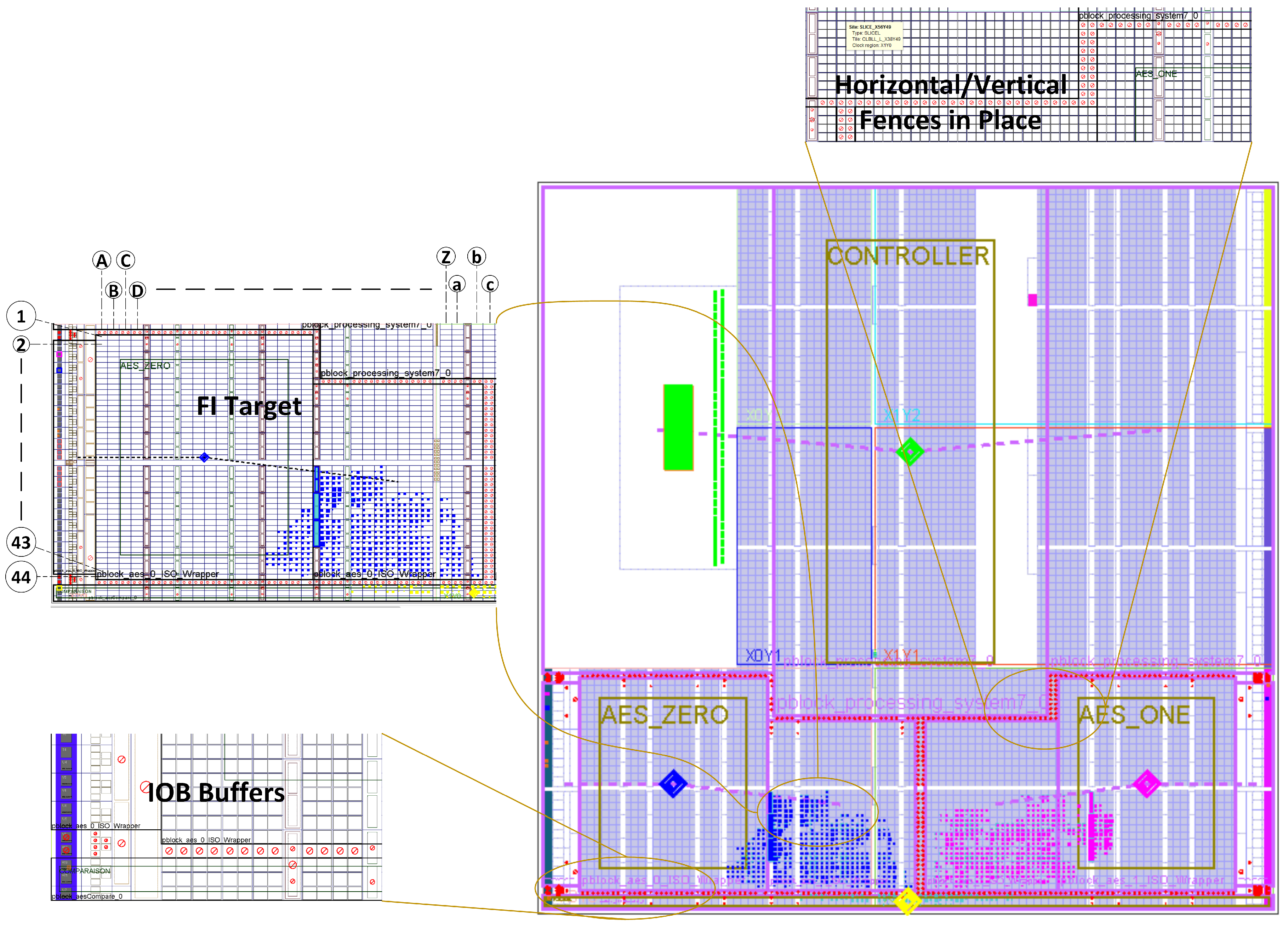
The layout of our IDF-based designs, as shown in
Figure 5, depicts the placement of isolated modules, FI target for our evaluation methodology and IDF-based fences around the various resource such as FIFO, BRAM and IOB Buffers.To investigate and comprehend the effectiveness of IDF, two designs were compared; one with all the IDF and placement constraints and another without IDF constraints (with the same placement constraints as the first design). The FI algorithm mentioned in the previous section was run repeatedly, in several iterations for both designs, injecting non-intrusive SEUs and the effects of these SEUs were recorded. The results were obtained by performing FI in several PL locations which are marked in
Figure 5 for the reader’s visualization, along with the areas where the HW evaluation candidate AES_ Zero and AES_ One were located on ZynQ SoC Chip. Some of the results collected during this analysis are also tabulated in
Table 2 where the areas that correspond to the interconnections of the two AES modules are highlighted in boldface. It can be seen that those areas such as 43B and 25F showed a higher concentration of errors in the Non-IDF design because this is where the logic boundaries (AES _ Zero and Comparator module horizontally and AES _One vertically) were present. Critical routing bits of these modules were located without any isolation between them and our introduced SEUs resulted in a disconnection between logic. However, once the IDF was enabled and fences were placed around this area, the number of errors reduced significantly in those areas, as IDF ensured the placement of critical routing information with-in the specified isolated, p-block regions. Areas 1A-22L were mostly vacant slices, with minimum or no logic present, hence FI on these locations did not produce many noticeable errors.
From
Table 2, it is evident that once the IDF was incorporated in our design (and trusted routing was enabled by Vivado), the error rate reduced drastically for the areas that correspond to the interconnections of the two modules. However, the elimination of these errors that could lead to SPOFs is not cost-free. The trusted routing and design fence that were incorporated in the design reserved resources with-in the ZynQ SoC chip and these resources were thus essentially unavailable to our design.
Table 3 summarizes the total Zynq SoC resources available to our design in IDF and Non-IDF design environment along with the total percentage use of resources reserved by IDF by employing fences, trusted routing and modular isolations. By carefully analyzing the resources use obtained in
Table 3, we observed the following: (1) When IDF is enabled for a design, Vivado’s synthesizer reserves some resources from the chip and prohibits its usage in user design thus, creating a physical boundary; a separation between each isolated module which restricts the propagation of error in an event of system failure. (2) The size of resources that are effectively marked unusable, as a result of enabling IDF in a design varies and depends on (a) Number of isolated modules (b) Height of fence applied (c) Width of fence applied (d) Complexity of logic being implemented in terms of slice and primitive use (e) Number of global clocking components (f) Route/signals exempt from isolation. The resource overhead that IDF incurs thus, may vary from design to design. However, the resource overhead in comparison to its effectiveness against fault containment over-weighs itself.
Using Vivado design power estimator we collected the power consumption data for our IDF and Non-IDF design which is presented in
Table 4. It can be seen that the power consumption is almost the same in both cases and the use of IDF seems to have little impact.
The timing summary of our implemented modules is presented in
Table 5. In this case, there is an increase of the maximum frequency of operation when using the IDF but the difference is not large.
Finally, let us discuss the benefits in terms of fault injection acceleration provided by the proposed methodology. As discussed before this acceleration is the main objective of the proposed methodology. There are two main components in the time needed for fault injection that depends on the methodology. The first one is the generation of the bit-streams used for the fault injection and the second is the time needed to download those bit-streams to the FPGA to test the error.
For the first component, our novel, one frame PFT is generated in real time in comparison to the partial bit-streams generated by Xilinx tools. It is to be noted here that the average time to generate a partial bit-stream taken by Xilinx Vivado Design Suite 2018.2 on our average PC with Intel(R) Core (TM) i5-4500M Quad core CPU @ 2.50 GHz and 8.0 GB RAM was roughly 10 minutes whereas our PFT was generated in 0.2 s thus achieving a 3000× reduction in the time needed. It must be noted that the proposed methodology also eliminates the need to store the partial bit-streams used for fault injection.
Table 6 gives the sizes and generation times of the different options for the for the XC7020 bit-stream.
For the second component, the time needed to download the bit-stream to the device, the size of the Zynq XC7Z020 All Programmable SoC full bit-stream is 4,045,564 bytes and its configuration time using PCAP in a standalone, bare-metal environment is measured to be 32 ms in [
30]. As the size of the partial bit-stream is smaller than the full bit-stream, it requires less configuration time, approximately 1 ms. However, Xilinx tools cannot generate a partial bit-stream which targets and configures only one frame [
5]. This is where the proposed PFT provides a significant advantage by enabling the single frame modification that can be done in less than 0.015 ms. The times are summarized in
Table 7 and corresponds to an average time, measured between the beginning and end of DevC DMA transfer function call with PCAP clocked at 100 MHz whereas, for our proposed PFT, PCAP was clocked at 50 MHz. It can be seen that the proposed methodology reduces the time needed to download the bit-stream that injects the failure by a factor of approximately 67× compared to the previous scheme that performs fault injection by downloading larger partial bit-streams over the PCAP interface [
5,
6,
7,
13].
As a summary, the results discussed show that the proposed methodology is able to provide very significant reductions in both the time needed to generate the partial bit-streams needed for fault injection and also in downloading those to the configuration memory of the FPGA.

 ,
, 


