Article

Development of an Optical Signal-Based IPS from an MCU-SoC

by
Borja Rubiano-Muriel
*,
José Luis Lázaro-Galilea
,
Alfredo Gardel-Vicente
,
Álvaro De-La-Llana-Calvo
and
Ignacio Bravo-Muñoz
Department of Electronics, University of Alcalá, Alcalá de Henares, 28801 Madrid, Spain
*
Author to whom correspondence should be addressed.
Electronics 2020, 9(5), 782; https://doi.org/10.3390/electronics9050782
Submission received: 30 March 2020 / Revised: 28 April 2020 / Accepted: 2 May 2020 / Published: 9 May 2020
(This article belongs to the Special Issue New Applications and Architectures Based on FPGA/SoC)

Abstract

:
In this work, we have studied the integration of an optical signal-based Indoor Positioning System (IPS) capable of supporting multi-access discrimination techniques. The research analyzes the different techniques and conditions that can be used to develop an IPS using a microcontroller unit (MCU)-based system-on-chip (SoC) systems. The main goal is to be able to integrate into the MCU both the hardware and software requirements for an IPS detector. In this way, different strategies that can implement multi-access discrimination using Frequency-division multiple access (FDMA) have been tested, such as I/Q demodulation, digital filtering, and discrete Fourier transform (DFT). This analysis has found a good technique to be executed in an MCU-based SoC, the DFT implemented through the Goertzel’s algorithm. The empirical tests carried out concluded that, using only one an MCU with the required HW and tuned SW, 15 position measurements per second were computed, with high accuracy in the 3-D positioning, with errors of less than 1 cm in a test area of 3.5 × 3.5 m 2 . The main contribution of the paper is the implementation of the optical signal based IPS in an MCU-SoC that includes signal acquisition and processing. The digital filtering or spectral processing for up to 16 received signals makes this IPS system very attractive from a design and cost point of view.

1. Introduction

Nowadays, in almost every facet of our lives, we are supported by positioning systems either outdoor (through global satellite systems and related applications) or indoor, where we can enjoy multiple benefits from the development of Location Based Services (LBS). The great popularity of mobile devices around the world is one of the causes for the growing development of LBS [1,2]. In the last years, significant research efforts have been devoted to develop indoor positioning systems and applications. Knowing indoor position is of great interest in different research fields—in logistics applications to perform different tasks in intelligent factories [3] it is also used to move objects [4], to help people [5] and to locate users in professional or leisure activities [6,7]. The global market is aware of these applications and therefore LBS and its supporting technologies attract a lot of interest [8,9]. Indoor positioning systems (IPS) are also well integrated into day-to-day activities [10,11,12,13], providing additional application capabilities with significant added value. Different indoor location systems have appeared in last years: based on artificial vision [14], ultrasounds [15], optical signals [16], radio frequency identification [17], wireless local area network [18]. IPS based on optical signals and ultrasound, are low cost solutions, easy to deploy with high accuracy location results in a wide range of applications (components to develop them are low cost with minimal maintenance). Currently, there are many requirements to consider when choosing the right technology for an IPS application. As has been discussed in Reference [19], some decision parameters are—accuracy, precision, coverage area, required infrastructure, market maturity, privacy, update rate, user interface, system integrity, robustness, availability, scalability, number of potential users, degree of intrusion, and legal coverage, and so forth.
However, indoor position estimation still lacks a low-cost and possible to generalise solution that would allow LBS to adapt to different indoor scenarios. The ease of implementing a simple positioning system, the possibility of having an accurate system, inexpensive and applicable to many indoor environments at the same time, and the rapid adoption by the industry are some of the great challenges today. Advances in technologies facilitate the improvement in the performance of sensorial systems. The choice of sensors will depend on the user’s requirements. In the case of IPS based on optical signals, the traditional solutions had an accuracy in the range of ten centimeters. Currently different IPS systems [16,20,21] have been developed using Angle of Arrival (AoA) techniques based on Position Sensitive Devices (PSD), providing high precision (in the range of millimeters). Recently there have been many publications related to IPS based on the use of visible light positioning (VLP) emitted by building lighting systems; in our case, within the GEINTRA research group of the University of Alcalá, work has been carried out for a long time on positioning systems and one of the lines addressed from the beginning was the use of optical signals (originally Infrared, -IR-). More recently, the techniques developed have been adapted to work with VLP, obtaining a high performance system, nothing invasive and with few infrastructure requirements [16,20,21,22,23,24,25]. In relation to optical signal-based IPS, several research works use LED lighting; the authors of References [26,27] obtained relevant positioning data to evaluate accuracy and precision. In Reference [26], each LED (from the lighting system) sends spatial 3D coordinates and an image sensor receives the signal. By means of numerical analysis, the authors showed the position of the receiver can be measured with an accuracy error of less than 1.5 m. If we compare the use of image sensors with the use of PSD sensors (and if only positioning functions are to be carried out) we use an image sensor, we will also need a computer, or similar system, to process the images and run the positioning algorithms. That, besides being much more expensive, gives less measurements per second of the position of the agents, worsening, the more agents there are in the scene. In previous works like Reference [16] we have been able to compare that the PSD and Field Programmable Gate Array (FPGA) based system obtained position measurement rates 2 orders of magnitude higher than the image sensor based system. In Reference [27], the receiver obtains the coordinates of the LED light from a received identifier. The results show a maximum horizontal error of 10 cm in a test area of 5.4 m by 7.5 m, and a height of 3 m.
In Reference [28], they proposed the use of four LEDs that transmit the 3-D coordinates achieving positioning errors below 10 cm. In Reference [29], they address the development of IPS based on the received signal strength (RSS) of the received visible light, using multiple photodiodes in the receivers. The results obtained show an average positioning error of 20 cm over an effective positioning range of 1.8 m. It should be noted that these systems have the disadvantage of attenuating the RSS with greater distances and angles. In Reference [30] a system that determines the position by triangulation is presented; it emits IR signals from the mobile agents and determines the angle of arrival with a set of photodiodes (detectors) located in the environment. The test area was 7 × 2 m 2 , obtaining errors of up to 70 cm. The disadvantage of this system is the difficulty of initial deployment and calibration. Regardless of the technology used, the most common problems faced by IPS are related to signal quality, deployment strategy of positioning anchors (antennas, receivers, transmitters, etc.), non-line-of-sight situations, dynamic location, interference from other devices, and similar to outdoor positioning, multipath effects [31]. Regarding the approach of the present paper, little is detailed in the publications reviewed so far; it is about the hardware resources to carry out the circuits and the algorithms of the positioning application. In our case, which is positioned by angle of arrival of the signal coming from different LED lamps, and which is based on FDMA as a technique for multiple-access discrimination (MAD), so far they have been implemented in a Field Programmable Gate Array (FPGA) based card. This card works together with another acquisition card developed by the research group from a PSD sensor. Given the cost of the FPGA-based system, the complexity of the development of the final prototype cards, and the time required in debugging any change, it has been proposed to implement the system of signals filtering and calculating the position of different emitters—LED—simultaneously, in an MCU which also incorporates the ADC converters. In this paper, we do not seek to propose input on new access control mechanisms but to use already proposed mechanisms such as those contained in Reference [32]. There they gave an overview of the current state-of-the-art studies on VLP systems classified according to the multiple access technology used. The main contribution of the paper is the analysis of different mechanisms that can be used within an MCU/SOC to be able to make acquisition, conditioning, and processing of the signal. The design goal is how to do everything on one chip to get a fully integrated IPS within an MCU; that is to say: a low-cost embedded system, with real-time execution. Also, debugging times are reduced during the development phase compared with FPGA-based designs, making the final platform cheaper. Note that we have also developed the system using an FPGA-based card, a MicroZed 7020-Zynq SoC-development board, which increases the system cost by about $300. This higher cost is unfeasible from a massive deployment point of view. The customization of the design using a system based on a Zynq SOC chip, jointly with the acquisition systems for the PSD sensor currents, is complex, error-prone, with different versions of the PCB prototypes, which will be very costly both in time and money.
However, if everything needed by the system could be implemented using a MCU based card or customizing the design using a MCU chip, the solution will be low-cost, with much lower development time to obtain the entire electronic design and PCB development. Moreover, in software debugging phases, much less time will be required.
This document is structured, in addition to this brief introduction, in a Section 2 that describes the Background of the existing systems and those developed by the developed by the GEINTRA Group; then, in Section 3, a theoretical review is made of the possible methods to carry out the Digital Implementation of FDMA on MCU for the development of an IPS. Finally, in Section 4, a wide analysis about viable and not viable solutions, as well as obtained results and the precisions that can be reached with IPS developed on SoC based on MCU are presented.

2. Background

In this section we introduce the positioning system we have developed, the sensor used in it and the techniques to get to deduce the position of the agents. In addition, the multiple-access discrimination techniques are related, in case the signals coming from several emitters are received in the detector; techniques we have been tested in research works in our group (it is out of the scope of this work) and are going to be analysed to be implemented inside the MCU in this research. As it has been indicated, this work is framed within the development of IPS based on the use of visible light emitted by the lighting systems of the buildings (VLP), which is one of the IPS developed within the GEINTRA research group of the University of Alcalá, which has been working in this area for a long time. More specifically, this work is related to the previous works discussed in References [16,20,21,22,23,24,25] which have resulted in a high-performance system.

2.1. IPS Based on PSD

Our proposal for IPS uses the environment’s own lighting (based on LED emitters) as an emitter, allowing for a reduction in costs and complexity of the infrastructure. For the development of the receiver our system is based on a PSD sensor, which generates currents related to the impact point of the received signal on the sensor surface; these currents will be converted into proportional voltages in the system’s signal acquisition and conditioning block. The technique used for the determination of the position is the AoA determination, as it can be seen in the scheme represented in Figure 1.
The PSD sensor consists of 4 anodes and a common cathode (Figure 2); from these anodes a signal amplitude will be obtained representing the impact point of the light beam on the PSD surface. This impact point can be calculated using the Equations (1) and (2) obtained from Reference [20]. Equations (3) and (4) show the expressions that relate the line angle connecting the emitter in space to the point of reception of its signal on the PSD, where (x,y) is the point of impact of the optical signal on the surface of the PSD, f the focal length of the coupled optical system, and ( θ y , θ y ) the components of that angle. If only one signal was received from a emitter and the angles of rotation of the agent were not known, the possible points (X,Y) in the plane of motion would belong to a circle centered on the orthogonal projection of the emitter position to the plane of motion. However, if, for example, the angles of the signals from 3 emitters were available, the position and angles of rotation of the agent could be calculated, but that is outside the scope of this work and the authors already have a proposal and results for this in Reference [25].
x = L X 2 ( V o 2 + V o 3 ) ( V o 1 + V o 4 ) V o 1 + V o 2 + V o 3 + V o 4 ,
y = L X 2 ( V o 1 + V o 2 ) ( V o 3 + V o 4 ) V o 1 + V o 2 + V o 3 + V o 4 ,
θ x = arctan x f
θ y = arctan y f
where V o j are the voltages obtained after passing the current of the 4 anodes of the PSD through transimpedance amplifiers [20]. Although the focus of the work is not on the sensor but on the electronics, in order to help the reader understand it, it should be remembered that a lens must be attached to the PSD. In the cases of the current developments of our research group we are working with 8 and 16 mm lenses, although we have worked and developed studies with other focal values. In previous works [20,21], procedures and mathematics were developed to be able to calibrate aspects such as: electrical parameters of the sensor and of electronic components, precise focal of the lens, optical centre of the system, distortion parameters, rotation and translation matrixes of the sensor with respect to space, and so forth.

2.1.1. Multiple-Access Discrimination Techniques

In multi-access scenario the different emitter signal will impact simultaneously at different points on the sensor surface and the currents that will be obtained by the anodes of the PSD will correspond to a sum of currents. Therefore, if signals from multiple emitters are received on the receiver (multiple-access), techniques are required to discriminate, from the signal provided by the PSD on each of its channels, the signal corresponding to each of the different emitters. Previous works developed on the research group, different ways to perform this discrimination have been carried out [25], concluding that a good alternative, and easy to implement and process, is the Frequency Division Multiple Access (FDMA). This discrimination method can be implemented using different techniques such as: In-Phase Quadrature demodulation (IQ demodulation), bandpass filtering (BPF) and Discrete Fourier Transform (DFT). All these techniques have given good results in previous works, without highlighting any of them specially. However, they differ in the way they are implemented and in the resources required for each of them to develop the sensor system. Therefore, in this work that intends to use an MCU based Soc replacing a SoC module Zynq from Xilinx (with FPGA and microprocessor), we will focus on choosing the technique that can be better implemented.

IQ Demodulation

IQ demodulation allows to obtain the amplitude of a previously known frequency signal (which we are looking for) by introducing a sine of the same frequency into the demodulator whose scheme is shown in Figure 3, where m t [ t ] is the signal obtained from the PSD sensor, s ( t ) is the sinusoidal signal that is introduced with frequency equal to that of the signal being sought and A r will be the amplitude of the demodulated signal. This demodulator use a Low-Pass Filter (LPF). In our case it would be necessary to have an I/Q demodulator for each of the possible frequencies emitted from the emitters, and for each of the 4 channels of the PSD.

Band-Pass Filters

Discrimination using bandpass filters consists of applying to output signal of each PSD channel a number of filters equal to the number of emitters (each centred on one of the frequencies to be detected) and calculating the RMS (Root Mean Squared) value of the signals obtained. This implies, in the case being carried out in this IPS, a total of 16 filters (4 channels × 4 emitters). In the Figure 4 it is shown a scheme of the filter battery to be implemented for each one of the PSD channels, where m t [ t ] is the signal obtained from the channel, f i is the central frequency of the filter, and if the signal coming from each emitter received by that channel.

Discrete Fourier Transform

The DFT allows to obtain, from a received signal, the different sinusoidal tones of the different frequencies that compose it (Figure 5 and Figure 6). Therefore, by performing the DFT of our signal, we will obtain peaks of different values (depending on the RSS and the position in PSD surface it is received) in frequencies that correspond to the tones emitted from the emitters (frequencies at which it is emitted). From the values of the peaks, and applying Equations (1) and (2), the point of impact in the PSD surface of the signal from each emitter will be calculated, and subsequently, by means of Equations (3) and (4), the angles used to determine the position of the emitter in relation to the receiver.

2.2. FDMA Implementation on FPGA Devices

In the first proposal for IPS implementation, these discrimination techniques were implemented using an SoC Zynq of Xilinx (Figure 7). Working in parallel in the FPGA and processing in software (executed in the silicon ARM processor that includes) the calculation of RMS values are obtained with great results for both techniques, based on IQ demodulation and based on the use of bandpass filters (especially the latter). One demodulated signal per channel and emitter can be obtained using the FPGA Digital Signal Processing modules, leaving the rest of the resources free for further processing.
The bandpass filters used in the tests carried out were of the FIR type. The FPGA provides the possibility of performing these parallel operations in a very short time, obtaining one output value for each input sample (along with the previously captured data window).
However, both the cost to develop the customized printed circuit boards (PCB) and SoC chips are much more expensive than an MCU solution. On the other hand, when designing and building PCBs, FPGA designs are more expensive, require more time and more electronic components. Besides, in the debugging phase, every small change involves a long simulation time or slow down in working with FPGA. Nevertheless, this is not the case when working with MCU chips. The compilation and debugging step by step the code, are fast and convenient tasks. For these reasons, in this paper, we propose to study of the digital implementation of the FDMA technique fully supported in an MCU, including data acquisition done by internal ADCs.

3. FDMA Implementation on MCU

When implementing systems and algorithms to carry out multiple access discrimination using FDMA, MCU-based systems have also a number of disadvantages and problems compared to SoC with FPGAs, The main disadvantage of the implementation in an MCU is the time needed to acquire signals and perform signal processing. In MCUs, the fact that they cannot process in parallel (except that some peripheral device can work at the same time as the processor) is a significant limitation. The time needed to process some techniques may lead to making the use of MCUs unfeasible. In the previous investigations carried out by the research group, it was concluded that the error obtained among the different alternatives to implement FDMA oriented to multiple access discrimination, was very similar in all of them. Therefore, a requirement analysis of these alternatives will be done taking into consideration the conditions to implement them in MCU devices to decide which of them are suitable to execute in the proposed platform.

3.1. IQ Demodulation

IQ demodulation is a good implementation alternative when working on FPGAs, since it allows obtaining results in real time; with each sample provided by the acquisition system, a positioning output result can be obtained, based on that sample and the previous ones. This is possible thanks to the parallel processing that can be done with these devices. Demodulators similar to the one shown in the Figure 3 are required, with a l p h a being the number of channels (4 in our application) and b e t a being the number of agents to discriminate. Each one of these demodulators implies the implementation of two low-pass filters, two multiplications and a module calculation: so, given the computation times required by these modules, a priori it will not be an option to consider.

3.2. Band-Pass Filters

Discrimination by digital Band-pass Filters is done using FIR or Infinite Impulse Response (IIR) implementations. FIRs generally give good results but need to be of a much higher order than IIRs, consuming more time or resources. The order of the filter will result in a delay in the output signal of n cycles being n the order of the filter. Therefore, in order to avoid a delay that makes its implementation unfeasible in an MCU, for this initial analysis, we will choose the option that needs less order (therefore, it will reduce the computation time). Moreover, after filtering the signal, it will be necessary to calculate the RMS value of each of the signals obtained by each of the PSD channels. Then, this procedure will have to be performed α × β times. An excellent option to implement the necessary filter IIR would be the structure of its DirectForm-II, shown in the Figure 8.
This structure can be programmed through a sequential process, which makes it easy and straightforward to be programmed and executed in an MCU. It also simplifies the construction of higher-order filters. These filters are usually built considering parameters with floating-point numbers. Nevertheless, due to the high computation time to perform floating-point operations in an MCU, we have studied the possibility to reduce the processing time of this type of filter, using fixed-point data, whenever possible, using numbers power of two. This optimization implies a loss of quality in the filter, as shown in the comparison of Figure 9 and Figure 10, in which the band pass filter is executed with floating-point and approximated 2 n integer numbers, respectively.
By approximating the filter coefficients to integer numbers approximated to a 2 n number, the frequency response is considerably widened so that the noise bandwidth becomes greater, reducing the SNR.
In addition, if this alternative is chosen, great care must be taken when selecting the frequencies of the emitters so that they do not fall within the bandwidth of nearby frequencies used by other emitters.
On the other hand, we observe that the filter area without attenuation is no longer flat. This could be a problem in some applications, but in our case, as the filters placed in all the channels have the same structure, for the same frequency, we will have the same multiplication factor.
As the post-processing consists of relations between the RMS values of the different filtered channels, this gain will affect all of them equally and is therefore compensated.
Section 4 will show the results of the time required to carry out this processing executed in an MCU and other considerations about this possible alternative.

3.3. DFT—Discrete Fourier Transform

For the calculation of the DFT, the first option considered here, it is to perform a DFT (FFT is possible as we have a power of two number of samples) of each of the α channels of the PSD and maintain the values obtained from the resulting signals for each of the frequencies at which the different emitters work. This method has the disadvantage that, in terms of processing time efficiency, we would be calculating values that are not useful for our application (those of all the frequencies different from those of the emitters used). Therefore, it is proposed to use the Goertzel algorithm [33] that allows calculating the value of a DFT for a given frequency, providing a substantial improvement in the computation time because the whole FFT should not be performed. However, this algorithm will have to be repeated as many times as the number of frequencies used for each one of the 4 channels of the PSD. The transfer function of the algorithm and its flowchart are shown in the Equation (5) and Figure 11:
H k ( z ) = 1 W N k z 1 1 2 c o s ( 2 π k / N ) z 1 + z 2 .
Since what we want to know is the DFT value for a given frequency N, it will only be necessary to know the value of y k [ N ] , which allows us to rewrite the algorithm eliminating the terms that do not imply feedback and to perform those operations only after having made the N necessary cycles to obtain the values, deleting unnecessary calculations during the transient. Thus, for the Δ N samples, the complete algorithm needs to perform Δ N multiplications, making the computation time linear to the number of samples N. This alternative together with the previous one, are the ones to analyze their implementation in an MCU, since it is considered that the computation time they require can make it feasible their execution in real-time (to obtain around 20 positioning measurements per second), with the advantages that all this would imply.

4. Results

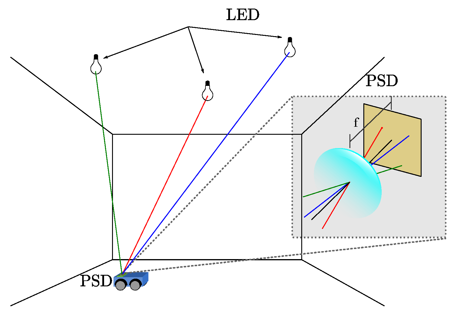
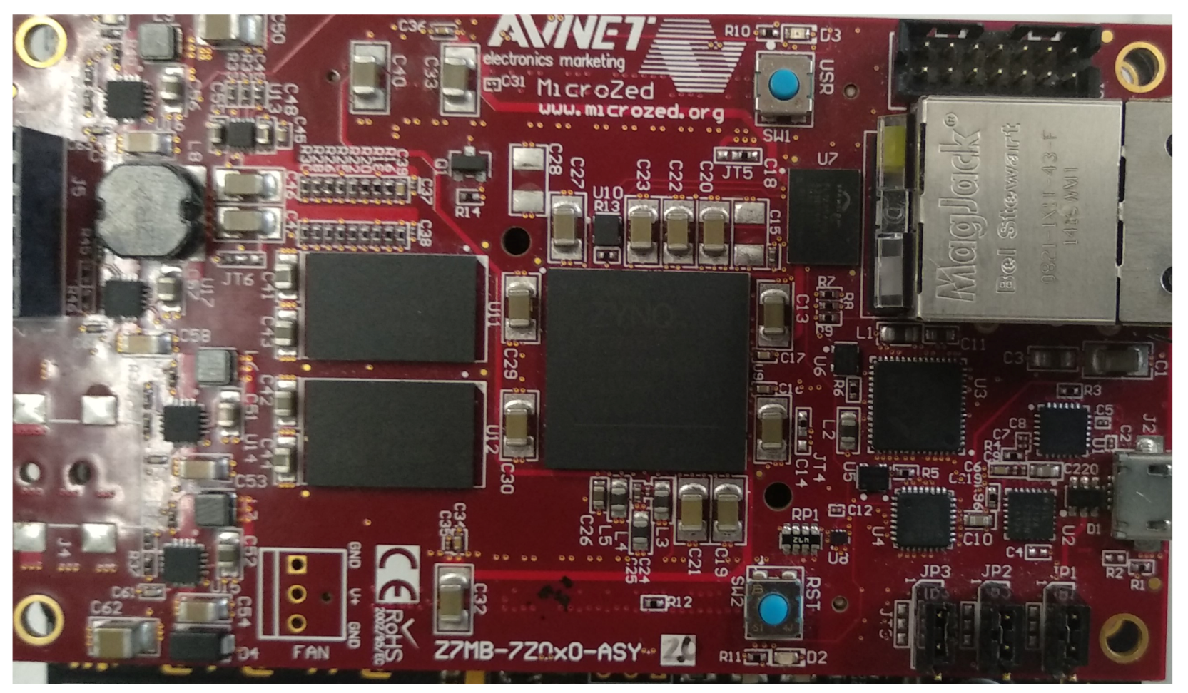
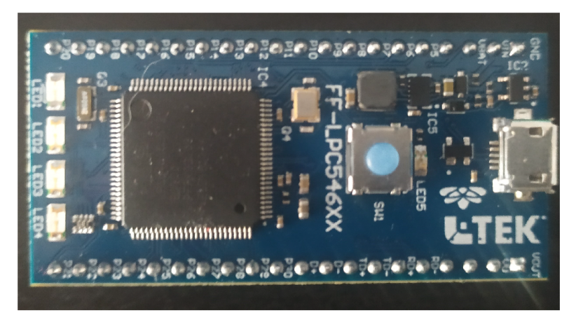
In this Results section, the feasibility of the last two proposals will be analyzed, with emphasis on the time needed to obtain the position of the emitters with respect to the detector (or vice versa). For this purpose, the L-Tek FF-LPC546xx circuit, based on an NXP Cortex M4 MCU operating at 180 MHz, will be used (
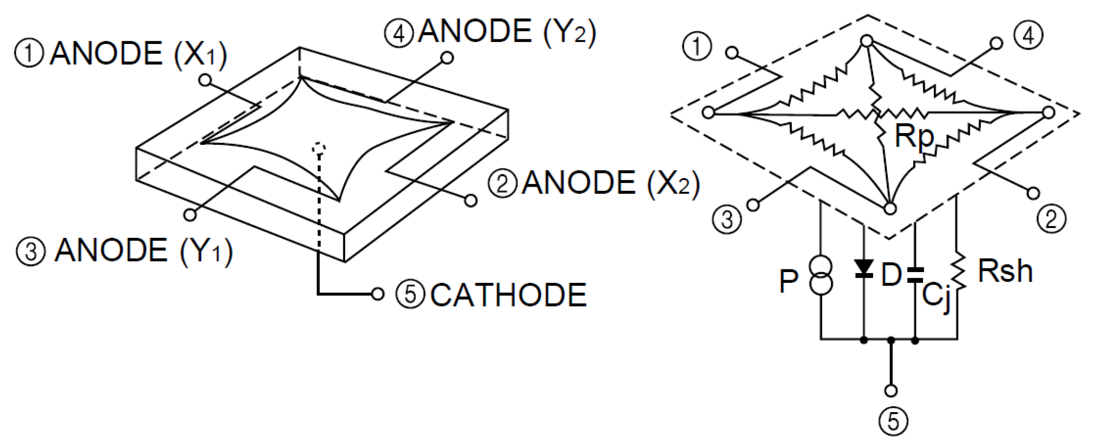
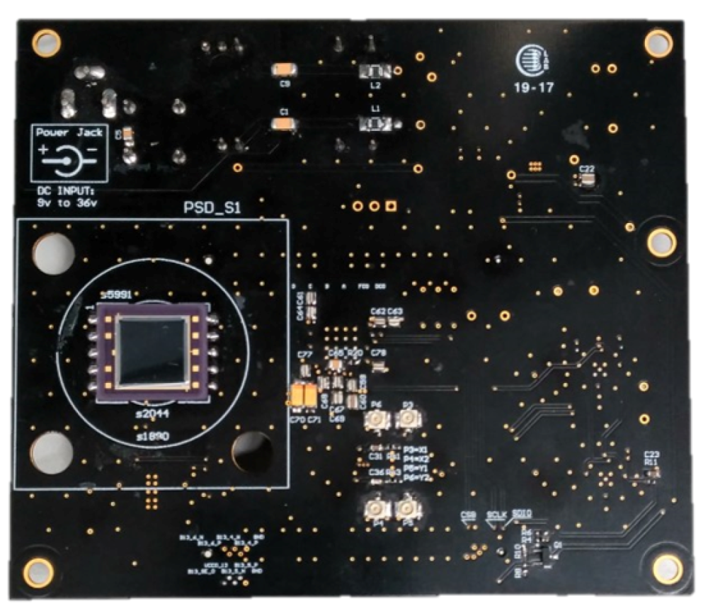
Figure 12). This device includes several ADC converters that are capable of responding to the conversion frequencies needed. Searching for an MCU with the required capabilities makes the solution to be a final application SoC for our application, reducing the necessary external hardware. For the tests, we are going to consider an IPS formed by the PSD S5991-01 from Hamamatsu Photonics (Hamamatsu, Japan) with 9 × 9 mm 2 area detector. 
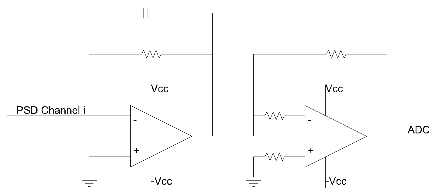
Figure 13 shows the different stages used to amplify the output signals of the PSD sensor. This modular design is done to avoid the influence of external light, as the external signal will be a continuous (or low frequency signal or noise. The first stage is configured so that the signal received at the sensor (emitted signal added to the external signal) does not saturate the output of the amplifier. In addition, a low-pass filter is implemented in this first stage to obtain a signal with the necessary bandwidth at the output. After this stage, the low-frequency components such as the signal from the sun (continuous) and the light from other sources such as fluorescent bulbs (100 Hz) are filtered. Finally, the last amplification is performed to adjust the signal to the ADC span. This avoids the possible saturation of the ADC input depending on the outside light. The 
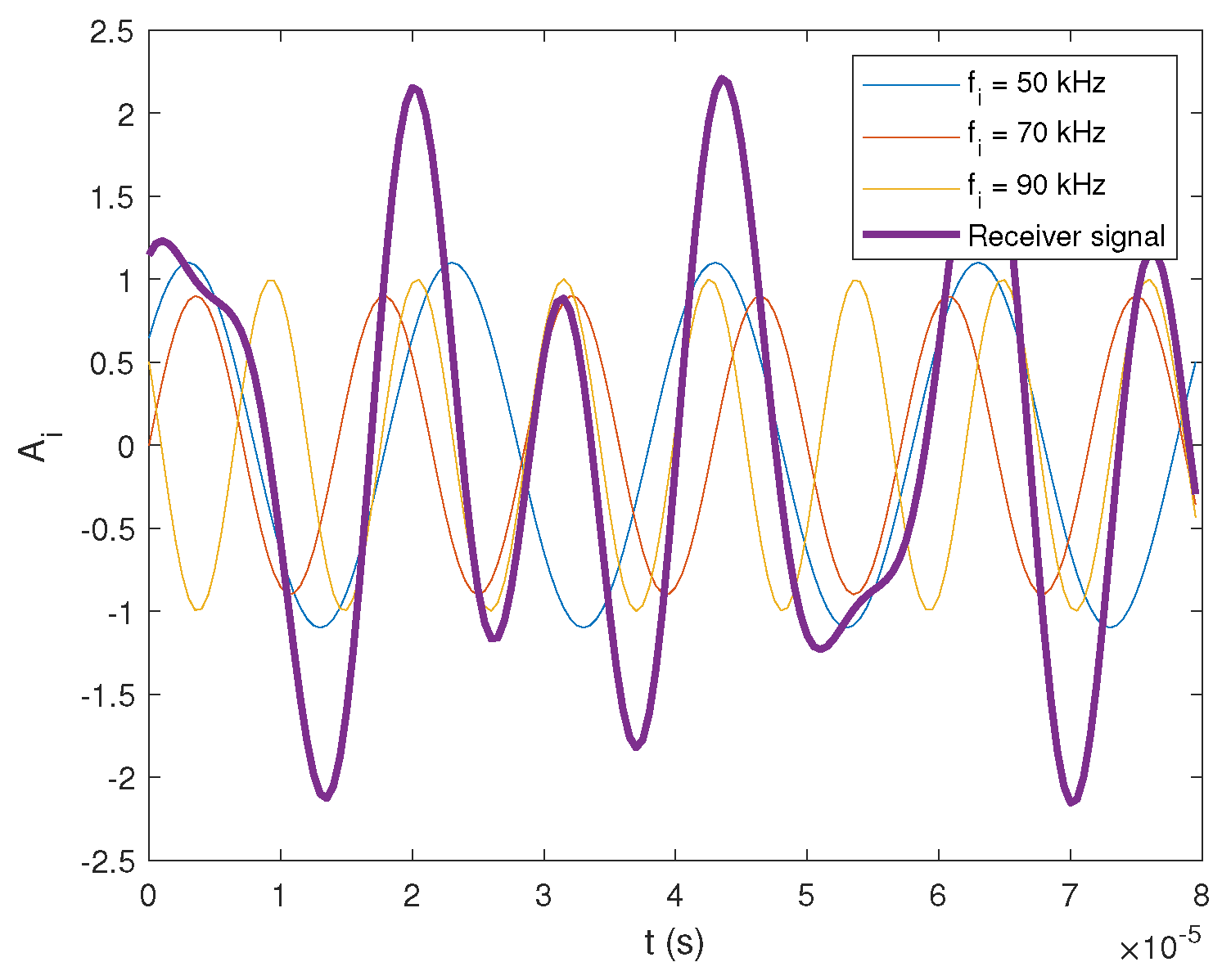
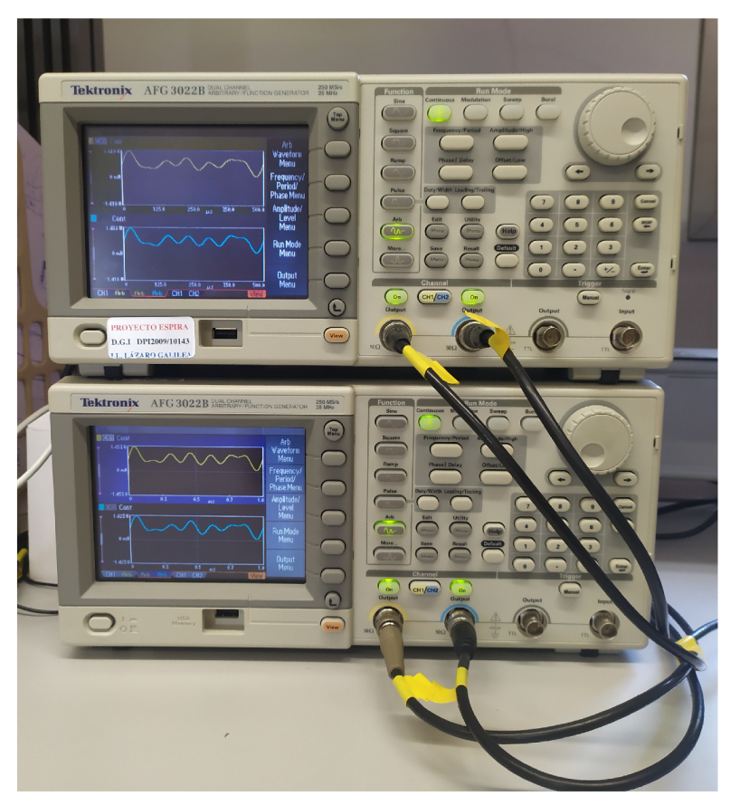
Figure 14 shows the conditioning card used in conjunction with the PSD sensor. Four modulated LED emitters with 6 kHz, 8 kHz, 10 kHz, and 14 kHz sinusoidal signals will be used. Since high modulation frequencies are used, the feeling for the user is one of continuous emission. First, the computation time of both proposals will be analyzed, and then, for the most efficient one, the positioning results will be evaluated using the indicated MCU.

4.1. Results Using Band Pass Filters

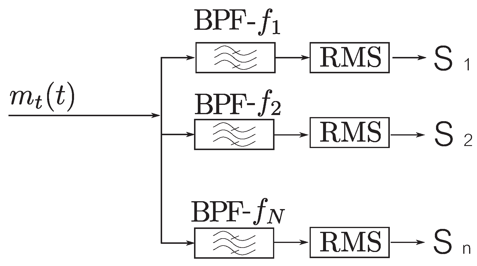
For the implementation of FDMA using bandpass filters with an IIR structure, it is necessary to execute the IIR filter code 16 times, and perform 16 calculations of RMS values.
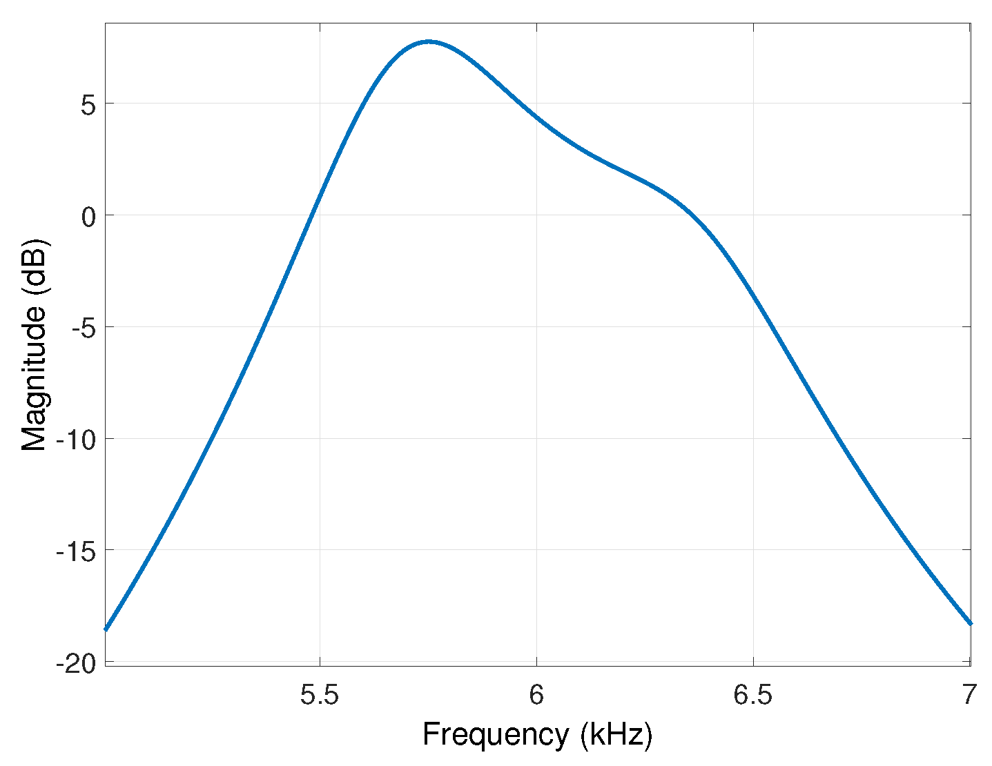
IIR filters with the direct form II structure will be used, of order 2 with 3 sections in series. This means a final filter of order 6 and therefore a delay of 6/fs.
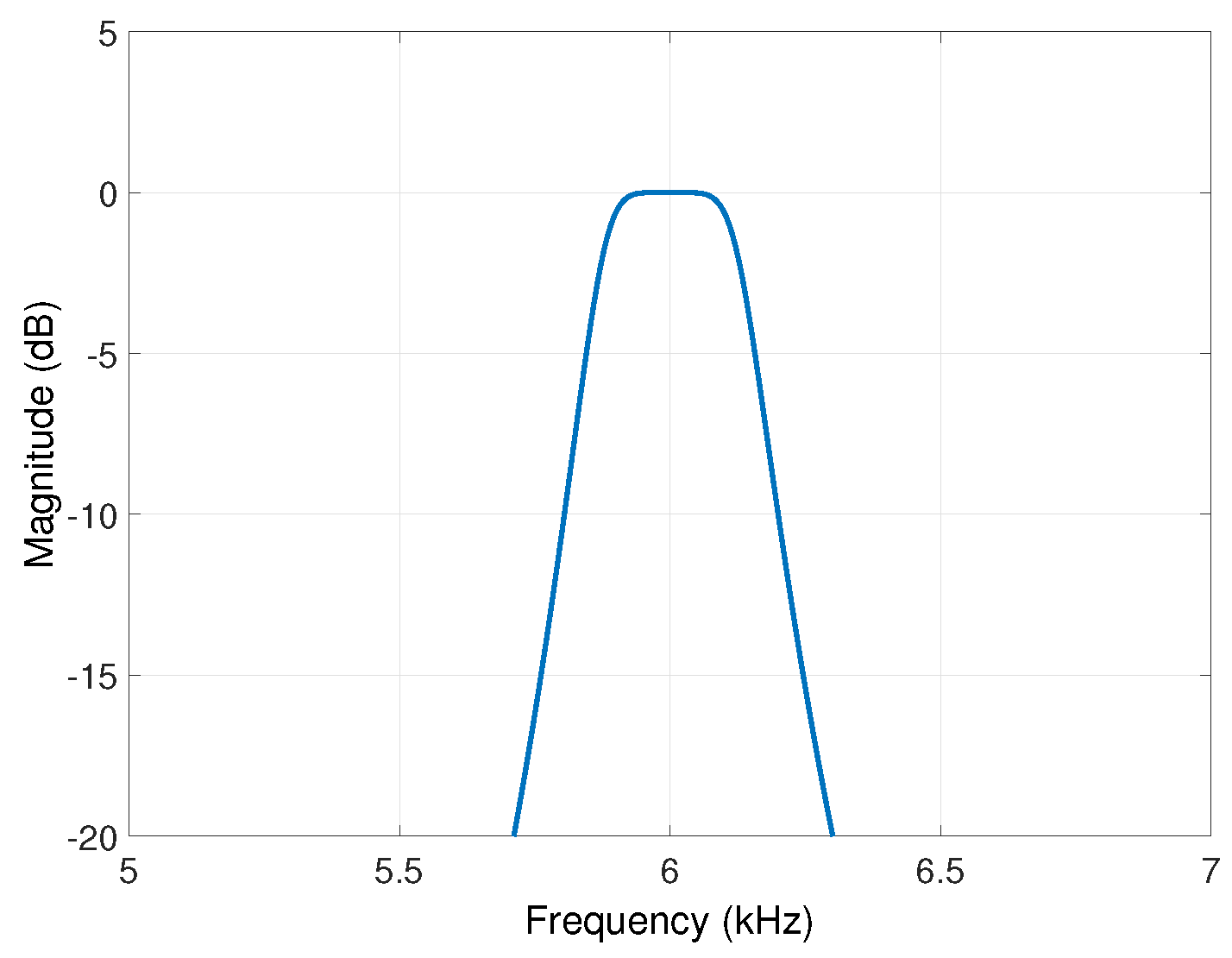
The different bandpass filters are modelled with the parameters shown in the Table 1. From now on, when we refer to one bandpass filter, we will be chosen as an example, the filter with a 6 kHz centre frequency, as the rest of the filters have similar comments.
Using the MATLAB Filter Designer tool, we obtain the filter coefficients that, as explained in the second section, will be converted to integers by multiplying by a power factor of two so that the coefficients that are originally 1 or −1 do not represent a computational burden. These operations will be carried out using bit-shift operations, whose processing involves a single CPU clock cycle. In the examples shown below, the filter is designed for a sampling frequency of 100 kHz and centered in 6 kHz. However, it is important to emphasize that the change of these parameters does not suppose a change in the computation time (as long as it remains of the same order). Therefore the time calculated for this filter can be taken into account for other values of sampling frequencies or filtering frequencies.
To check the processing time required to carry out the filtering for a frequency, it has been programmed twice, with two different versions: one working with floating point and the other with integers. The processing times are shown in the Table 2.
As can be seen, the time improvement when using integers power of two is very significant; it reduces time by almost 7 times. It should be noted, as indicated, that this result corresponds to a single filtering. In our case, 16 filters (4 frequencies × 4 channels) must be performed, also 16 RMS must be calculated. To calculate the total time needed, all these times must be added together. The process followed in the filtering is the next one: a window of previous samples is saved and each new sample that arrives is added to the previous ones eliminating the oldest one. In this situation, the filtering is carried out. Thus, a necessary time of 34.4 μ 
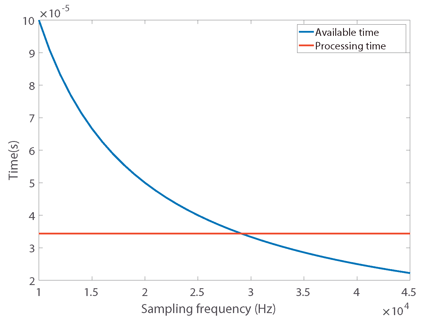
s is obtained for the 16 filtered, without taking into account the RMS calculation, or assuming that it can be done in parallel while the input signals are being sampled. Taking into account all the above, we proceed to calculate the maximum sample frequency that could be supported in the operating scheme (the system cannot support the arrival of new samples—one per channel—until it has processed the immediately previous ones). Figure 15 shows a comparison of the time needed for the filtering process (available time) and the time it would take for an acquisition system to deliver the next samples as a function of the sampling frequency. Note that the sampling frequency is limited to about 29 kHz without taking into account the RMS calculations. In this situation, for the emitter signal (14 kHz), approximately 2 samples per cycle would be available, which is clearly insufficient to be able to calculate an RMS value with guarantees in a not too high time. Consequently, this implementation proposal was discarded.

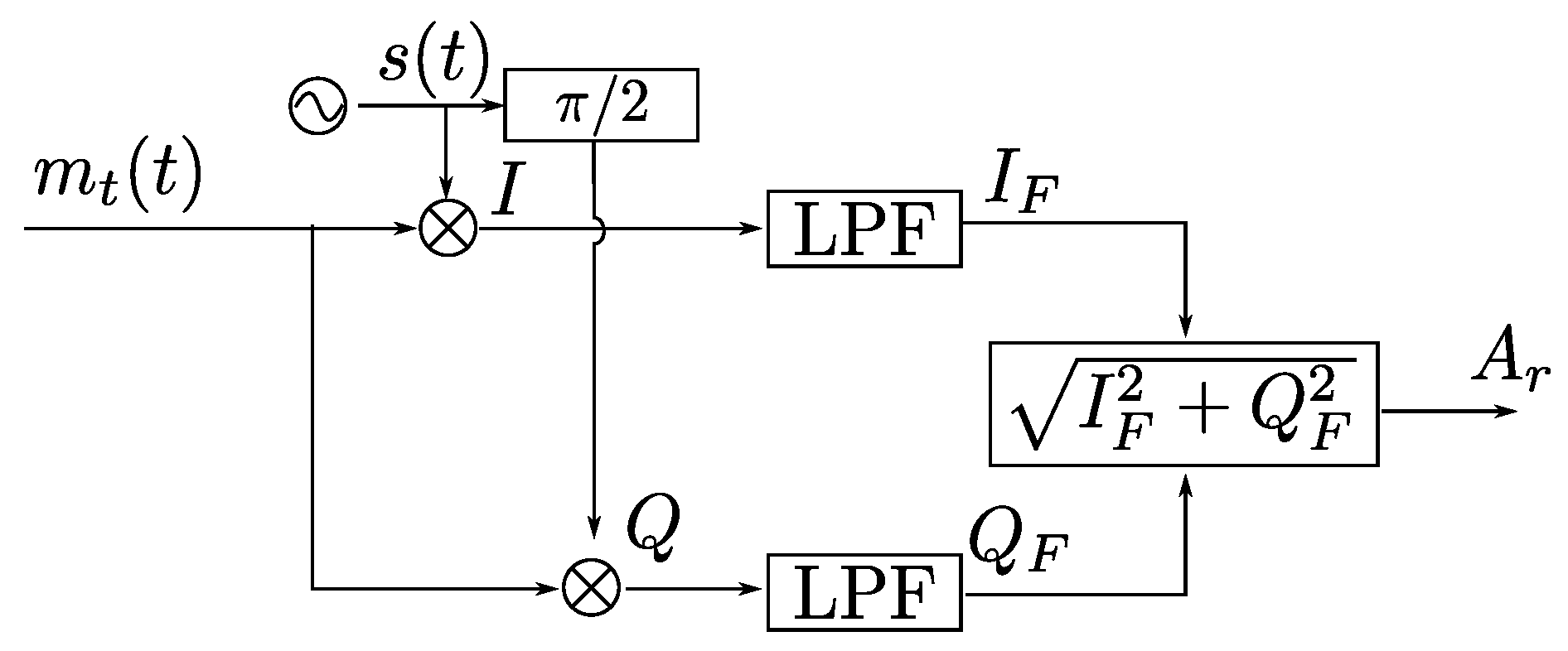
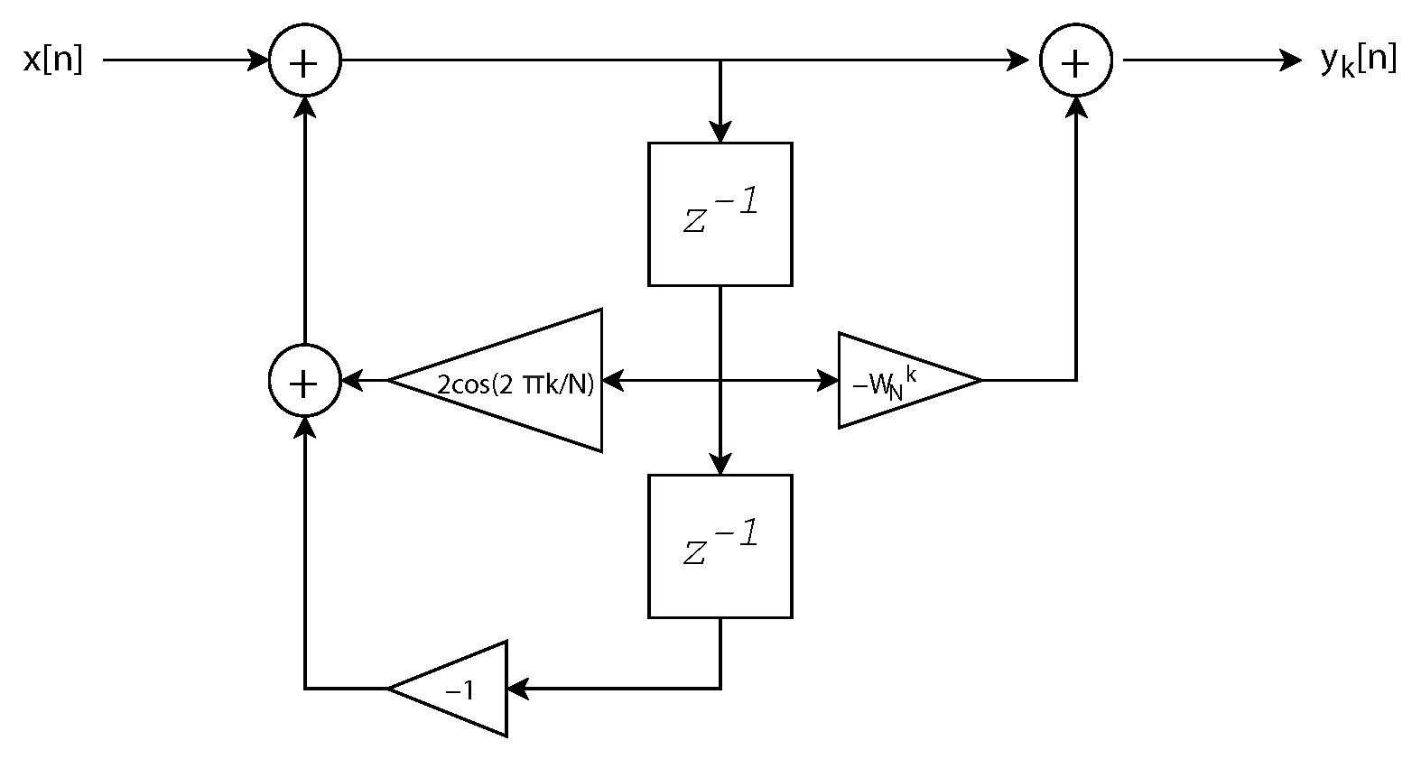
4.2. Results Using DFT

For the FDMA implementation using the Goertzel algorithm it will be necessary to run the algorithm 16 times. In this case, the algorithm will not be executed each time a sample of the signal is obtained. Instead, N consecutive samples of the signals of each PSD channel are saved and then the DFT is performed. If the operating scheme to be used is: acquire and store samples with the MCU’s internal ADC peripherals and, in parallel, process the DFT of the previous samples, the 16 executions of the algorithm must be done in a shorter time than that of the capture of the samples. In order to determine possible sampling frequencies, desirable number N of samples and total processing times, we first calculated the time required by the Goertzel algorithm to process the DFT with different number of samples. After implementing the algorithm in the MCU, the times shown in the Table 3 have been obtained.
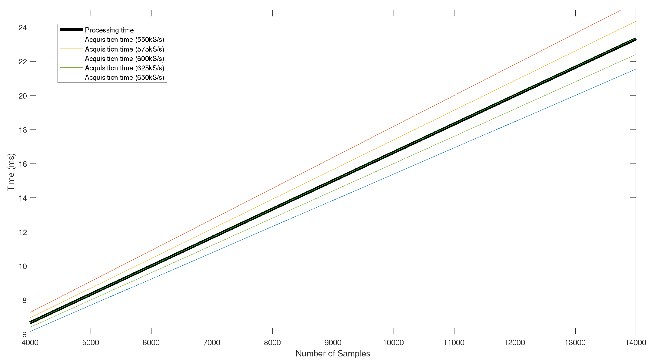
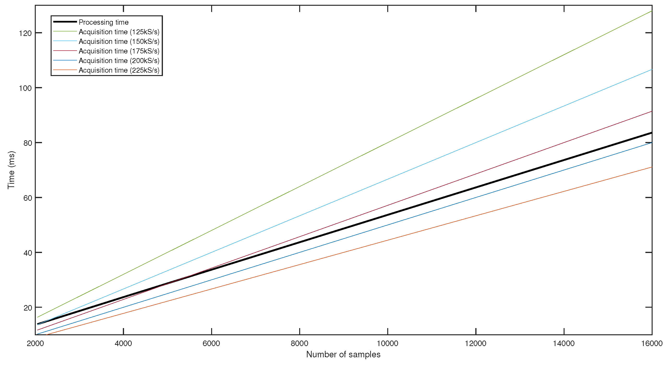
Taking into account these times and given that the algorithm needs to be processed 16 times every N samples, a graph has been made, as shown in Figure 16, in which the time needed to acquire a certain number of samples is represented as a function of the sampling frequency used (time available to process these samples in parallel with the acquisition), and the time needed to run the algorithm 16 times with that number of samples (time needed) we see the time available as a function of the sampling frequency and the number of samples chosen. This graph shows the sample frequency and number of samples that will be useful in parallel processing, where the CPU processes the data while the peripherals acquire the signals. In any case, the acquisition time has to be less than the processing time for correct execution.
Figure 16 reflects that there is more than enough time to process the samples while capturing the next ones. When determining the number of samples to be used and the sampling frequency, it should be kept in mind that if few samples are used, the result of the algorithm when calculating the DFT will be worse; in addition, less time will be available for the calculation of RMS values, the determination of the positioning point and the communication of results. On the other hand, if the number of samples is increased, the number of times per sample that the position can be calculated is reduced. A compromise solution will have to be reached that provides good results and an acceptable computation time (if, for example, it were decided to sample at 250 kHz each channel, using 8192 samples for each DFT calculation, more than 25.0 μ s would be available to process the results and report them). With the system already implemented, tests are performed considering synthetic data. For this purpose, two Tektronix AFG 3022B signal generators are used, introducing the signals that correspond to the signals that would be obtained with the positions of the emitters detailed in the Table 4. The signal generators and the signals used can be seen in the Figure 17.
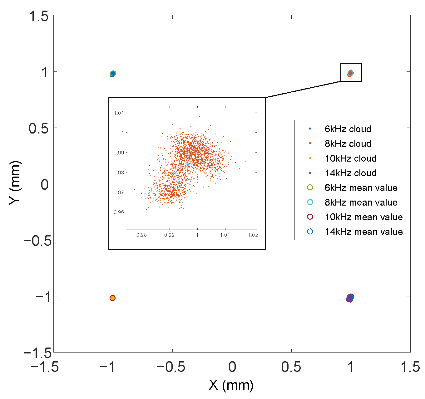
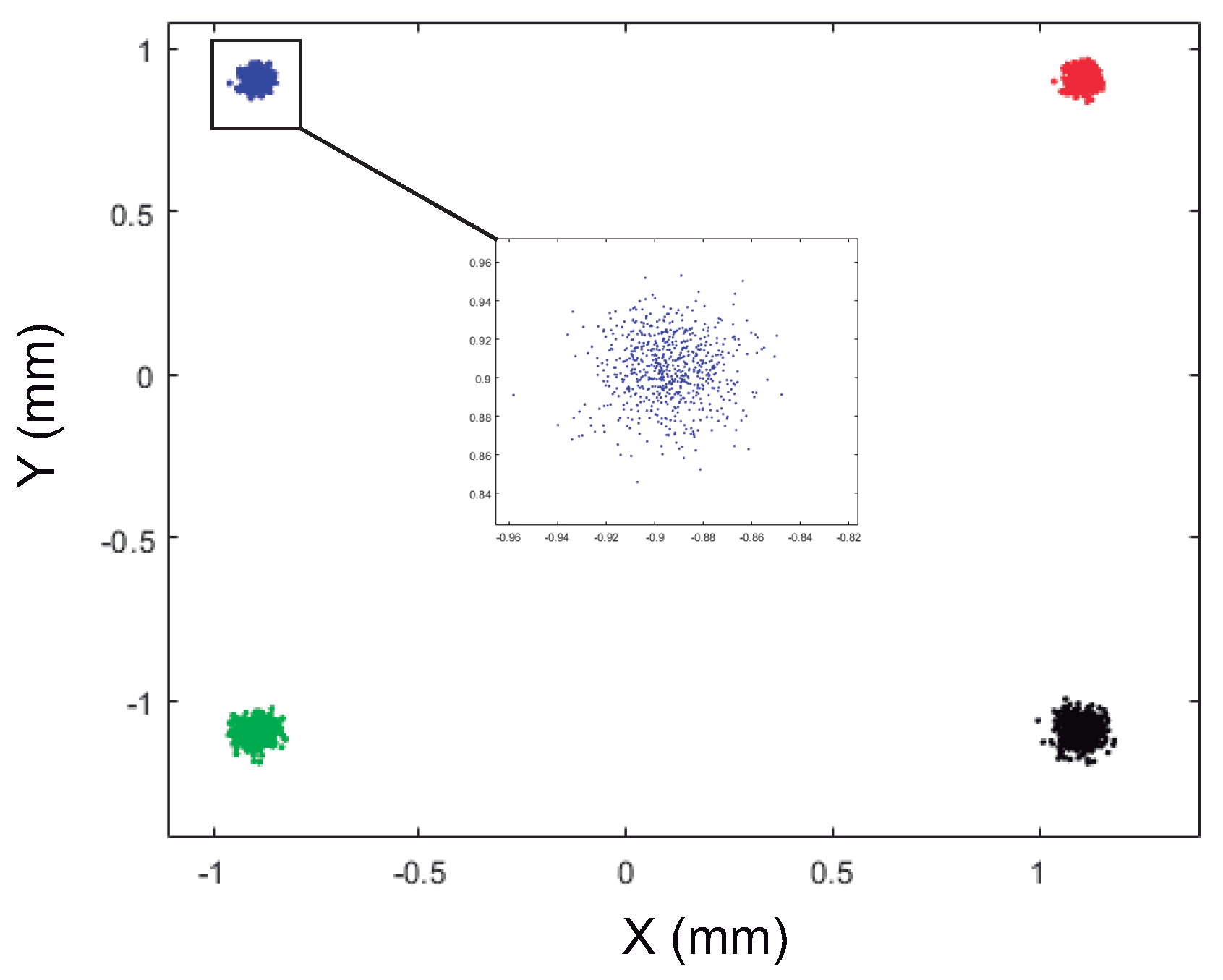
The different tests detailed below are carried out considering different numbers of samples and sampling frequencies. The first results obtained are from a test that considers 9000 samples. The process of calculating the point of impact of the different signals on the PSD surface is repeated 2000 times for each emitter in order to obtain reliable statistical results (Figure 18). The cloud of points with the worst stability is zoomed for a better visualization in Figure 18). The zoomed cloud of points illustrates correctly the problem that later is solved in the paper.
As can be seen in the enlargement of one of the areas in the Figure 18, the point cloud is not centred around a specific value, there are several areas of point concentration. This is due to the fact that in the calculation of the signal value for that frequency in the different channels, only one DFT value has been used, obtained through Goertzel’s algorithm. And since it is a discrete system, the noises can cause instabilities and part of the values that should coincide in a sample have been derived to the previous or subsequent one. Therefore, it will be necessary to process also the samples before and after the one corresponding to the searched frequency. A different scenario is proposed when making this proposal; now the algorithm would need to be processed in 48 times instead of 16. This makes impossible the use of high sampling frequencies that allow many measurements per second and acquire an optimus samples per cycle for DFT calcultion (Figure 19). This graph (as Figure 16) shows the sample frequency and number of samples that will be useful in parallel processing, where the CPU processes the data while the peripherals acquire the signals.
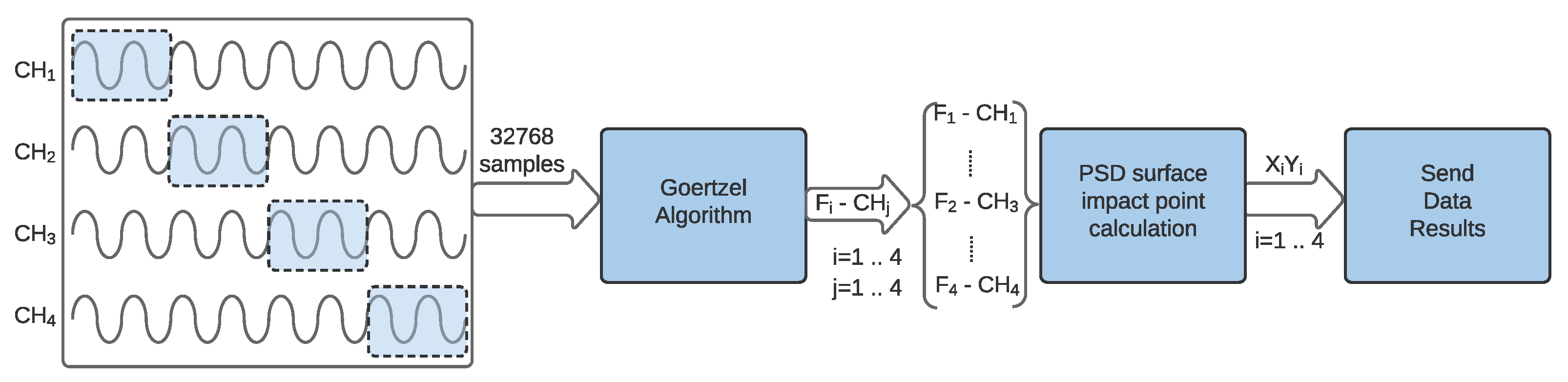
Therefore, it is decided to change the approach and perform a sequential execution obtaining samples and then processing them; and once the complete cycle is finished, launch the sample acquisition again, and so forth. This would allow to increase the sampling frequency, obtaining cleaner signals and favoring the accuracy of the algorithm. This execution process is detailed on Figure 20, where C H i correspond to the different output channels of the PSD and f i the frecuency of each emitter.
With this new proposal, the sampling frequency has been increased to 1.8 MHz. 8192 samples per channel are obtained (a total of 4 × 16,384 = 32,768 samples) in an acquisition time of approximately 19 ms. After the acquisition of samples, the process time is carried out obtaining the times shown in the 
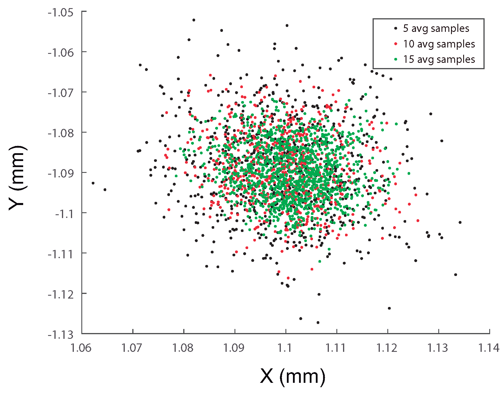
Table 5. To improve the determination of the positioning point it is decided to make an average of the last 5 points calculated.
Adding up the times obtained in the different phases of the process. The total time of the process is calculated, which is 66.8 ms. This time allows to get the position 15 times per second, which for the most common applications, where the speed of movement is not very high, is enough.
At this point, the tests are repeated considering the same scenario of the previously performed ones, and the results shown in the Figure 21 are obtained.
It can be seen that the point cloud is now centred on a single point, this result is more reliable despite having a greater dispersion.
The Table 6 shows the error of the value obtained from the centre of the point cloud with respect to the synthetic value entered. This error could be solved with an electrical calibration since they are systematic errors [20,21]. Concerning the random errors, the point cloud presents maximum deviations of the order of 50.0 μ m on the surface of the PSD. However, it can be seen in the Figure 21 that the majority of points are concentrated near the mean value, confirming this with the standard deviation values shown in the Table 7 which in no case exceed 30 μ m on the surface of the PSD.
These results should be extrapolated from the surface of the PSD, to space position results in the IPS with the Equation (6), which relates increases in (x,y) to increases in (X,Y).
( Δ x , Δ y ) f = ( Δ X , Δ Y ) H ,
where (X,Y) are the position in space and H the height at which the emitters are placed to the motion plane. In this way, it can be shown with the standard deviation that in 67% of the points the error of 3D emitter position, in the IPS covering an area of 3.5 × 3.5 m is less than 1.31 cm. This result could be improved by averaging results, making use of the previous Goertzel results, and introducing to the calculation of the position an average of the previous n 1 results and the current one. The viability of this solution will depend on the speed of the agent whose position is to be calculated. Performing this averaging, the results shown in the Table 8 and the Figure 22 are obtained. These values have been obtained for the 14 kHz emitter, which is the one with the worst results.
It is observed that the difference between making an average or not is significant. Not so much the number of measures used, since for 5 samples we obtain good error results, but the fact of making this improvement. Bearing in mind that, as we saw in the Table 5 it does not suppose a relevant increase in the computation time, it is of interest to evaluate the possibility of applying the averaging taking into account that in moving agents it can suppose an increase of the error, depending on the speed of the movement.
It is important to note that the errors described here are due only to the treatment and processing of the signals in a microcontroller. These errors should be added to the errors of the positioning system. The positioning system together with the positioning errors according to different parameters is shown in References [16,25]. In which you can see the errors in real environments under both static and dynamic conditions, obtaining positioning errors below 1 cm.
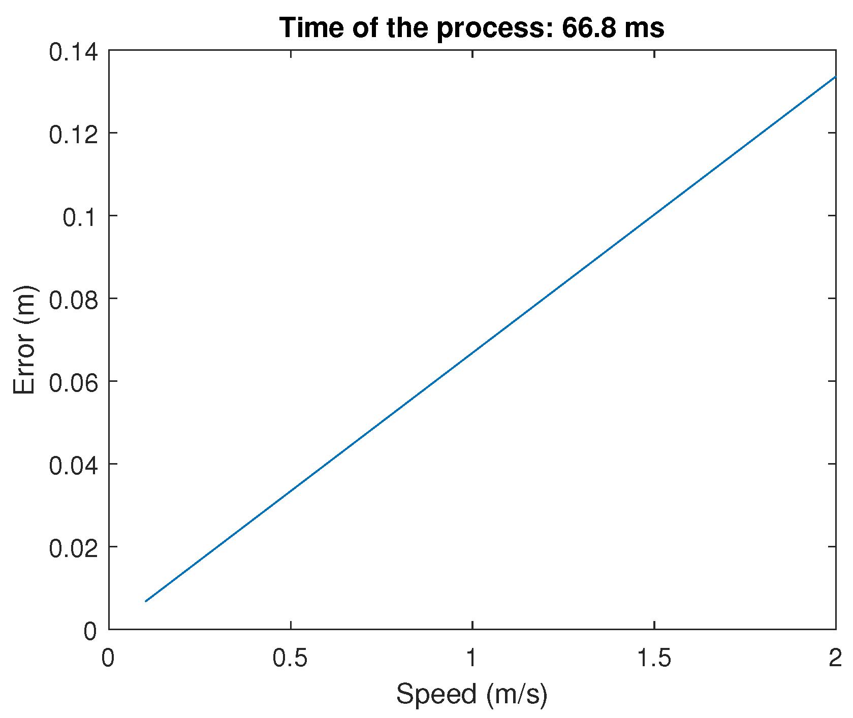
In addition to these errors, it is necessary to analyze the error of position determination in dynamic environments. Let us assume that the receiver is moving. As the execution time of the algorithm can not be considered zero, there will be an error in the determination of the position of the agent. Figure 23 shows the maximum error in positioning as a function of the mobile speed.
In the same way, an error will occur in the measurement of the rotation of the mobile depending on its angular speed.
Another aspect to consider is the focal length chosen for the lens system. The shorter the focal length, the greater the FoV and therefore the coverage. The further the emitter is from the receiver, the worse the SNR of the received signal in the receiver and therefore the measurement accuracy will worsen. In Reference [20] you can find information on how the SNR varies depending on—the focal length of the lenses, the distance between the transmitter and the receiver, the angle between them, and so forth.

5. Conclusions

In this paper we have presented the state of development of optical signal based IPS, developed in the GEINTRA group of the University Alcala considering the theoretical alternatives that exist to carry out the discrimination of different signals in situations of multiple access. The possibility of including the whole system, and the necessary processing for the development of IPS, in a MCU dispositive has been considered, reaching the initial conclusion that by using I/Q demodulators implies the implementation of two low-pass filters, two multiplications and a module calculation (for each demodulators). So, given the computation times required by these modules it was concluded that it is not viable.
Analyzing the alternative based on Band-pass Filters, and considering the high computation time to perform floating-point operations in an MCU, the possibility to reduce the processing time of this type of filter, using fixed-point data, has been studied. After this analysis it is observed that frequency response is considerably widened so that the noise bandwidth becomes greater, reducing the SNR. On the other hand, it is also observed that the filter area without attenuation is no longer flat.
Taking into account this premise, the maximum sample acquisition frequency that could be supported and time needed for the filtering have been calculated. The sampling frequency limited the samples per cycle to approximately 2, which is clearly insufficient to be able to calculate an RMS value with guarantees in a not too high time. Consequently, this implementation proposal was discarded.
In the preliminary analysis of DFT-Discrete Fourier Transform it was considered that the computation time they require can make it feasible. Working with this alternative allows to increase the sampling frequency, obtaining cleaner signals and favoring the accuracy of the algorithm. The sampling frequency has been increased to 1.8 MHz. After the acquisition of samples (8192 samples per channel) and performing the filtering process a total time of 66.8 ms was obtained. This time allows to get the position 15 times per second, which for the most common applications, where the speed of movement is not very high, is enough.
It can be concluded that the use of Goertzel’s algorithm for the calculation of the DFT in MCU, as a technique to perform the multiple access discrimination by means of FDMA is a viable solution that also provides a good solution as far as computation times are concerned.

Author Contributions

Conceptualization, B.R.-M., J.L.L.-G., A.G.-V. and Á.D.-L.-L.-C.; Data curation, B.R.-M.; Formal analysis, B.R.-M..; Funding acquisition, J.L.L.-G. and A.G.-V.; Investigation, B.R.-M. and Á.D.-L.-L.-C.; Methodology, B.R.-M., Á.D.-L.-L.-C. and J.L.L.-G.; Project administration, J.L.L.-G.; Resources, J.L.L.-G., A.G.-V., and I.B.-M.; Software, B.R.-M.; Supervision, J.L.L.-G. and A.G.-V.; Validation, B.R.-M.; Visualization, B.R.-M.; Writing—original draft, B.R.-M.; Writing—review and editing, B.R.-M., J.L.L.-G., A.G.-V. and Á.D.-L.-L.-C. All authors have read and agreed to the published version of the manuscript.

Acknowledgments

This research was supported by the Spanish Research Program through the Indoor and Delimited-Outdoor Positioning and Navigation Network (REPNIN+) (Ref.: TEC2017-90808-REDT). Borja Rubiano-Muriel thanks the European Social Fund and Sistema Nacional de Garantia Juvenil (Ref. PEJ2018-004019-A). Álvaro De-La-Llana-Calvo thanks the Formación del Profesorado Universitario (FPU) program of the Spanish Ministry of Education, Culture and Sport (Ref. BOE-A-2015-12849).

Conflicts of Interest

The authors declare no conflict of interest.

References

  1. Raper, J.; Gartner, G.; Karimi, H.; Rizos, C. A critical evaluation of location based services and their potential. J. Locat. Based Serv. 2007, 1, 5–45. [Google Scholar] [CrossRef]
  2. Brimicombe, A.; Li, C. Location-Based Services and Geo-Information Engineering; John Wiley & Sons: Hoboken, NJ, USA, 2009; Volume 21. [Google Scholar]
  3. Thoben, K.D.; Wiesner, S.; Wuest, T. “Industrie 4.0” and smart manufacturing-a review of research issues and application examples. Int. J. Autom. Technol. 2017, 11, 4–16. [Google Scholar] [CrossRef] [Green Version]
  4. Röwekämper, J.; Sprunk, C.; Tipaldi, G.D.; Stachniss, C.; Pfaff, P.; Burgard, W. On the position accuracy of mobile robot localization based on particle filters combined with scan matching. In Proceedings of the 2012 IEEE/RSJ International Conference on Intelligent Robots and Systems, Vilamoura, Portugal, 7–12 October 2012; pp. 3158–3164. [Google Scholar]
  5. Rashidi, P.; Mihailidis, A. A survey on ambient-assisted living tools for older adults. IEEE J. Biomed. Health Inform. 2012, 17, 579–590. [Google Scholar] [CrossRef] [PubMed]
  6. Hansen, R.; Wind, R.; Jensen, C.S.; Thomsen, B. Seamless indoor/outdoor positioning handover for location-based services in streamspin. In Proceedings of the 2009 Tenth International Conference on Mobile Data Management: Systems, Services and Middleware, Taipei, Taiwan, 18–20 May 2009; pp. 267–272. [Google Scholar]
  7. Calderoni, L.; Ferrara, M.; Franco, A.; Maio, D. Indoor localization in a hospital environment using random forest classifiers. Expert Syst. Appl. 2015, 42, 125–134. [Google Scholar] [CrossRef]
  8. Indoor Location Market by Positioning Systems, Maps and Navigation, Location Based Analytics, Location Based Services, Monitoring and Emergency Services. Worldwide Market Forecasts and Analysis. Markets&Markets, 2014–2019. Available online: https://www.marketsandmarkets.com/Market-Reports/indoor-location-market-989.html (accessed on 30 March 2020).
  9. Retail Indoor Location Market Breaks US Dollar 10 Billion in 2020; ABIresearch: Oyster Bay, NY, USA, 2015.
  10. Beliveau, Y.J.; Fithian, J.E.; Deisenroth, M.P. Autonomous vehicle navigation with real-time 3D laser based positioning for construction. Autom. Constr. 1996, 5, 261–272. [Google Scholar] [CrossRef]
  11. Weber, T.J. System and Method for Sonic Positioning. U.S. Patent 5,491,670, 13 February 1996. [Google Scholar]
  12. Kolodziej, K.W.; Hjelm, J. Local Positioning Systems: LBS Applications and Services; CRC Press: Boca Raton, FL, USA, 2006. [Google Scholar]
  13. Gu, X.; Ekambaram, V.K.; Ramani, A.; Yang, J.H.; Di Prizio, G.M.; Jones, C. Systems and Methods for High-Precision Indoor Positioning, Navigation and Shopping Behavior Profiling. U.S. Patent 8,930,134, 6 January 2015. [Google Scholar]
  14. Kim, J.; Jun, H. Vision-based location positioning using augmented reality for indoor navigation. IEEE Trans. Consum. Electron. 2008, 54, 954–962. [Google Scholar] [CrossRef]
  15. Priyantha, N.B. The Cricket Indoor Location System. Ph.D. Thesis, Massachusetts Institute of Technology, Boston, MA, USA, 2005. [Google Scholar]
  16. Rodríguez-Navarro, D.; Lázaro-Galilea, J.L.; De-La-Llana-Calvo, Á.; Bravo-Muñoz, I.; Gardel-Vicente, A.; Tsirigotis, G.; Iglesias-Miguel, J. Indoor positioning system based on a PSD detector, precise positioning of agents in motion using AoA techniques. Sensors 2017, 17, 2124. [Google Scholar] [CrossRef] [PubMed] [Green Version]
  17. Liu, M.; Wang, H.; Yang, Y.; Zhang, Y.; Ma, L.; Wang, N. Rfid 3-d indoor localization for tag and tag-free target based on interference. IEEE Trans. Instrum. Meas. 2018, 68, 3718–3732. [Google Scholar] [CrossRef]
  18. Seco, F.; Jiménez, A.R.; Peltola, P. A review of multidimensional scaling techniques for RSS-based WSN localization. In Proceedings of the 2018 International Conference on Indoor Positioning and Indoor Navigation (IPIN), Nantes, France, 24–27 September 2018; pp. 1–8. [Google Scholar]
  19. Mautz, R. Indoor Positioning Technologies; ETH Zurich: Zürich, Switzerland, 2012. [Google Scholar]
  20. Rodríguez-Navarro, D.; Lázaro-Galilea, J.L.; Bravo-Muñoz, I.; Gardel-Vicente, A.; Tsirigotis, G. Analysis and calibration of sources of electronic error in PSD sensor response. Sensors 2016, 16, 619. [Google Scholar] [CrossRef] [PubMed] [Green Version]
  21. Rodríguez-Navarro, D.; Lázaro-Galilea, J.L.; Bravo-Muñoz, I.; Gardel-Vicente, A.; Domingo-Perez, F.; Tsirigotis, G. Mathematical model and calibration procedure of a psd sensor used in local positioning systems. Sensors 2016, 16, 1484. [Google Scholar] [CrossRef] [PubMed] [Green Version]
  22. De-La-Llana-Calvo, Á.; Lázaro-Galilea, J.L.; Gardel-Vicente, A.; Rodríguez-Navarro, D.; Bravo-Muñoz, I.; Tsirigotis, G.; Iglesias-Miguel, J. Modeling infrared signal reflections to characterize indoor multipath propagation. Sensors 2017, 17, 847. [Google Scholar] [CrossRef] [PubMed] [Green Version]
  23. De-La-Llana-Calvo, Á.; Lázaro-Galilea, J.L.; Gardel-Vicente, A.; Rodríguez-Navarro, D.; Bravo-Muñoz, I.; Tsirigotis, G.; Iglesias-Miguel, J. Modeling the effect of optical signal multipath. Sensors 2017, 17, 2038. [Google Scholar] [CrossRef] [PubMed] [Green Version]
  24. De-La-Llana-Calvo, Á.; Lázaro-Galilea, J.L.; Gardel-Vicente, A.; Rodríguez-Navarro, D.; Bravo-Muñoz, I.; Espinosa-Zapata, F. Characterization of multipath effects in indoor positioning systems by AoA and PoA based on optical signals. Sensors 2019, 19, 917. [Google Scholar] [CrossRef] [PubMed] [Green Version]
  25. De-La-Llana-Calvo, Á.; Lázaro-Galilea, J.L.; Gardel-Vicente, A.; Rodríguez-Navarro, D.; Rubiano-Muriel, B.; Bravo-Muñoz, I. Analysis of Multiple-Access Discrimination Techniques for the Development of a PSD-Based VLP System. Sensors 2020, 20, 1717. [Google Scholar] [CrossRef] [PubMed] [Green Version]
  26. Yoshino, M.; Haruyama, S.; Nakagawa, M. High-accuracy positioning system using visible LED lights and image sensor. In Proceedings of the 2008 IEEE Radio and Wireless Symposium, Orlando, FL, USA, 22–24 January 2008; pp. 439–442. [Google Scholar]
  27. Nakazawa, Y.; Makino, H.; Nishimori, K.; Wakatsuki, D.; Komagata, H. Indoor positioning using a high-speed, fish-eye lens-equipped camera in visible light communication. In Proceedings of the International Conference on Indoor Positioning and Indoor Navigation, Montbeliard-Belfort, France, 28–31 October 2013; pp. 1–8. [Google Scholar]
  28. Huynh, P.; Yoo, M. VLC-based positioning system for an indoor environment using an image sensor and an accelerometer sensor. Sensors 2016, 16, 783. [Google Scholar] [CrossRef] [PubMed] [Green Version]
  29. Xu, Y.; Zhao, J.; Shi, J.; Chi, N. Reversed three-dimensional visible light indoor positioning utilizing annular receivers with multi-photodiodes. Sensors 2016, 16, 1254. [Google Scholar] [CrossRef] [PubMed] [Green Version]
  30. Sakai, N.; Zempo, K.; Mizutani, K.; Wakatsuki, N. Linear Positioning System based on IR Beacon and Angular Detection Photodiode Array. In Proceedings of the International Conference on Indoor Positioning and Indoor Navigation (IPIN), Alcalá de Henares, Spain, 4–7 October 2016. [Google Scholar]
  31. Dragūnas, K. Indoor multipath mitigation. In Proceedings of the 2010 International Conference on Indoor Positioning and Indoor Navigation, Zurich, Switzerland, 15–17 September 2010; pp. 1–7. [Google Scholar]
  32. De Lausnay, S.; De Strycker, L.; Goemaere, J.P.; Nauwelaers, B.; Stevens, N. A survey on multiple access Visible Light Positioning. In Proceedings of the 2016 IEEE International Conference on Emerging Technologies and Innovative Business Practices for the Transformation of Societies (EmergiTech), Balaclava, Mauritius, 3–6 August 2016; pp. 38–42. [Google Scholar]
  33. Oppenheim, A.V.; Schafer, R.W. Tratamiento de Señales en Tiempo Discreto; Person Education Inc.: London, UK, 2012. [Google Scholar]
Figure 1. Indoor Positioning System (IPS) Scheme.
Electronics 09 00782 g001
Figure 2. Equivalent circuitry of a pin-cushion Position Sensitive Devices (PSD) sensor (picture courtesy of Hamamatsu, obtained from the technical information of PSD).
Electronics 09 00782 g002
Figure 3. IQ Demulation flowchart.
Electronics 09 00782 g003
Figure 4. Band-Pass filters flowchart.
Electronics 09 00782 g004
Figure 5. Composite signal.
Electronics 09 00782 g005
Figure 6. Fast Fourier Transform (FFT) of composite signal.
Electronics 09 00782 g006
Figure 7. Zynq 7020.
Electronics 09 00782 g007
Figure 8. Flowchart of the IIR DirectForm-II.
Electronics 09 00782 g008
Figure 9. Frequency Response Floating Point IIR Filter—zoomed image.
Electronics 09 00782 g009
Figure 10. Frequency Response of IIR Filter implemented by 2 n integer IIR Filter—zoomed image.
Electronics 09 00782 g010
Figure 11. Goertzel Algorithm Flowchart.
Electronics 09 00782 g011
Figure 12. Detail of the microcontroller unit (MCU) used (L-Tek FF-LPC546xx).
Electronics 09 00782 g012
Figure 13. Conditioning circuit schematic.
Electronics 09 00782 g013
Figure 14. Detail of the Position Sensitive Devices (PSD) detector and conditioning board.
Electronics 09 00782 g014
Figure 15. IIR processing time and available time comparative.
Electronics 09 00782 g015
Figure 16. Goertzel’s algorithm processing time and available time comparative.
Electronics 09 00782 g016
Figure 17. Detail of the generated signals with the signal generator.
Electronics 09 00782 g017
Figure 18. Results on PSD surface.
Electronics 09 00782 g018
Figure 19. Goertzel’s algorithm processing time and available time comparative for 3 Goertzel values and data report time.
Electronics 09 00782 g019
Figure 20. Acquisition, processing and reporting flowchart.
Electronics 09 00782 g020
Figure 21. Results on PSD surface (3 Goertzel values).
Electronics 09 00782 g021
Figure 22. Results on PSD surface after average (3 Goertzel values).
Electronics 09 00782 g022
Figure 23. Maximum error in the determination of the position as a function of the mobile movement speed.
Electronics 09 00782 g023
Table 1. Parameters for the IIR Filter.
Fstop1Fpass1Fpass2Fstop2Astop1ApassAstop2
5000 Hz5900 Hz6100 Hz7000 Hz50 dB1 dB50 dB
7000 Hz7900 Hz8100 Hz9000 Hz50 dB1 dB50 dB
9000 Hz9900 Hz10,100 Hz11,000 Hz50 dB1 dB50 dB
13,000 Hz13,900 Hz14,100 Hz15,000 Hz50 dB1 dB50 dB
Table 2. Processing times for the different filter implementations.
Floating-PointInteger Coefficients
13.79 μ s2.15 μ s
Table 3. Goertzel’s algorithm processing time for different number of samples per channel.
Number of Samples20484096819216,384
Execution Time0.2114 ms0.4269 ms0.8532 ms1.7050 ms
Table 4. Synthetic position for each emitter.
Emitter Frecuency6 kHz8 kHz10 kHz14 kHz
Coordinates(−1,1)(1,1)(−1,−1)(1,−1)
Table 5. Execution time of the process for 32,768 samples at 1.8 MSamples/s (ms).
Acquisition TimeGoertzels Execution TimeAverage (5 Samples)3-D Emitter PositionSend Data
18.7744.730.00660.00243.6
Table 6. Error for each emitter (mm).
Emitter Frecuency6 kHz8 kHz10 kHz14 kHz
x Coordinate−0.89231.1077−0.89301.1011
y Coordinate0.90290.9054−1.0952−1.0900
x Error−0.1077−0.1077−0.1070−0.1011
y Error0.09710.09460.09520.0900
Table 7. Standard deviation for each emitter (mm).
Emitter Frecuency6 kHz8 kHz10 kHz14 kHz
Δ x STD0.01650.01740.02320.0272
Δ y STD0.01770.01990.02390.0286
Table 8. Standard deviation and error in IPS space depending of number of samples used for average calculation (mm).
Number of Samples on AverageWithout Average51015
Δ x STD0.02720.01040.00840.0076
Δ y STD0.02860.01050.00800.0070
Max error on 3D position of the emitter12.54.63.73.3

