2. The Closed Loop Switched-Capacitor Integrator
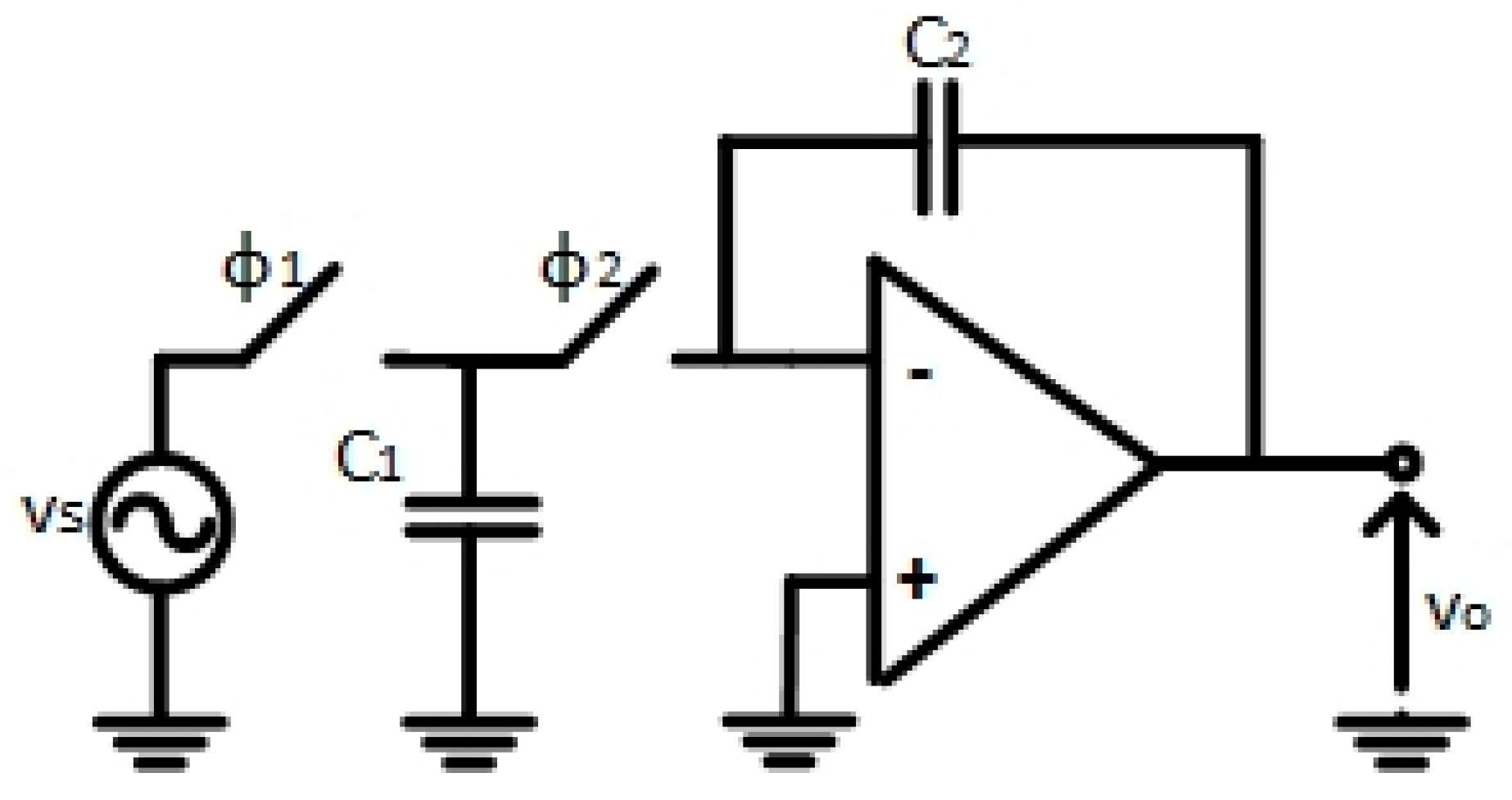
Figure 1 shows the conventional architecture of a switched capacitor integrator.
The switching scheme of this architecture is defined by two complementary clock phases,
ϕ1 and
ϕ2. During
ϕ1 phase, the input signal,
vs, is sampled with the input capacitor,
C1. During
ϕ2 phase the charge collected by
C1 is transferred to the feedback capacitor
C2, assuming an ideal virtual ground at the input of the OTA. The overall transfer function in Z-domain is the following
As in many other electronic systems, the feedback in this circuit serves two main functions:
- ▪
mitigate the impact of nonlinearities in the OTA;
- ▪
desensitize the overall transfer function to process, voltage, and temperature (PVT) variations.
The cost of these desirable features is an excessive OTA requirement.
2.1. Analysis of the Requirements of the Single Stage OTA
To evaluate the OTA requirements, a single-stage architecture was considered. The linear model of the OTA includes a transconductance
gm and an output resistance
ro.
Figure 2 reports the linear model of the integrator including the model of the OTA.
In a switched-capacitor integrator, the input signal,
vs, changes suddenly at each clock hit. Therefore,
vs can be assimilated to a step signal whose a maximum amplitude is equal to
Vi:
where
u(
t) is the unitary step signal.
The approach followed for this analysis is the following:
- 1
firstly, the transfer function is calculated;
- 2
the output voltage vo(s) is calculated in s domain multiplying the transfer function and the Laplace transform of vs(t);
- 3
vo(s) is then inverse transformed to get the output voltage, vo(t), in time domain.
The transfer function,
, is calculated as follows:
where
A0 (=
gm∙ro) is the OTA DC-gain. Assuming that both
ro and
gm tend to infinite,
can be approximate to the ideal value
:
The function
vs(
t) reported in Equation (2) is transformed in s domain and combined with Equation (3), and then the inverse Laplace Transform is evaluated as follows:
where
τp and
τz are time constants calculated as reciprocal of pole and zero of the transfer function, i.e.,
Assuming
,
τp can be approximated as follows:
The output voltage
vo(0) at
t = 0, is defined as:
The discontinuity is due to the zero in the transfer function.
2.2. Requirements of the Single Stage OTA
A finite gain of the OTA,
A0, and the non-null time is required for settling introduced errors on the output voltage. The OTA finite gain determines an error in a steady state. This error is called static error,
εstat:
On the base of Equations (4) and (5), the static error,
εstat, is calculated as follows:
where the last approximation is valid as
.
The charging process of the feedback capacitance,
C1, has a finite duration. In the following calculations, it is assumed that the duration of the charging phase is half of the clock period,
TCLK. Furthermore, an incomplete settling of the output voltage produces an error, which is called dynamic error,
εdyn, which is defined as follows:
By using the expression of
vo(
t), reported in Equation (5), the dynamic error,
εdyn, is calculated as follows:
which can be simplified combining Equation (12) with Equations (6) and (7) that:
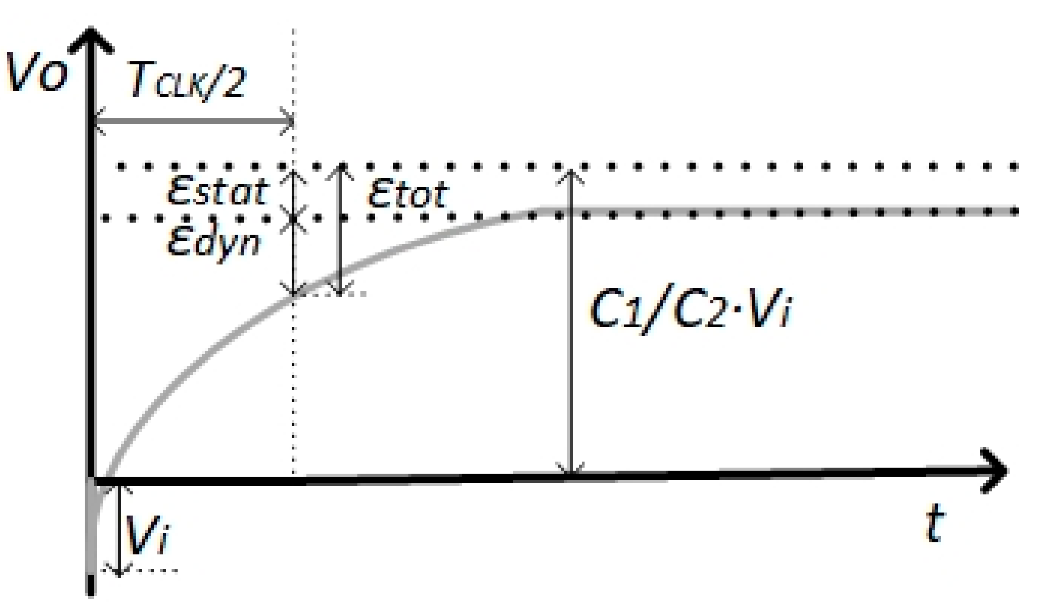
Figure 3 shows the qualitative behavior of the output voltage. Both static and dynamic errors are highlighted.
The overall error,
εtot, evalueated on the output voltage, is defined as the difference between the ideal output voltage,
C2/
C1∙Vi, and the output voltage measured at
TCLK/2:
As Equation (14) shows, εtot is calculated as the sum of εstat and εdyn.
2.2.1. DC-Gain Requirement of the Single-Stage OTA
The overall error must be less than the required accuracy, ξ, which is a parameter related to the application. According to the definition, both εstat and εdyn must be positive and smaller than the required accuracy, ξ.
To fulfill the DC-gain requirement, the accuracy of the static error,
εstat, needs to be addressed as follows:
Combining Equations (10) and (15), the following is obtained:
Then, the following constraint on the DC-gain,
Ao, is derived:
Since the DC-gain,
Ao, undergoes process, voltage and temperature variations, the sensitivity of
Ao,
, of the output voltage at
,
, is evaluated from Equation (5) as follows:
where last approximation is valid as
.
2.2.2. Transconductance Requirement of the Single Stage OTA
A transconductance constrain is determined through the relation between the accuracy specification and the dynamic error,
εdyn, i.e.:
Combining Equations (13) and (19), it is obtained:
The approximation contained in Equation (20) is justified as it is assumed that .
Combining Equations (7) and (20) the following constraint on
gm is set:
As for the DC-gain,
Ao, the sensitivity of the output voltage,
, at
,
, with respect to
gm is derived from Equation (5) as follows:
where the last approximation is valid as
and
.
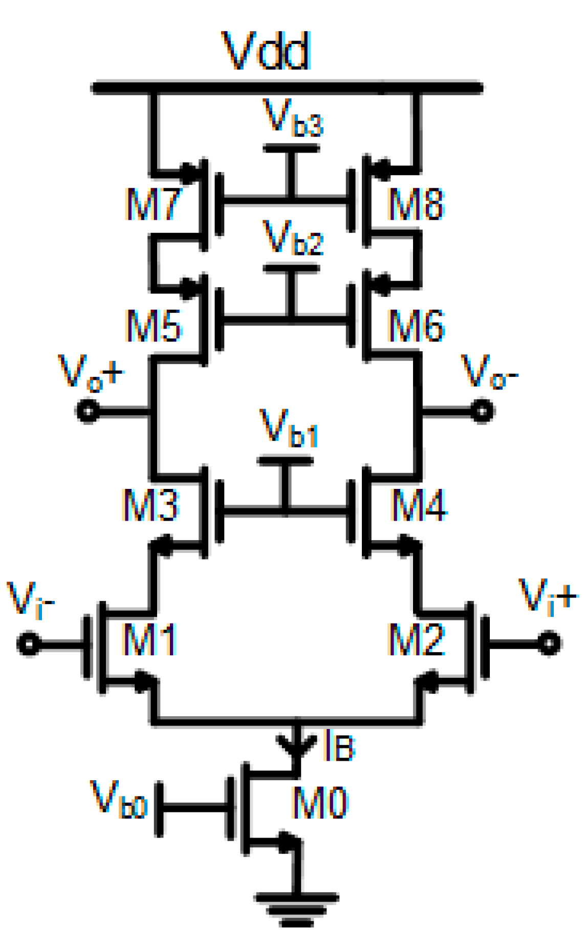
2.3. Circuit Implementation of the Single Stage OTA
A common circuit solution for the OTA is represented by the telescopic Cascode OTA, shown in
Figure 4 [
5,
6]. As the DC-gain requirement is satisfied and the output signal swing is sufficient, the telescopic Cascode OTA reported in
Figure 2 remains the most efficient and simplest OTA solution. Therefore, it was used as a benchmark in this paper.
The overdrive voltage of
M1-
M2 input transistors is limited by the available supply voltage,
Vdd, and the NMOS transistor threshold,
VTHN. Assuming a common mode,
Vcm, equal to
Vdd/2, by applying Kirchoff’s voltage law we obtain:
where
VGS1 is the gate-source voltage of
M1-
M2 input transistors, and
VDS0 is the drain-source voltage of the
M0 bias transistor.
The common mode,
Vcm, must assure that
M1-
M2 and the
M0 transistors work in the saturation region. Therefore, assuming that all the overdrives of
M1-
M2 and
M0 transistors are equal to
Vov, from Equation (23) we derive:
As seen in Equation (25), there is a strict limitation to the design of the overdrive of the input transistors at low supply voltage, which is typical of the modern CMOS IC technologies. For example, in finFET 16 nm technology, Vdd is 0.95 V, and VTHN is 0.275 V, therefore Vov must be less than 100 mV.
2.4. Small Signal Analysis of the Single-Stage OTA
The transconductance
gm of the linear model of
Figure 2 corresponds to the transconductance
gm1 of
M1-
M2 input transistors. The bias current,
IB, of the OTA is defined by the settling requirements, which mainly depends on
M1-
M2 input transistors.
The output resistance
ro of the linear model of
Figure 2 is calculated as follows:
where
gm3 and
gm5 are the transconductances of
M3 and
M5 transistors, respectively, and
ro1,
ro3, and
ro5 are the output resistances of
M1,
M2, and
M3 transistors, respectively. The last approximation in Equation (24) is valid assuming
gm3 ≅
gm5,
ro3 ≅
ro5, and
ro1 ≅
ro7. In practice, the output resistance of
M1-
M2 transistors,
ro1, is boosted by the intrinsic gain of transistor
M3,
gm3∙ro3.
The voltage gain,
A0, can be calculated as follows:
Rearranging Equation (27), we obtain:
where
VA3,
VA1,
Vov3, and
Vov1 are the early and the overdrive voltages of
M3 and
M1 transistors, respectively. As derived in Equation (28), the margins to increase the voltage gain
Ao are limited. A possibility to increment the voltage gain consists of reducing
Vov3 and
Vov1.
M3 and
M1 transistors are then pushed to work in the subthreshold region, where the transconductance depends only on the bias current, while the transistor overdrives approach their inferior limit of about 50 mV [
7]. Therefore,
Vov1 and
Vov3 have a strict range of variability between 50 mV and 100 mV.
VA3 and
VA1 can be increased by augmenting the length of
M3 and
M1. This solution degrades the frequency performance of the OTA since larger transistors introduce bigger parasitic capacitances. Moreover, every IC fabrication process has an intrinsic limit to the maximum allowable transistor length, which is lower and lower as the technology is scaled. For example, in FinFET 16 nm, the maximum allowable transistor length is 240 nm.
If the DC-gain requirement is not reachable by the telescopic Cascode OTA, it is necessary to modify the OTA architecture. An increment of
ro and, consequently,
Ao is obtained by using a regulated Cascode OTA [
8] or adding an output stage [
9]. Both previous solutions imply a significant increase in power consumption. It is also possible to increase the gain by augmenting the number of stacked transistors. At low voltage supply, the last solution is not practicable because of the further reduction of the output signal swing.
2.5. Slew-Rate (SR) Analysis of the Single-Stage OTA
Due to the finite bias current, IB, the OTA goes into a slew-rate regime at the beginning of the charging process.
According to Equation (5), the maximum rate of variation of the output voltage is obtained at
t = 0 s.
where
VSRi,max is the maximum amplitude of the input voltage step that keeps the OTA in the linear region. The corresponding output voltage in steady state is given by
VSRo,max, which is calculated as follows:
where the last approximation is valid as
A0 >> 1 +
C1/
C2. In a single-stage OTA, the slew-rate depends on the bias current
IB and the feedback capacitance
C2, i.e.:
where
gm1 and
Vov1 are the transconductance and the overdrive of the
M1-
M2 input transistors, respectively. Matching the
SR formula in Equation (31) to the maximum rate of variation of the output voltage reported in Equation (29), the
VSRo,max calculation is obtained:
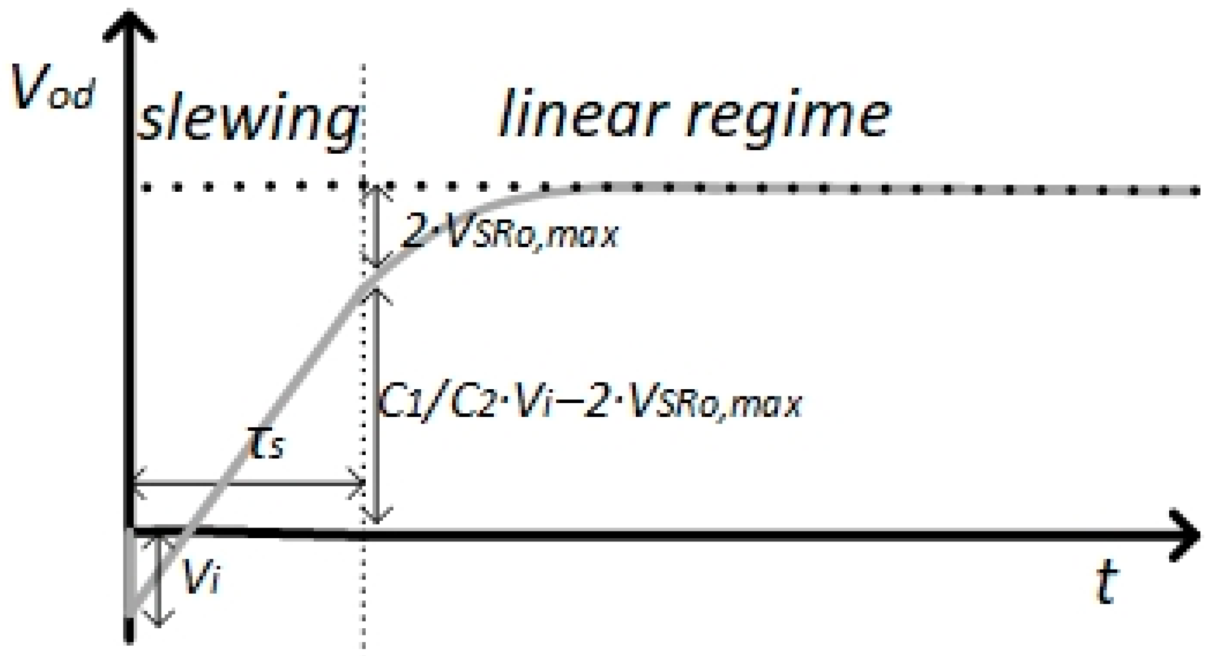
Due to its differential structure, the OTA starts slewing as the input differential voltage step,
Vi, overcomes 2∙
VSRi,max. The value of
VSRi,max is calculated by combining Equations (30) and (32):
The OTA slews until the output voltage reaches the value
:
where the starting value of
Vi depends on the fact that, at
t = 0 s, the capacitances of the integrator behave like short circuits, transferring the input voltage directly to the output.
From the previous equation, it is possible to calculate the slewing time of the OTA,
τs:
During
τs, the OTA output voltage evolves according to the linear law. Considering the slew-rate, the equation of the differential output voltage,
vod(
t), is then calculated as follows:
Figure 5 shows the step response of the closed loop switched capacitor integrator including the slewing period.
2.6. Signal to Noise (SNR) Calculations of the Closed-Loop Switched-Capacitor Integrator
The telescopic Cascode OTA suffers from a reduced output swing. Indeed, both single-ended output voltages must guarantee that the Cascode transistors (
M3-
M4 and
M5-
M6) work in a saturation region even under the signal swing. The main limitation is the negative output swing since three transistors are stacked between the ground and the output nodes, while only two transistors are stacked between
Vdd and the output nodes. Focusing the analysis on a single branch,
Vo+ must satisfy the following inequation to guarantee that
M3 transistors operate in saturation region:
where
VS3 and
VDS,sat3 are the source and the saturation voltages of
M3 transistor, respectively. It is assumed that
Vds,sat3 is equal to
Vov. The bias voltage
Vb1 is chosen to make
M1 transistor operating in saturation, i.e.:
where
VDS1,
VS1, and
VDS,sat1 are the drain-source, the source, and the saturation voltages of
M1 transistor, respectively. In this case, it is assumed that
Vds,sat1 is equal to
Vov.
VS1 is derived from the input transistor common mode,
Vcm, by dropping the gate-drain voltage of the
M1 transistors,
VGS1, i.e.:
Combining Equations (38) and (39) we obtain the minimum source voltage of
M3 transistor,
VS3,min:
By replacing
VS3 in Equation (37) with the value of
VS3,min calculated in Equation (40), the minimum value of
Vo+,
Vo+,min, is obtained:
As the output voltage starts swinging from the common-mode voltage,
Vcm, down to
Vo+,min, it is possible to calculate the maximum output voltage swing,
Vswing:
where the 2 factor is due to the differential architecture.
The thermal noise due to the switches around
C1 is calculated as
, where the coefficient 2 takes into account both the sampling (
ϕ1) and the integration phase (
ϕ2). Assuming that the thermal noise
is dominant, from Equation (42), the signal to noise ratio of the overall closed-loop switched-capacitor integrator,
SNRCL, is calculated as follows:
where
is the total output noise, as a result of the thermal noise contribution due to the
C1 switched-capacitor multiplied by the square of the integrator gain
, furthermore, the
factor takes into account that the input signal is a sinusoid.
2.7. Power Consumption Requirements
Regarding the telescopic Cascode shown in
Figure 4, the power consumption is given by the product of the supply voltage,
Vdd, and the bias current
IB:
Assuming dominant the thermal noise of
C1, the power consumption of the switched-capacitor integrator is determined by the settling time requirement. In fact, as the input transistor overdrive,
Vov1, is bonded to considerations on the DC-point at low voltage supply, the constraint on the input transistor transconductance,
gm1, expressed by in Equation (21), determines the minimum required bias current
IB,min:
Therefore, the minimum power consumption,
Pw,min, is obtained as follows:
As the OTA starts slewing, the minimum bias current,
IB,min, is determined by taking into account a different calculation for the dynamic error,
εdyn. Indeed, considering Equation (36) that assumes the slewing of the OTA, the differential output voltage at
is calculated as follows:
The dynamic error,
εdyn, is, then, calculated as follows:
Since
εdyn must be less than the required accuracy,
ξ, as reported in Equation (19), we obtain:
Moreover, the minimum bias current
IB,min is evaluated considering
τp reported in Equation (7), the transconductance of the input transistors,
gm1, determined as
, the formula of the slewing time,
τs, in Equation (35), and the previous equation. As a result the minimum bias current
IB,min, is calculated as follows:
The minimum power consumption,
Pw,min, is derived from the last equation as follows:
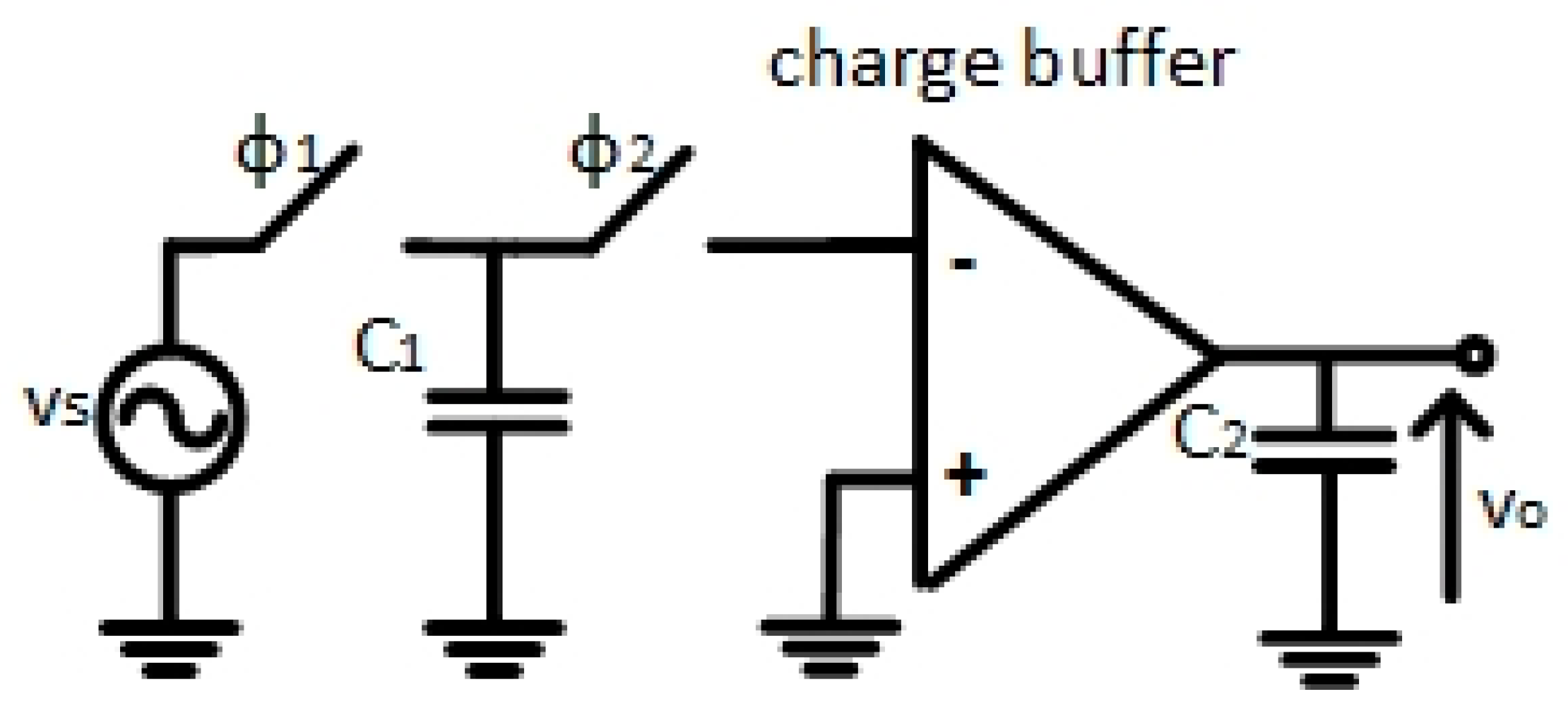
3. Proposed Open-Loop Integrator
As an alternative solution, an open-loop switched-capacitor integrator is presented (
Figure 6).
The active element is an OTA, with a low input impedance, which is called charge buffer. Once the input capacitance,
C1, is connected to the charge buffer input, it is discharged and its charge is transferred to the output capacitance
C2. The proposed open-loop switched-capacitor integrator does not include two input nodes with high and low impedances, unlike the switched-capacitor integrator based on a current conveyor [
10,
11], but only low impedance input nodes. Therefore, the voltage buffer used at the input in the conveyor integrators is eliminated. These simplifications help to get a more efficient circuit implementation.
According to the operation mode aforementioned,
C1 is connected to the inverting input terminal, it is possible to write:
where
Q1(
n−1) and
Q2(
n) are the charges stored in
C1 and
C2 capacitances, at
n − 1 and
n time steps, respectively. From Equation (52), it is obtained:
where
vo and
vs are the output and the input voltages. Therefore, it is possible to calculate the integrator gain in the Z domain,
:
By using the proposed approach, we obtain a gain expression, which is identical to the traditional closed-loop integrator reported in Equation (1). In both cases, the desensitization of the gain concerning the OTA parameters is reached as the gain depends only on the C1 and C2 capacitor ratio, in the ideal case.
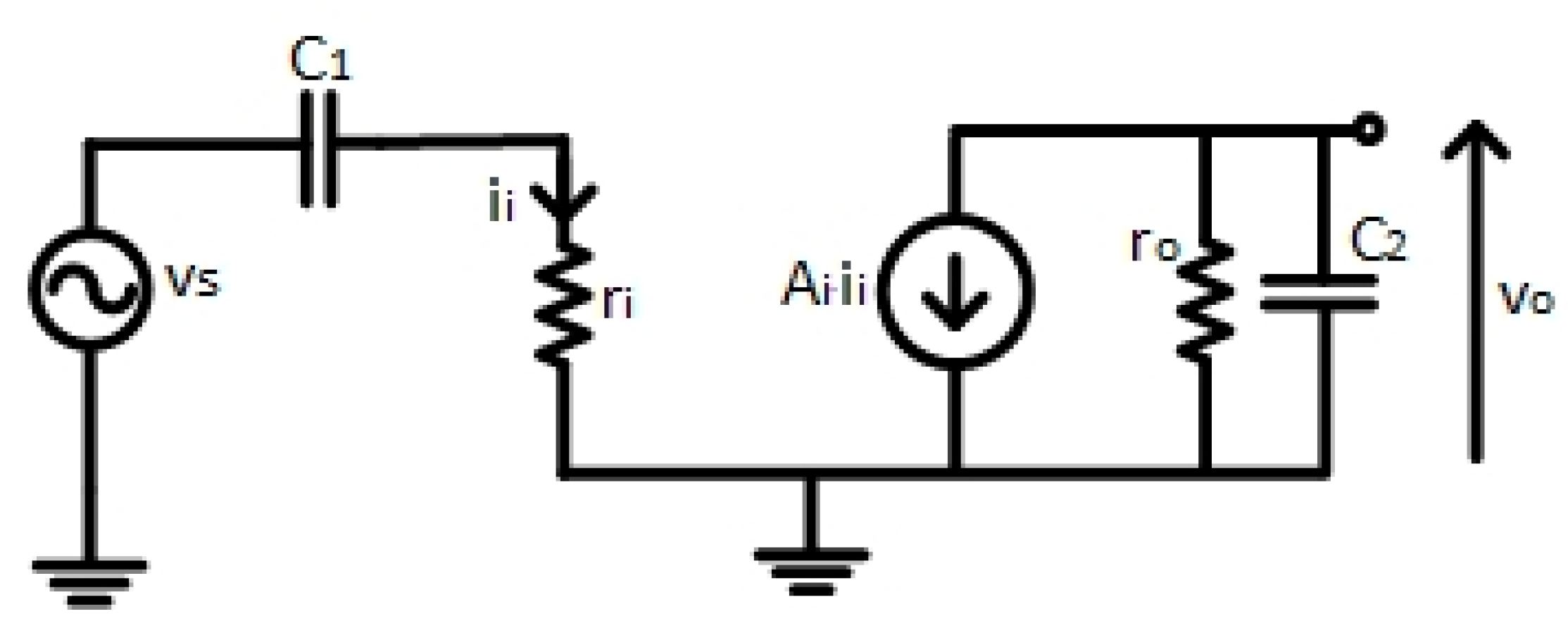
3.1. Small Signal Analysis of the Proposed Charge Buffer
To evaluate the impact of the non-null input resistance and the finite output resistance of the charge buffer, the linear model of the integrator reported in
Figure 7 was considered.
In practice, the C1 capacitance is discharged on input resistance ri, producing the input current ii. This current is amplified with a current gain Ai by the current amplifier that feds the output load made by the output resistance ro and the output capacitance C2.
First of all, the transfer function,
, is calculated as previously done for the traditional closed-loop switched-capacitor integrator:
Compared to the transfer function of the closed-loop switched-capacitor integrator shown in Equation (3), the transfer function of the open-loop switched-capacitor integrator already is calculated, has an additional pole due to the finite output resistance ro.
3.2. Transient Analysis of the Proposed Charge Buffer
Assuming a step signal at the input as reported in Equation (2), the output voltage becomes:
where:
Av is the voltage gain. The error on the current gain,
Ai, of the current mirror, directly affects the accuracy of the output voltage. This error mainly depends on the transistor mismatch, which can be minimized thanks to the appropriate design of the overdrive of the transistors forming the current mirror [
12].
The output resistance
ro, partially drags the charge stored in
C2. Considering a first-order Taylor’s expansion for the
e−t/τp2 term, and assuming a unitary current gain, the output voltage,
vo(
t), at
t = TCLK/2, is calculated as follows from Equation (56):
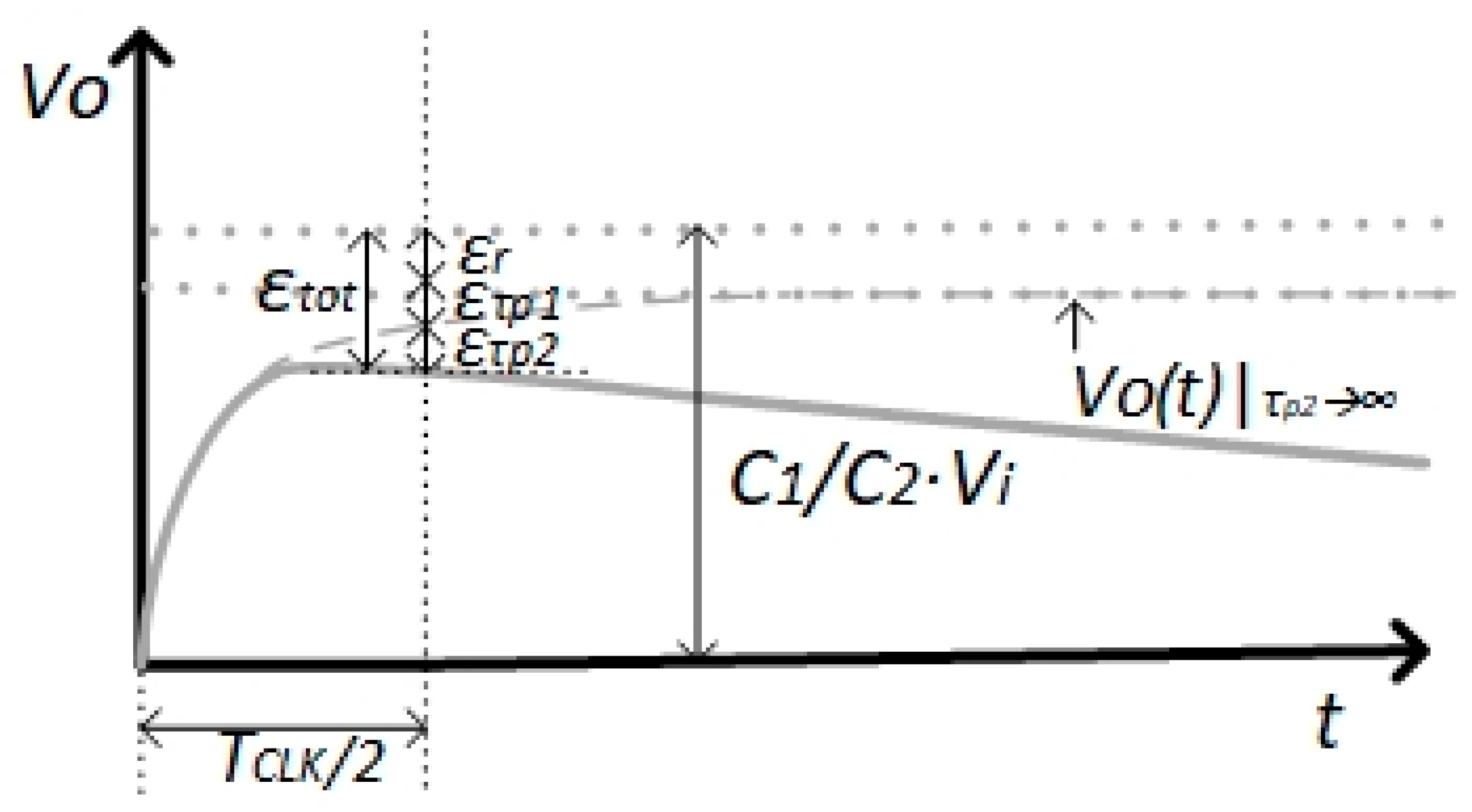
Three sources of error on the output voltage at , , remain. They are due to:
- ▪
finite voltage gain Av;
- ▪
non-null τp1;
- ▪
finite τp2.
The impact of each source of error is evaluated considering the remaining ones disabled.
To evaluate the error,
εr, due to the finite voltage gain,
Av, it is assumed that
τp1 tends to zero and
τp2 tends to infinite. In these conditions, the output voltage can be approximated as follows:
The corresponding error,
εr, is calculated as the difference between the ideal voltage obtained using the ideal gain value shown in Equation (54), and the value of the voltage expressed in Equation (59), i.e.,
To evaluate the error due to
τp1, it is assumed that
τp2 tends to infinite. In these conditions, the output voltage can be approximated as follows:
The error due to
τp1,
ετp1, is calculated as the difference between the output voltages expressed in Equations (50) and (52), i.e.:
The error due to
τp2,
ετp2, is calculated as the difference between the output voltages expressed in Equations (58) and (61), i.e.:
Figure 8 shows the output voltage behavior.
The sum of the three error
εr,
ετp1, and
ετp2, gives the total error
εtot, which must be less than the required accuracy,
ξ:
Since the error terms εr, ετp1, and ετp2 are positive, each of them must be less than ξ.
3.3. Voltage Gain Requirement of the Proposed Charge Buffer
As calculated in Equation (60),
εr is less than the
ξ, therefore, we obtain
In Equation (65) is very similar to Equation (17), which defines the requirement of the OTA for the closed-loop switched-capacitor integrator. It can be concluded that the charge buffer of the proposed open-loop switched-capacitor integrator requires the same gain of the OTA in the traditional closed-loop solution.
From Equation (58), the sensitivity,
, of the output voltage at
,
, and
Av is evaluated as follows:
where the last approximation is valid as
. The previous result is very similar to the one obtained for the Cascode OTA in the closed-loop switched-capacitor integrator in Equation (18).
3.4. Input and Output Resistances Requirements of the Proposed Charge Buffer
Assuming
ετp1, calculated in Equation (62), less than
ξ we obtain
Last approximation in Equation (67) is valid as .
Taking into account the expression of
τp1 in Equation (57), the following constraint on the input resistance,
ri, is obtained:
Assuming
ετp2, calculated in Equation (63), less than
ξ we obtain
In this case, last approximation is valid as .
Considering
τp2 in Equation (57), from Equation (69) it is derived the following constraint on the output resistance,
ro:
As already done for the voltage gain,
Av, from Equation (58) the sensitivity,
, of the output voltage at
,
, and
ri is evaluated as follows:
where last approximation is valid as
. This inequation is verified as the condition imposed by Equations (67) and (69) are satisfied, since, generally,
and
. It can be seen that the result of the calculation of the sensitivity of the output voltage compared to
ri is very similar to the one obtained for the calculation of the output voltage sensitivity for
gm of the Cascode OTA in the closed-loop switched-capacitor integrator in Equation (22).
Regarding the sensitivity, it can be concluded that the proposed switched-capacitor integrator, despite working in an open-loop configuration, has a robustness to PVT variations similar to the closed-loop switched-capacitor integrator.
However, since the performance of the proposed open-loop switched-capacitor integrator depends on the output resistance of the charge buffer,
ro, the sensitivity,
, of the output voltage at
,
, and
ro is calculated as:
According to Equation (69) and considering that and , it can be assumed that is quite less than 1. Therefore, the impact of the ro variation on the integrator performance is limited.
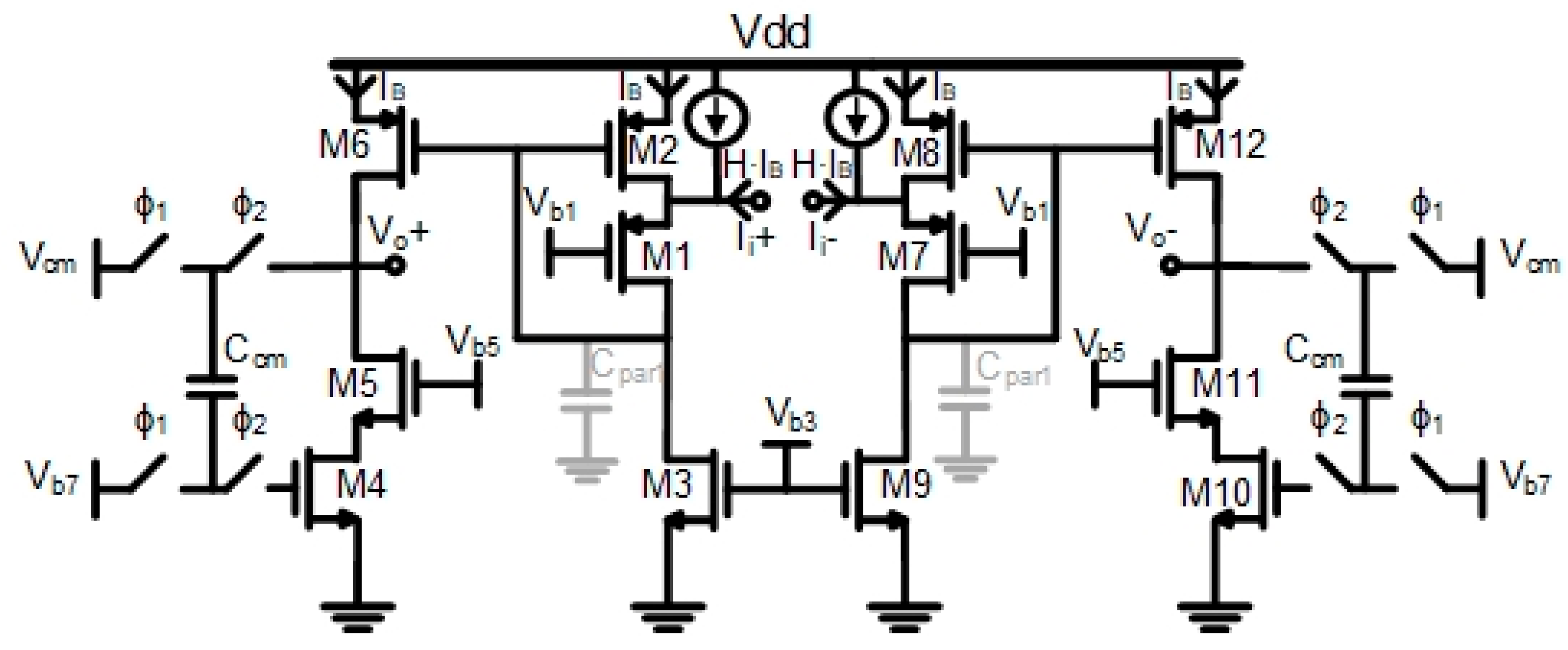
3.5. Circuit Implementation of the Proposed Charge Buffer
Figure 9 shows a possible circuit implementation of the charge buffer. The switched capacitors network at the output nodes is used to set the output common-mode voltage at
Vcm. Reference
Vb1 is designed to set the input common-mode voltage at
Vcm. To keep
M2 and
M8 transistors in the saturation region, their source-drain voltage must be more than their saturation voltage, i.e.:
It is supposed that
Vcm is equal to half supply voltage and the saturation voltages correspond to the transistor overdrive,
Vov2, from Equation (73) we derive
To bias the
M1 transistor in the saturation region, it must be guaranteed that its source-drain voltage,
VSD1, overcomes its saturation voltage, corresponding to the transistor overdrive,
Vov1, i.e.:
From the last equation, we obtain
Assuming
Vcm = Vdd/2, the last equation can be rearranged to obtain a constraint on the difference between the
M1 and
M2 transistors overdrives,
ΔVov2−1, i.e.:
Using the finFET 16 nm we obtain the result Vdd = 0.95 V, VTHP = 0.4 V. Consequently, ΔVov2−1 must be higher than 75 mV.
According to Equations (74) and (77), using a charge buffer in open-loop configuration gives more flexibility to the design since larger overdrives can be defined for the transistors, to employing an OTA in a closed-loop fashion. This is extremely important at low voltage supply.
The input and the output resistances,
ri and
ro, are calculated as follows:
where
gm1 and
gm2 are the transconductance of
M1 and
M2 transistors, respectively, while
rds3 and
rds6 are the output resistance of
M3 and
M6 transistors, respectively.
The voltage gain,
Av, is calculated as follows:
The telescopic Cascode OTA reported in
Figure 4 implements the boost of the output resistance,
ro. On the other end, the proposed charge buffer circuit enables the boosting of the transconductance of the input transistors,
gm1, by a
gm2∙
rds3 factor, lowering the input resistance,
ri. The impact on the final voltage gain is similar as demonstrated by the similitude of the voltage gain expressions reported in Equations (79) and (27), even if the voltage gain,
Av, of the proposed charge buffer results the double with respect to the telescopic Cascode OTA.
In both cases, the power consumption is determined by the settling requirements, i.e., both the time constants τp and τp1 for the closed-loop and the proposed open-loop switched-capacitor integrator, respectively. The time constant, τp, depends on 1/gm1. In this case, the only possibility to increase gm1 is to increase the bias current IB of the telescopic Cascode OTA, since the input transistor overdrive is bound to bias constraints. For the proposed integrator, the time constant τp1 is proportional to ri. However, in the last case, as the boost on the input transistor transconductance lowers the input resistance, ri, a significant power saving is obtained.
3.6. Slew-Rate Analysis of the Proposed Charge Buffer
According to Equation (56), the maximum rate of variation of the output voltage, i.e., the slew-rate, is obtained at the initial instant,
t = 0 s:
where:
The last approximation in Equation (81) is valid assuming .
The slew-rate depends on the bias current
IB and the output capacitance
C2, i.e.:
where
IB is the bias current of each branches composing the charge buffer drawn in
Figure 9.
Combining Equations (80) and (82) and considering the expression of
τp1 and
ri reported in Equations (57) and (78), respectively, we derive:
where
Vov1 and
Vov2 are the overdrive voltage of
M1 and
M2 transistors, respectively, and
VA3 is the early voltage of
M3 transistor.
Combining Equations (81) and (84), the value of
VSRi,max is obtained:
The output voltage range where the charge buffer operates in the linear regime, VSRo,max, has been reduced by a factor equal to concerning the traditional closed-loop switched-capacitor integrator with the OTA.
Due to its differential structure, the charge buffer starts slewing as
Vi > 2∙VSRi,max. If a slewing period is considered, the differential output voltage,
vod(
t), can be calculated as follows:
where
τs is the duration of the slewing period. The charge buffer slews until the output differential voltage,
vod(
t), is less than 2·
VSRo,max concerning the final value in steady-state, neglecting the losses due to the output resistance (i.e.,
τp2→∞):
From the combination of the last equation and Equation (83), the expression of
τs is derived:
3.7. SNR Analysis of the Proposed Open-Loop Switched-Capacitor Integrator
By focusing the analysis on a single branch,
Vo+ must satisfy the following inequation to guarantee that
M4 transistors operate in saturation region:
where
VS4 and
VDS,sat4 are the source and the saturation voltages of
M4 transistor, respectively. It is assumed that
Vds,sat4 is equal to
Vov. The bias voltage
Vb5 was chosen to make
M5 transistor operating in saturation, i.e.,
where
VDS5, and
VDS,sat5 are the drain-source, and the saturation voltages of
M4 transistor, respectively. In this case, it is assumed that
Vds,sat1 is equal to
Vov.
VS1 is derived from the
Vb5 bias voltage, by dropping the gate-drain voltage of the
M4 transistors,
VGS4, i.e.:
Vb1 can be designed to make
VS4, and, hence,
VDS5 equal to
VDS5,sat, i.e.,
Vov. If so, from Equation (88) we derive the minimum output voltage,
Vo+,min:
As the output voltage starts swinging from the common-mode voltage,
Vcm, down to
Vo,min, it is possible to calculate the maximum output voltage swing,
Vswing:
where the 2 factor is due to the differential architecture. It is assumed that
Vcm is equal to half
Vdd.
Assuming that the thermal noise due to the switches around
C1,
is dominant, from Equation (92), the signal to noise ratio of the overall open loop switched capacitor integrator,
SNROL, is calculated as follows:
where
is the total output noise, which is given by the thermal noise contribution due to the
C1 switched-capacitor multiplied by the square of the integrator gain
, and the
factor takes into account that the input signal is a sinusoid.
The resulting SNROL is slightly higher than the SNRCL calculated by Equation (43). The output noise is about the same since the noise contribution of C1 is assumed dominant. However, assuming VTH = 0.275 V and Vdd = 0.95 V as for the finFET technology and Vov = 0.1 V, due to bias constraint as defined by Equation (43), the output voltage swing for the proposed switched-capacitor integrator is higher.
3.8. Power Consumption Requirement of the Proposed Charge Buffer
The minimum power consumption,
Pw,min, is given by the product of the supply voltage
Vdd, by the minimum total bias current
IBTOT.min:
where
IB,min is the minimum
IB bias current. The power requirement is calculated according to the settling time requirement. In practice, the minimum bias current
IB,min is derived assuming that the
ετp1 error must be less than the required accuracy
ξ, i.e.:
As
Vi < 2·VSRi,max, the charge buffer is in the linear regime, where the expression of
IB,min is derived from Equation (62):
Combining Equations (94) and (96), the minimum required power consumption,
Pw,min, is calculated as follows:
As
Vi > 2∙VSRi,max, the charge buffer starts slewing. Considering the expression of the differential output voltage
vod(
t), including the slewing period reported in Equation (85), the calculation of the error due to
τp1,
ετp1, is updated as follows:
Considering
ετp1 as reported in the previous equation, the constraint on
τp1 is derived from Equation (95):
Looking at
τp1 and
ri in Equations (57) and (78), respectively, the minimum bias current that satisfies Equation (99),
IB,min is calculated as follows:
Combining Equations (97) and (100), the minimum required power consumption is calculated as follows:
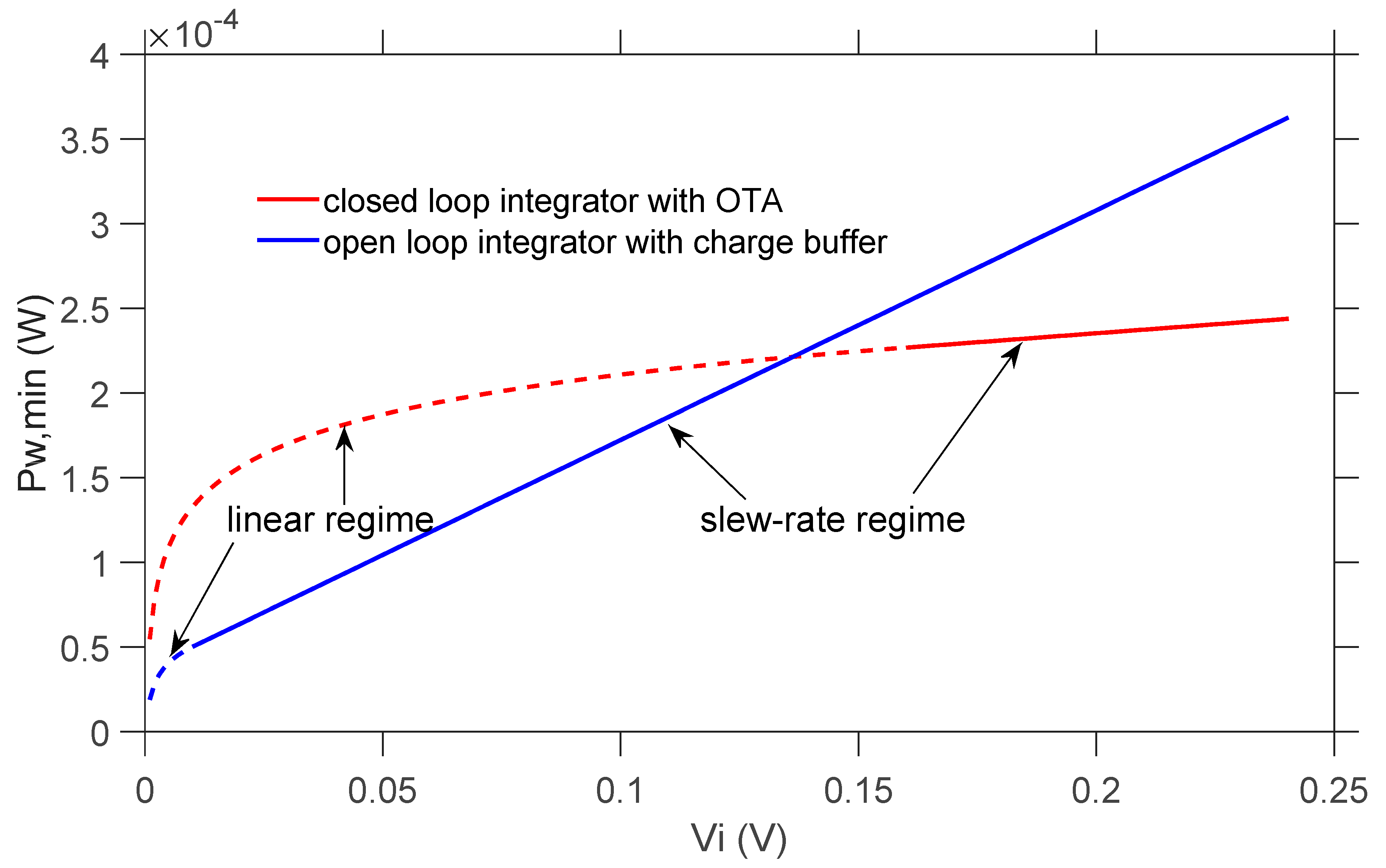
Figure 10 shows the power consumption of the proposed switched-capacitor integrator and the closed-loop switched-capacitor integrator plotted as a function of
Vi.
The two curves in
Figure 10 are obtained plotting the Equations (97) and (101) for the proposed design, and Equations (46) and (51) for the closed-loop switched-capacitor integrator. The common design parameters are reported in
Table 1.
The transistors overdrives have been defined according to the constraints derived from Equations (25), (74), and (77). The values of Cpar1, VA3, and VA6 are estimated from the simulation results. The H factor was set to 2 for the proposed design.
The minimum power required by the closed-loop switched-capacitor integrator is higher than the proposed open loop integrator for an input signal up to 140 mV large. For Vi = 31.25 mV, the proposed circuit requires a minimum power of 76 µW, while the closed-loop switched-capacitor integrator requires about 173 µW, i.e., more than the double.
3.9. Small Signal Analysis of the Charge Buffer Considering the Parasitic Capacitance Cpar1
The small-signal equivalent circuit shown in
Figure 7 is a first-order approximation of the small-signal behavior of the proposed transistor-level open-loop switched-capacitor integrator. Considering also the
Cpar1 as a parasitic capacitance shown in
Figure 9, a more accurate transfer function is obtained:
where
rds3 is the output resistances of
M3 transistor. The parasitic capacitance,
Cpar1, mainly depends on the gate capacitances of
M2 and
M6 transistors. Therefore, it can be approximated as follows:
where
W2 and
L2, and
W6 and
L6, are the width and the length of
M2 and
M6 transistors.
Concerning the transfer function reported in Equation (55), the transfer function in Equation (84) includes a further zero,
z1:
This zero is considered to be at a very high frequency and it does not produce significant effects on the step response of the proposed circuit.
Moreover, two complex poles appear in the transfer function. Their frequency,
ωo, and quality factor,
Q, are calculated as follows:
A high
Q factor determines a large overshoot,
OS, on the step response of the proposed circuit, and wide oscillations, which can have a severe impact on the accuracy of the output voltage. Otherwise, as the circuit is excessively dumped, the step response slows significantly. The criterion here adopted is to limit the overshoot to the required accuracy,
ξ, i.e.:
The previous equation is valid in linear regime; otherwise, in case of slewing of the charge buffer, the overshot is calculated as follows:
For the proposed design, the last equation is satisfied for a Q value of about to 0.75. The Q factor can be reduced by operating on Vov2 and Vov1, or, by acting on the H factor, which gives a further degree of freedom to the design.
The desired value of Q is reached by designing an H factor of 2.
4. Simulation Results
A transistor-level design of the proposed switched-capacitor circuit was performed in finFET 16 nm CMOS technology. The design parameter reported in
Table 1 were considered. The input signal,
Vi, was assumed equal to 31.25 mV. The bias current,
IB, set to 10 µA, corresponds to the minimum value,
IB,min, as predicted by Equation (100). The
H factor was set to 2 as derived from Equation (107). The minimum power consumption of the core circuit was 76 µA, as predicted by Equation (83).
According to Equation (65), the required voltage gain is 56 dB, while a voltage gain of 71 dB results from simulations. Similarly, the required output resistance obtained from Equation (70) was 1.4 MΩ, while the value obtained through simulations was 1.85 MΩ. Therefore, we can conclude that the voltage gain and the output resistance requirements were largely satisfied.
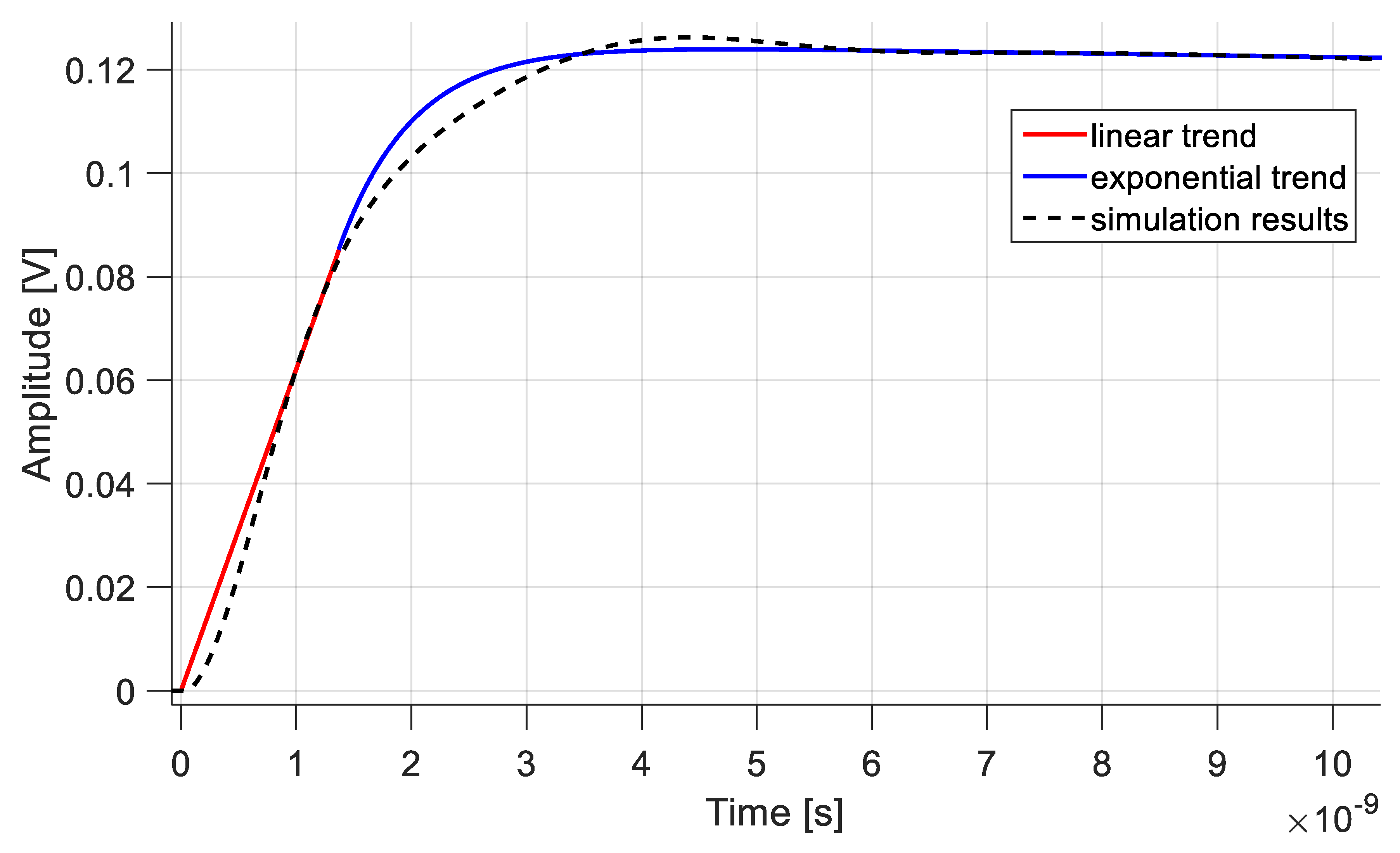
Figure 11 shows the response of the circuit to an input step of 31.25 mV for the theoretical model and simulations. The two curves are very close, proving the validity of the proposed circuit model. Based on the design parameters, the expected error on the output voltage at
TCLK/2 was 1 mV. This results from both the model prediction and the simulations.
The simulation results show a slightly marked overshot due to the complex poles generated by the internal loop including M1 and M2 transistors, as predicted in paragraph 3.9. However, the first-order model gives a valid approximation of the circuit behavior especially in the steady-state regime.
Table 2 summarizes the required values of the design parameters and their values obtained through simulations.
Table 3 reports the performance summary of the proposed switched-capacitor integrator and compares it to the state-of-the-art approach. The following figure of merit (
FoM) is introduced for a fast comparison
where
N is the number of poles of the switched-capacitor filter under consideration,
Pw is its power,
fCLK is the clock frequency and
OSR is the oversampling ratio, i.e., the ratio between half clock frequency and the maximum signal bandwidth.
As can be seen in
Table 3, the proposed work is well compared to the state of the art in terms of
FoM.


