Article

Sinusoidal Oscillators Operating at Frequencies Exceeding Unity-Gain Bandwidth of Operational Amplifiers

1
Department of Electronics, Robotics, Monitoring and IoT Technologies, National Aviation University, 03058 Kyiv, Ukraine
2
Projects and Maintenance Section, The Private Department of the President of the United Arab Emirates, Abu Dhabi 000372, UAE
*
Author to whom correspondence should be addressed.
Electronics 2020, 9(5), 845; https://doi.org/10.3390/electronics9050845
Submission received: 26 April 2020 / Revised: 13 May 2020 / Accepted: 17 May 2020 / Published: 20 May 2020
(This article belongs to the Special Issue Filter Design Solutions for RF systems)

Abstract

:
This paper proposes a novel operational amplifier (OPA) voltage-controlled oscillator (VCO) circuits on the basis of impedance converters. The VCO can operate over a frequency range exceeding unity-gain bandwidth due to the location of the tank circuit, not at the output of the OPA, but at the noninverting input. The paper presents the mathematical modeling of oscillated amplitude and start-up conditions. The simulation results confirm the theoretical achievements. The designed and simulated VCO uses an ultra-low noise wideband OPA LMH6629MF, covers a frequency band between 0.830 GHz and 1.429 GHz, and exhibits a maximum in-band total harmonic distortion (THD) of 1.7%. It has a maximum in-band phase noise of −139.3 dBc/Hz at 100 kHz offset frequency and has an outstanding value of a standard figure of merit (FoM) of −198.6 dBc/Hz. The zero-peak amplitude of output voltage is from 3.2 V to 4 V for all generated frequencies at a supply voltage of ±5 V. The fabricated prototype-oscillator based on OPA LMH6624 operates at a frequency of 583.1 MHz with a power level of 0 dBm.

1. Introduction

Sinusoidal oscillators are used in almost all systems of receiving and transmitting information, as well as in measuring instruments and systems. One of the most rapidly developing class of sinusoidal oscillators is the class of the voltage-controlled oscillator (VCO). Voltage-controlled oscillators are commonly used in digital frequency synthesizers, which are one of the main subsystems of modern communications systems. The rapid development of modern communications and instrumentation systems has created a high demand for low noise VCOs [1,2,3]. Modern microwaves sinusoidal oscillators use bipolar junction transistors (BJT), heterojunction bipolar transistors (HBT), a low-noise high-electron-mobility-transistors (HEMT) and pseudomorphic HEMT (pHEMT) as active devices for achieving low phase-noise performance [4,5,6]. The appearance on the market of a ultra-low-noise, high-speed, broadband operational amplifier (OPA) creates the possibility of their use in the sinusoidal oscillators in the ultra-high frequency range. For example, the LMH6629MF (Texas Instruments) OPA has an input noise voltage of 0.69 nV/√Hz at the corner frequency of 4 kHz, a slew rate of 1600 V/μs and small-signal −3 dB bandwidth of 900 MHz [7]. Low-noise, high-speed OPA oscillators can offer a practical alternative to transistor oscillators, the performance of which to some extent depends on the variability of the transistor small-signal parameters. The use of a low-noise, high-speed OPA as an active device in the oscillator circuits has some advantages [8,9]. An operational amplifier is an amplifier with very high input impedance and very low output impedance; it is easy to introduce required positive feedback around the OPA; the oscillator design is simple due to the lack of the bias circuit; the oscillator circuit does not require any adjustment during fabrication.
As is well known [8,10,11], oscillators based on the Colpitts and Hartley topology require a relatively high voltage gain to start-up oscillation. High voltage gains reduce the maximum frequency of oscillation because of the limited gain-bandwidth product of OPA. Besides, the maximum frequency of generated sinusoidal oscillations at the output of the OPA in the Colpitts and Hartley topologies is limited by the ratio of the slew rate to the amplitude of voltage oscillations multiplied by two pi [12]. Thus, with the required voltage amplitude of, say, three volts, and the use of the LMH6629 OPA, the maximum achievable frequency will be less than 85 MHz, which is very far from the microwave frequency range. By simple calculations, we can estimate what should be the slew rate of an OPA to achieve a frequency of 1 GHz with a 3 V amplitude of oscillations. It should be about 19,000 V/μs. Currently, such a slew rate in OPA is unattainable.
The VCO topology proposed in [13] uses the OPA circuit with negative input inductance observed at the noninverting input of the OPA. The disadvantage of this circuit is the use of two resistors, one of which presents the positive feedback circuit, and the second connects the inverting input of the OPA to the ground. These resistors are the source of thermal noise.
In this study, we propose several new VCO topologies that use the idea of a negative impedance converter. However, unlike the well-known studies [14,15,16,17], the converter circuit does not include resistors. In contrary to the Colpitts and Hartley oscillators requiring a sufficiently high voltage gain for self-excitation, the proposed oscillator circuits operate with a voltage gain of less than unity; this feature significantly increases the operating frequency, which can exceed the unity-gain bandwidth of the OPA. This particularity of the proposed VCO circuits is due to the location of the tank circuit not at the output of the OPA, but at the noninverting input. Mathematical modeling, simulation, and prototype implementation of the proposed oscillators are given.

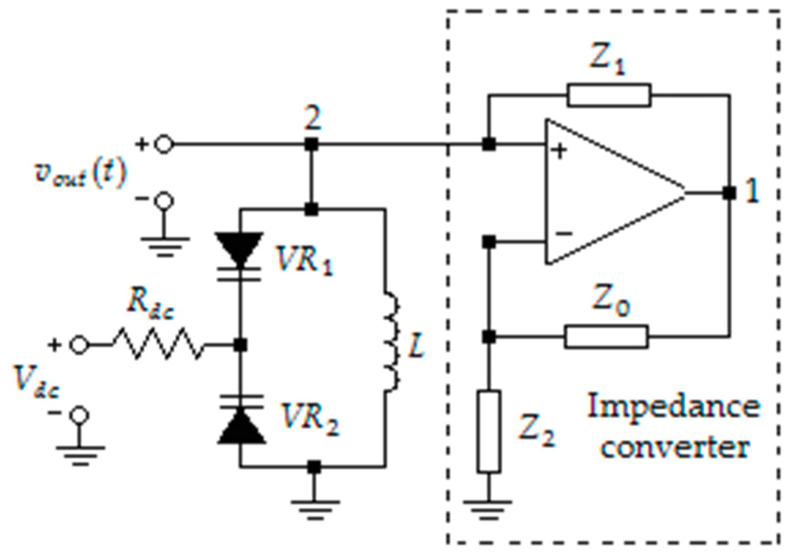
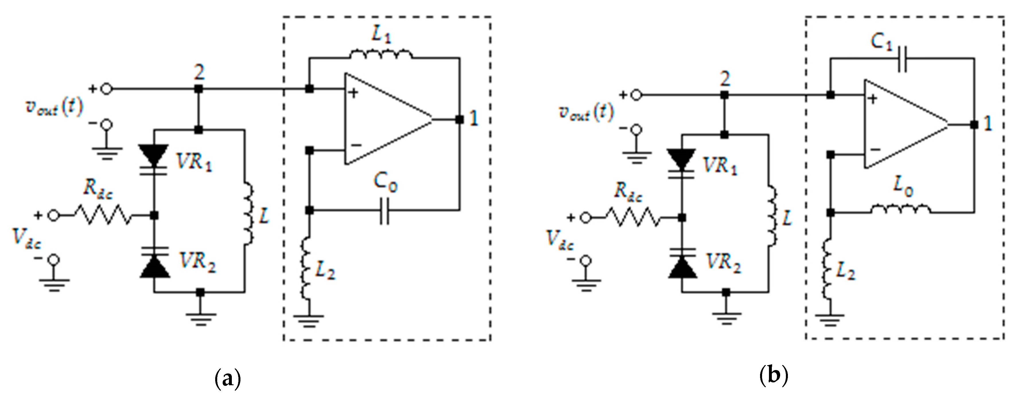
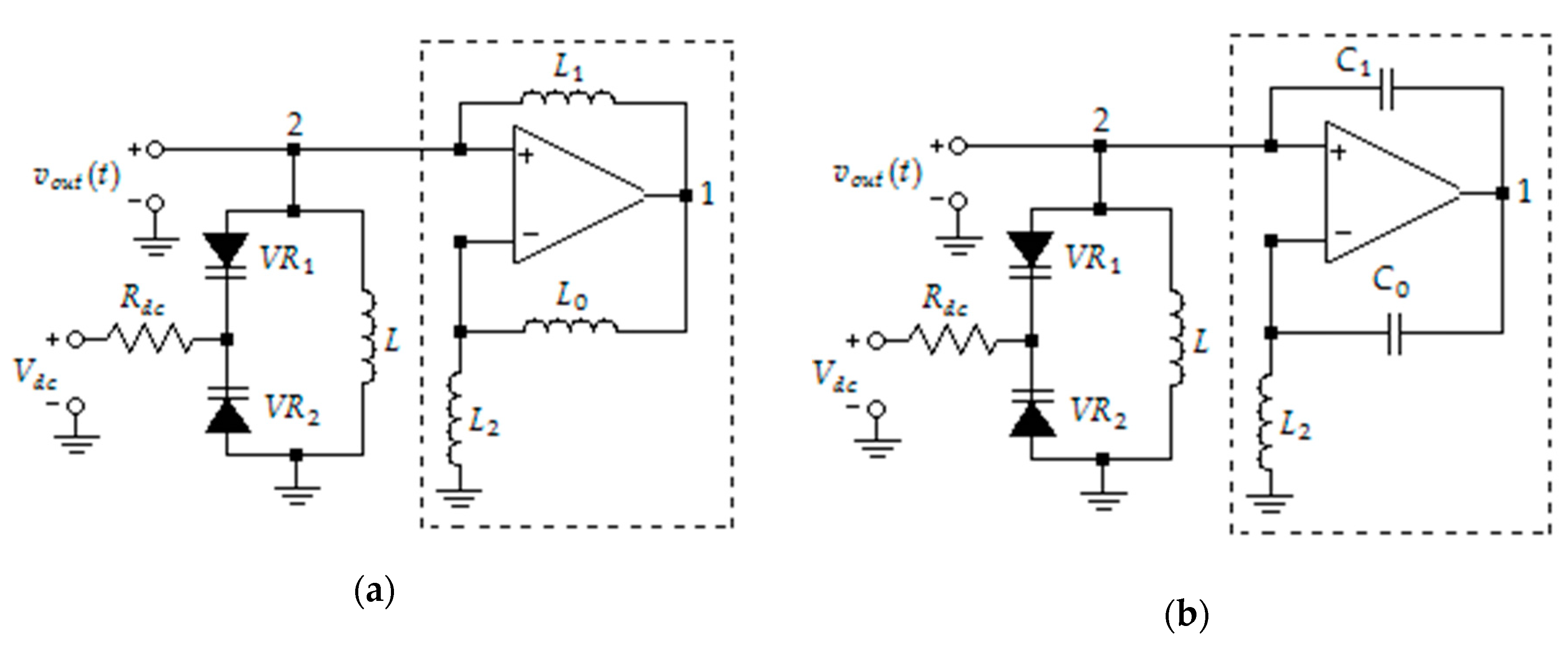
2. Architecture of Oscillators

Figure 1 shows the general VCO electronic diagram. The circuit inside the dashed rectangular is the negative impedance converter. The input impedance observed at the noninverting terminal of the OPA is as follows [16]:
Z i n = Z 2 Z 1 Z 0
where Zin is the input impedance seen by the noninverting terminal of the OPA, Z0 is the impedance between the inverting input and output of the OPA, Z1 is the impedance between the noninverting input and output of the OPA, and Z2 is the impedance between the inverting terminal of the OPA and ground. The step-by-step derivation of Equation (1) is given in [18] (pp. 349–350).
In Reference [15,16,17], one of the impedances Z0, Z1, or Z2 is capacitive, and the other two are resistive.
The presence of significant resistances in the circuit of any oscillator leads to an increase in thermal noise [19]; therefore, in this study, the impedances Z0, Z1, and Z2 are capacitive or inductive.
In the circuit of Figure 1, inductor L and two contrary connected varactors VR1 and VR2 present the tank circuit of the VCO. Resistor Rdc isolates the dc control voltage line from the VCO tank.
As can be seen in Figure 1, the tank circuit is connected to the noninverting input of the OPA rather than its output. This feature of the proposed VCO allows extending operation frequency range beyond the unity-gain bandwidth of OPA.
Figure 2 shows VCO circuits based on impedance converters with two inductors and one capacitor. The circuits in Figure 2a,b introduce positive feedback through inductor L1 and capacitor C1, respectively.
Figure 3 presents VCO circuits on the base of impedance converters with three inductors (a) and two capacitors and one inductor (b).
The oscillator circuits based on impedance converters in which a capacitor is used between the inverting input of the OPA and ground are not considered.
Further, in the article, we will analyze in detail the VCO circuit presented in Figure 2a, and where necessary, we will refer to other VCO configurations.

3. Converter Analysis
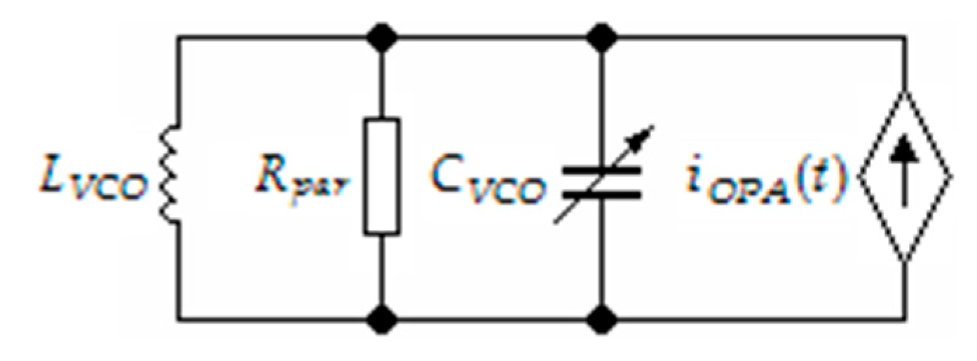
Before analyzing the VCO circuit of Figure 2a, let’s examine the operation of the converter at frequencies exceeding the OPA bandwidth. Figure 4a shows the test circuit. We assume that the OPA unity-gain bandwidth is 900 MHz, the slew rate is 1600 V/μs, the open-loop gain is 1000 V/V, and the test signal is a sinusoidal voltage with a frequency of 1 GHz and peak amplitude of 2 V.
Figure 4b shows the voltage waveforms at the noninverting input (curve 2) and the output of the OPA (curve 1). As we can see in Figure 4b, the slew rate of the OPA is not sufficient to ensure the shape of the OPA output voltage as that at the noninverting input. Therefore, we observe a triangular voltage waveform at the OPA output (node 1). Moreover, Figure 4b shows that the OPA output voltage lags the input voltage by 90°. From a comparison of the circuits in Figure 2a and Figure 4a, we can see that instead of the test generator in Figure 4a, a parallel resonant circuit is used in Figure 2a. We will show further that the shape of the voltage curves in the circuit of Figure 2a will be the same as in Figure 4b; however, curve 2 will correspond to the voltage at the output of the VCO.

4. VCO Analysis

The electronic part of the VCO introduces an alternating current (ac) source iOPA(t) into the tank circuit, as shown in Figure 5, where CVCO and LVCO are, respectively, the VCO total capacitance and inductance, and Rpar is the equivalent parallel resistance of the tank circuit at the fundamental frequency. Essentially the current iOPA (t) is the feedback current flowing through inductor L1.
The VCO total capacitance includes the capacitance of the contrary connected varactors VR1 and VR2, the input capacitance of the OPA, and the parasitic capacitance of the printed circuit board (PCB). Therefore,
C V C O ( V d c ) = C V R 1 ( V d c ) C V R 2 ( V d c ) C V R 1 ( V d c ) + C V R 2 ( V d c ) + C P C B + C O P A
As we can see in Equation (2), the VCO capacitance is a function of voltage Vdc because the varactor capacitance depends on this voltage. Onwards, inductor L1 provides positive shunt–shunt feedback.
By applying the y-parameter analysis to the positive feedback network, we find that y11 parameter incorporates into the tank circuit. Since y11 = 1/funL1, inductance L1 appears in parallel with tank inductance L, where ωfun is the fundamental angular frequency of oscillation.
Therefore, the total VCO tank circuit inductance is given by
L V C O = L 1 L
The current iOPA(t) flows through the tank circuit. However, only the first harmonic of the current flow creates a significant voltage drop across the tank. The second, third, and subsequent current harmonics create insignificant voltage drops that can be neglected.
We should also note that the tank circuit is connected to the noninverting input of the OPA, where the input impedance is extremely high. Therefore, the OPA does not practically short-out the tank circuit.
This property of the proposed VCO allows obtaining high voltage amplitude of the generated voltage vout(t), which is not limited by the OPA output. Indeed, we can describe the VCO output voltage by the following equation:
v o u t ( t ) = | I O P A , 1 ( V d c ) | R p a r ( V d c ) sin [ ω f u n ( V d c ) t + φ 1 ( V d c ) ]
where |IOPA,1(Vdc)|, ωfun(Vdc), and φ1(Vdc) are, respectively, the amplitude, frequency and initial phase of the first harmonic of current iOPA(t). Therefore, we can see from (4) that the amplitude of the generated sinusoidal voltage is proportional to |IOPA,1| and Rpar. In a virtual case of lossless tank circuit, i.e., when Rpar → ∞, the amplitude of the output voltage would tend to infinity.
This is a unique property of the proposed OPA oscillator because, for the Colpitts and Hartley OPA oscillators [8], the output amplitude satisfies the following inequality:
V m 4 V s a t R p a r π ( R C + R p a r )
where Vsat is the OPA saturation voltage, and RC is the resistance of the load resistor connected between the OPA output and tank circuit.
Since the OPA saturation voltage in (5) is less than the power supply voltage Vcc, the oscillation amplitude is also less. Figure 6a illustrates the behavior of the OPA output voltage (curve 1) and the oscillator output voltage (curve 2) for the Colpitts oscillator operating at frequency of 53 MHz with Vcc = ±5 V and voltage peak amplitude of 3.7 V. We can also observe in Figure 6a that the shape of the voltage at the output of the OPA, in this particular case, is trapezoidal, which means the slew rate of the OPA is not high enough to ensure a rectangular shape.
With a further increase in the frequency of the generated oscillations in the Colpitts oscillator, the voltage shape at the output of the OPA becomes triangular with the amplitude less than Vsat. In this case, also, the amplitude of sinusoidal oscillations in the Colpitts oscillator will always be less than the magnitude of triangular oscillations.
A completely different relationship exists between the amplitudes of the voltages at the output of the OPA (node 1) and the oscillator (node 2) in the circuit in Figure 2a. Figure 6b illustrates the behavior of the OPA output voltage (curve 1) at node 1 and the oscillator output voltage (curve 2) at node 2 for the proposed oscillator operating at frequency of 667 MHz with the same OPA, power supply voltages and output peak amplitude of 4 V. As can be seen in Figure 6b, the amplitude of the sinusoidal voltage can be much larger than the voltage amplitude at the output of the OPA (node 1).
Therefore, the proposed VCO can operate at frequencies significantly exceeding the unity-gain bandwidth of OPA.
It should also be noted that by choosing a low-noise OPA, the phase noise of the VCO will be determined mainly by the noise of the tank circuit.

5. Amplitude of Oscillations

Let us determine the amplitude of the sinusoidal voltage at the output of the VCO (node 2). Assume the voltage at node 1 be triangular, as shown in Figure 6b (curve 1). For the triangle wave, we can describe the voltage at node 1 by the complex exponential Fourier series as follows:
v O P A ( t ) = 0.5 μ = V μ e j μ ω f u n t
where Vμ is the complex amplitude of the harmonic number μ of voltage vOPA(t).
The complex amplitude Vμ can be represented as
V μ = | V μ | e j θ μ
where |Vμ| and θμ are the amplitude and phase of the voltage harmonic number μ, respectively.
As is well known [20], the amplitude of the voltage harmonic μ for the triangle wave is
| V μ | = 8 V t r i a n g l e π 2 μ 2 sin μ π 2
where Vtriangle is the amplitude of the triangular voltage at the OPA output.
The feedback current iOPA(t), which flows from node 1 into the tank circuit, we also present by the complex exponential Fourier series
i O P A ( t ) = 0.5 μ = I O P A , μ e j μ ω f u n t
where IOPA,μ is the complex amplitude of the current harmonic number μ.
The complex amplitude IOPA,μ we write in polar form as follows:
I O P A , μ = | I O P A , μ | e j φ μ
where |IOPA,μ| and φμ are the amplitude and phase of the current harmonic number μ, respectively.
In the ac equivalent circuit of the VCO shown in Figure 5, the feedback inductor L1 is in parallel with tank inductor L. The feedback current iOPA(t) flows through inductor L1 and tank circuit due to the applied voltage vOPA(t). Considering the forward transfer admittance of the feedback network y12 = −1/funL1 and parallel connection of inductors L1 and L in the equivalent circuit of Figure 5, by Ohm’s law, we have
I O P A , μ = V μ / ( j ω f u n L 1 L ) = j V μ / ( ω f u n L 1 L )
By substitution of (7) and (8) into (11), we get
I O P A , μ = 8 V t r i a n g l e ω f u n L 1 L π 2 μ 2 sin μ π 2 exp [ j ( θ μ + π 2 ) ]
The first harmonic of current iOPA(t) is of interest because for the higher harmonics, the equivalent resistance of the tank circuit is negligible, and they do not create a significant voltage drop. By substitution μ = 1 into (12) gives
I O P A , 1 = 8 V t r i a n g l e ω f u n L 1 L π 2 exp [ j ( θ 1 + π 2 ) ]
We determine the first harmonic of the voltage across the tank by multiplying the complex amplitude IOPA,1 and the equivalent resistance of the tank at resonance Rpar as follows:
V o u t , 1 = 8 V t r i a n g l e R p a r ω f u n L 1 L π 2 exp [ j ( θ 1 + π 2 ) ]
By comparing (7) when μ = 1 and (14), we can state that the first harmonic of voltage across the tank leads the first harmonic of triangular voltage at the OPA output by 90°, which is confirmed by Figure 6b.
From (14) it follows that the amplitude of the voltage across the tank is
| V o u t , 1 | = 8 V t r i a n g l e R p a r ω f u n L 1 L π 2
Analyzing (15), we can observe that the amplitude of the VCO output voltage |Vout,1| is directly proportional to resistance Rpar and inversely proportional to inductance L1L. As already indicated in the analysis of Equation (4), when using a tank circuit with low losses, the voltage amplitude at the output of the VCO can be significant.
Let us simplify (15) by considering the case when L1 ˃˃ L. In this case, L1LL and we can write Equation (15) in the following form:
| V o u t , 1 | = 8 V t r i a n g l e R p a r ω f u n L π 2
At resonance we have
ω f u n L = L C V C O = ρ
where ρ is the tank circuit characteristic impedance.
As is well known [21] (p. 909), the equivalent resistance of the parallel tank at resonance is
R p a r = ρ 2 r s
where rs is the series loss resistance of the tank circuit.
Substituting (17) and (18) into (16) gives
| V o u t , 1 | = 8 V t r i a n g l e ρ r s π 2
Since the ratio of ρ to rs in (19) is equal to the quality factor of the parallel tank circuit (Q), then we write (19) in the following form:
| V o u t , 1 | = 8 V t r i a n g l e Q π 2
We derived Equation (20) under the condition of an ideal OPA with infinite input resistance, which does not load the tank circuit. However, in the real OPA, the input resistance is not infinite; therefore, in (20), we should use the loaded quality factor. Therefore,
| V o u t , 1 | = 8 V t r i a n g l e Q L π 2
where QL is the quality factor of the loaded VCO tank circuit.
For the VCO shown in Figure 2b, following the same analysis as for the circuit of Figure 2a, we obtain that the amplitude of oscillations is
| V o u t , 1 | = 8 V t r i a n g l e ω f C V C O C 1 R p a r π 2 = 8 V t r i a n g l e ω f ( C V C O + C 1 ) R p a r π 2
From the analysis of Equation (22), it follows that the capacitance of the positive feedback capacitor C1 should be much less than the capacitance CVCO; in this case, the capacitance C1 will not affect the frequency of generated oscillations.
Given that at the resonant frequency
ω f ( C V C O + C 1 ) = 1 ρ
We transform Equation (22) as follows:
| V o u t , 1 | = 8 V t r i a n g l e R p a r π 2 ρ
Considering that Rpar/ρ = Q in (24), we obtain again Equation (20), which transforms to (21) due to the loaded tank circuit.
The amplitude of the generated sinusoidal voltages in the VCO circuits in Figure 3a,b is also calculated by Equation (21).

6. VCO Start-Up Conditions

According to the Barkhausen criteria [22], to provide the sustained oscillations, the following conditions must have a place:
| A | | β | = 1
φ A + φ β = 0
where |A| and |, and φA and φβ are, respectively, the gains and initial phases of impedance converter and feedback network.
As shown in Figure 4b, the voltage gain of the impedance converter is less than unity. We determine the feedback network ratio as follows:
| β | = | V o u t , 1 | | V 1 |
where |V1| is the voltage amplitude of the first harmonic of triangular voltage at the output of the OPA (node 1).
Substituting (8) at μ = 1 and (21) into (27) gives
| β | = Q L
We can conclude from (25) and (28) that at the steady-state the gain of the impedance converter is
| A | = 1 | β | = 1 Q L
To start the oscillations, the product of |A| and |β| is made higher than unity, and when the amplitude reaches a constant value |Vout,1|, this product becomes equal to unity.
From relations (28) and (29), it follows that in the proposed oscillators, the feedback network coefficient |β| is more than unity, and the gain of the active network |A| is less than unity; this is a unique property because in the Colpitts and Hartley oscillators the opposite is true, i.e., |A| ˃ 1 and |β| < 1. Due to this property, the proposed VCO can operate at frequencies significantly exceeding the unity-gain bandwidth of an OPA with sufficiently large oscillation amplitudes.

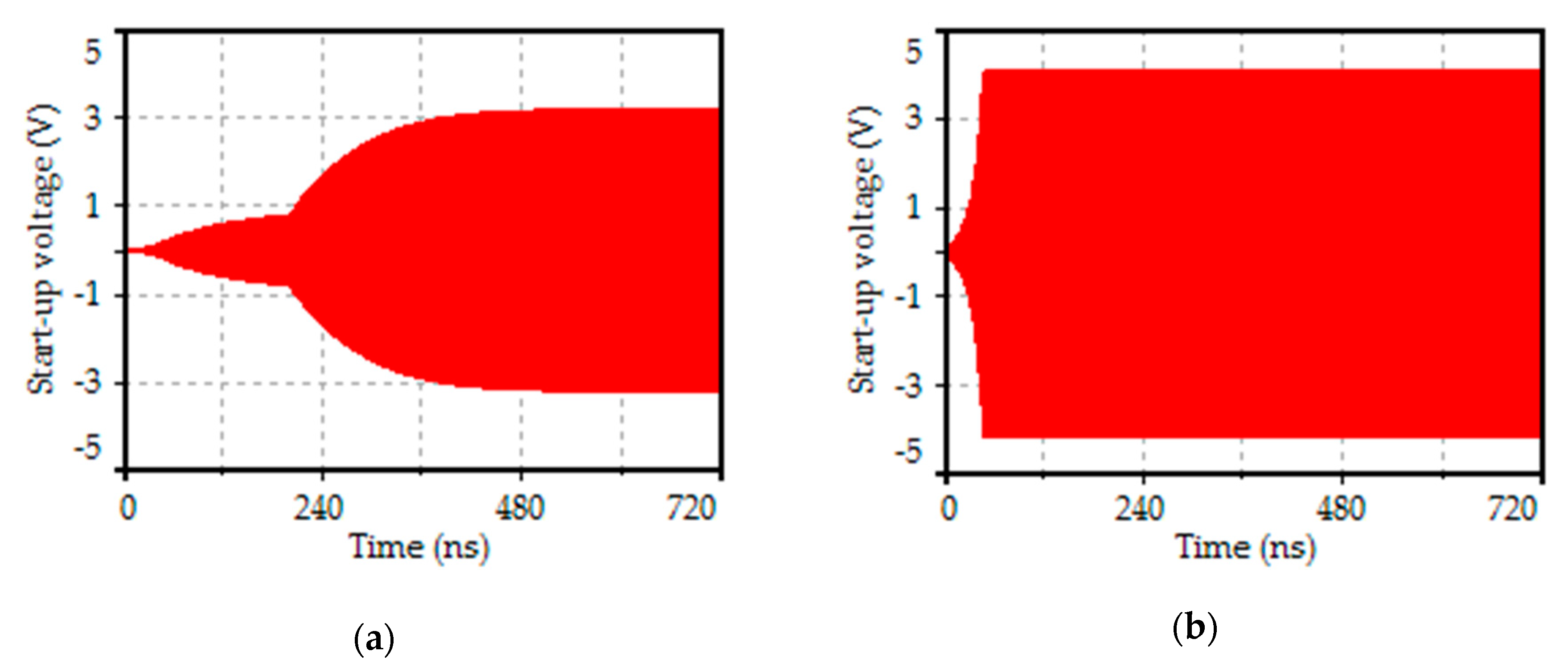
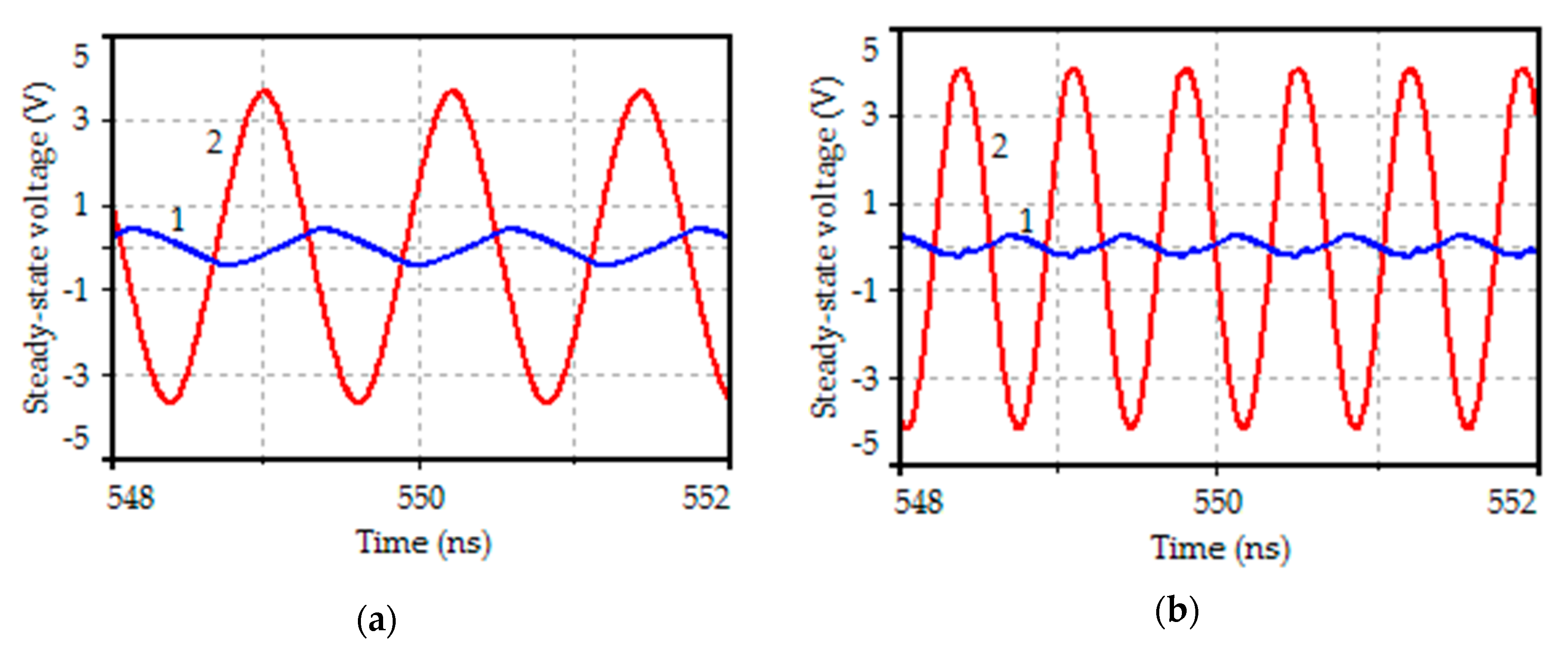
7. Simulation and Discussion

The circuit of Figure 2a was simulated with the help of Multisim (ed. 14.1) using SPICE models of a real OPA, varactors, and RF coil to confirm the operation efficiency of the proposed VCO topology. We selected ultra-low noise, high-speed OPA LMH6629MF with −3 dB bandwidth of 900 MHz, slew rate of 1600 V/μs, input voltage noise of 0.69 nV/√Hz, and power supply voltage ±5 V. We also selected UHF varactors BB215 and a 3.3 nH RF coil. The other component values are as follows: L1 = L2 = 1 μH, C = 100 nF, and Rdc = 1 kΩ.
Figure 7 shows the simulated VCO schematic with chosen component values.
Figure 8 shows the VCO start-up voltage in the interval 0–720 ns at Vdc = 1 V (a) and Vdc = 11 V (b). As we can see in Figure 8, the oscillations reach the steady-state condition within 500 ns at Vdc = 1 V and 50 ns at Vdc = 11 V. Thus, the starting time of VCO is speedy.
Figure 9 shows the steady-state voltage waveforms at nodes 1 and 2 when Vdc = 1 V (a) and Vdc = 11 V (b). As can be seen in Figure 9, the amplitude of the triangular voltage at the output of OPA (node 1) is much less than the amplitude of the sinusoidal voltage at the VCO output (node 2).
From the simulation results shown in Figure 9, it is observed that the THD is 1.5% at Vdc = 1 V and 1.7% at Vdc = 11 V, which corresponds to −36.5 dB and −35.4 dB, respectively.
Since in the microwave frequency range, the THD value of −30 dB is considered quite well [23] (p. 291), [24], we can argue that the designed VCO is a low-distortion oscillator.
Let us check Equation (21). From Figure 9a it can be observed that Vtriangle = 0.37 V and |Vout,1| = 3.19 V. To find the loaded quality factor QL, we use the property of the parallel tank circuit that the current circulating in the tank circuit Itank in QL times higher than the current in the general circuit Ires [21] (p. 911).
Figure 10a illustrates the location of currents Itank and Ires in the VCO tank circuit.
Therefore, the loaded quality factor can be calculated by the following equation:
Q L = I t a n k / I r e s
By simulation, we find that Itank = 127 mA and Ires = 15 mA. Substituting the currents into (30) gives that QL = 8.5. Further, by substitution of Vtriangle and QL into Equation (21), we calculate that |Vout,1| = 2.76 V. So, the relative error of amplitude calculation by Equation (21) is only 13.5%.
Figure 10b shows the VCO tuning characteristics. As we can see in Figure 10b, the VCO operates from 830 MHz to 1.429 GHz, i.e., the tunable band is 599 MHz. Thus, the designed circuit is a wideband VCO, which operates in the frequency range, significantly exceeding the bandwidth of the OPA. Indeed, the bandwidth of the LMH6629MF is 900 MHz, but the highest VCO frequency is 1.429 GHz. Using the equation for maximum signal frequency [12], we can find that with the OPA LMH6629MF in the Colpitts or Hartley VCO, the 4 V amplitude of the sinusoidal voltage corresponds to a frequency that is less than 64 MHz.
Thus, by using the proposed VCO topology, we can increase the maximum operating frequency by more than 22 times. Figure 11 shows the simulated power spectrum of the designed VCO at the lowest frequency (a) and the highest frequency (b). As we can see in Figure 11a, only the second and third harmonics contribute to the THD because the fourth and subsequent harmonics attenuated for at least 90 dB compared to the first harmonic. By analyzing Figure 11b, we find that the second and upper harmonics decrease slowly. However, the second and other harmonics attenuated by at least 36 dB.
One of the essential characteristics of an oscillator operating at microwave frequencies is phase noise. To calculate the phase noise of the simulated VCO, we use the improved Leeson’s formula [25] (p. 128)
P N ( f m ) = 10 log { F k T 2 P o u t [ f f u n 2 f c f m 3 4 Q L 2 + ( f f u n 2 Q L f m ) 2 + ( 1 + f c f m ) ] }
where PN is the phase noise (dBc/Hz), F is the noise figure of the oscillator active device (dB), k 1.38 × 10 23 is the Boltzmann constant (J/K), T is the temperature in Kelvin, Pout is the oscillator output power, ffun is the frequency of oscillations (Hz), fc is the 1/f corner frequency of active device (Hz), and fm is the offset frequency (Hz).
According to Reference [7], the noise figure of OPA LMH6629MF is 8 dB. Figure 11a,b shows that Pout = 9 dBm when Vdc = 1 V and Pout = 11 dBm when Vdc = 11 V. Figure 10b indicates that the minimum frequency of oscillations is 830 MHz, and the maximum is 1429 MHz. From Reference [7] (p.15, Figure 28) we find that fc = 4 kHz. The loaded quality factor, QL, is 8.5 and 2.6 for Vdc = 1 V and 11 V, respectively.
Figure 12 shows the dependence of the phase noise versus offset frequency for the VCO shown in Figure 7. As can be seen in Figure 12, the VCO phase noise changes from −153.4 dBc/Hz to −139.3 dBc/Hz at 100 kHz offset frequency when the control voltage varies from 1 V to 11 V. Thus, the maximum in-band phase noise is −139.3 dBc/Hz at fm = 100 kHz.
Let us compare the characteristics of the simulated VCO with the best VCO designs operating in the microwave frequency range. The commonly used FoM includes phase noise (PN), the ratio of ffun to fm, and the power consumption (Pc) [26].
F o M ( f m ) = P N ( f m ) d B c 20 log ( f f u n / f m ) + 10 log ( P c / 1 mW )
In Equation (32), the second term allows one to compare the phase noise of the oscillators determined at different frequencies and various frequency offsets. The third term in (32) has a positive sign if Pc ˃ 1 mW and negative if Pc < 1 mW. Thus, the smaller the value of FoM, the higher efficiency of the oscillator.
Table 1 shows a comparison of the designed VCO with microwave oscillators that have been reported in journals and conference proceedings.
We can see in Table 1 that the designed VCO has the best FoM among oscillators fabricated in GaN HEMT, SiGe, HEMT, GaAs pHEMT, and SiGe BJT technologies where, in general, power consumption is high enough. Moreover, as shown in Table 1, the designed VCO can even compete with the latest achievements in CMOS VCOs; this is due to low phase noise and in spite of higher power dissipation.

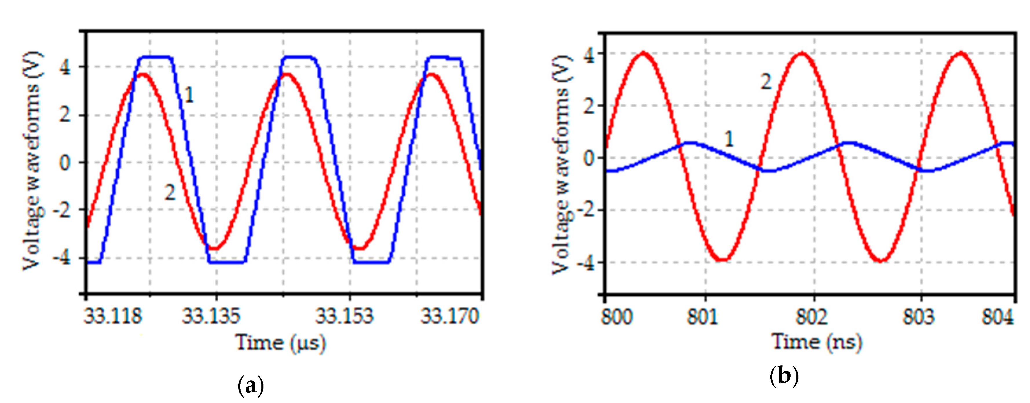
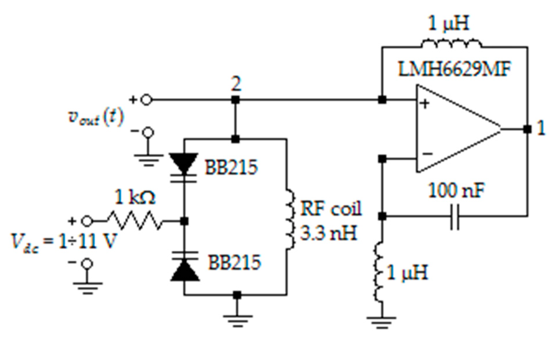
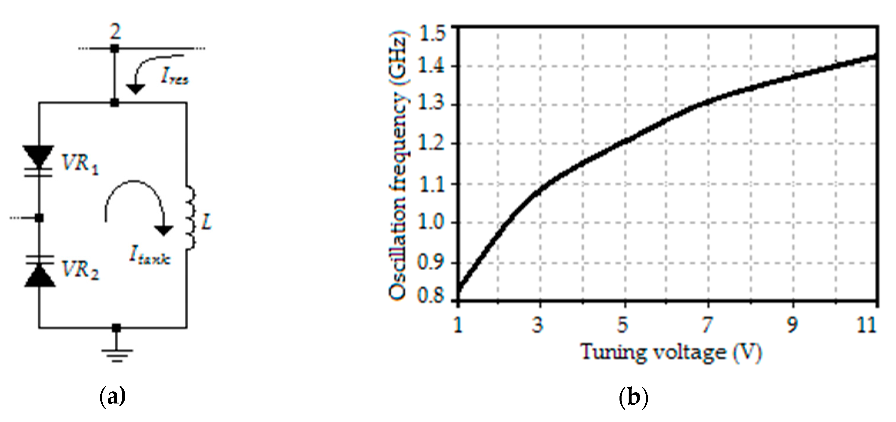
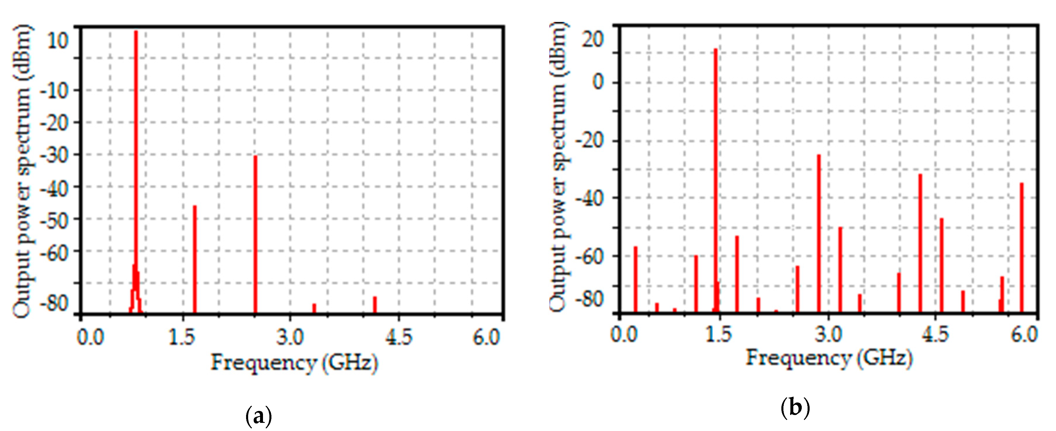
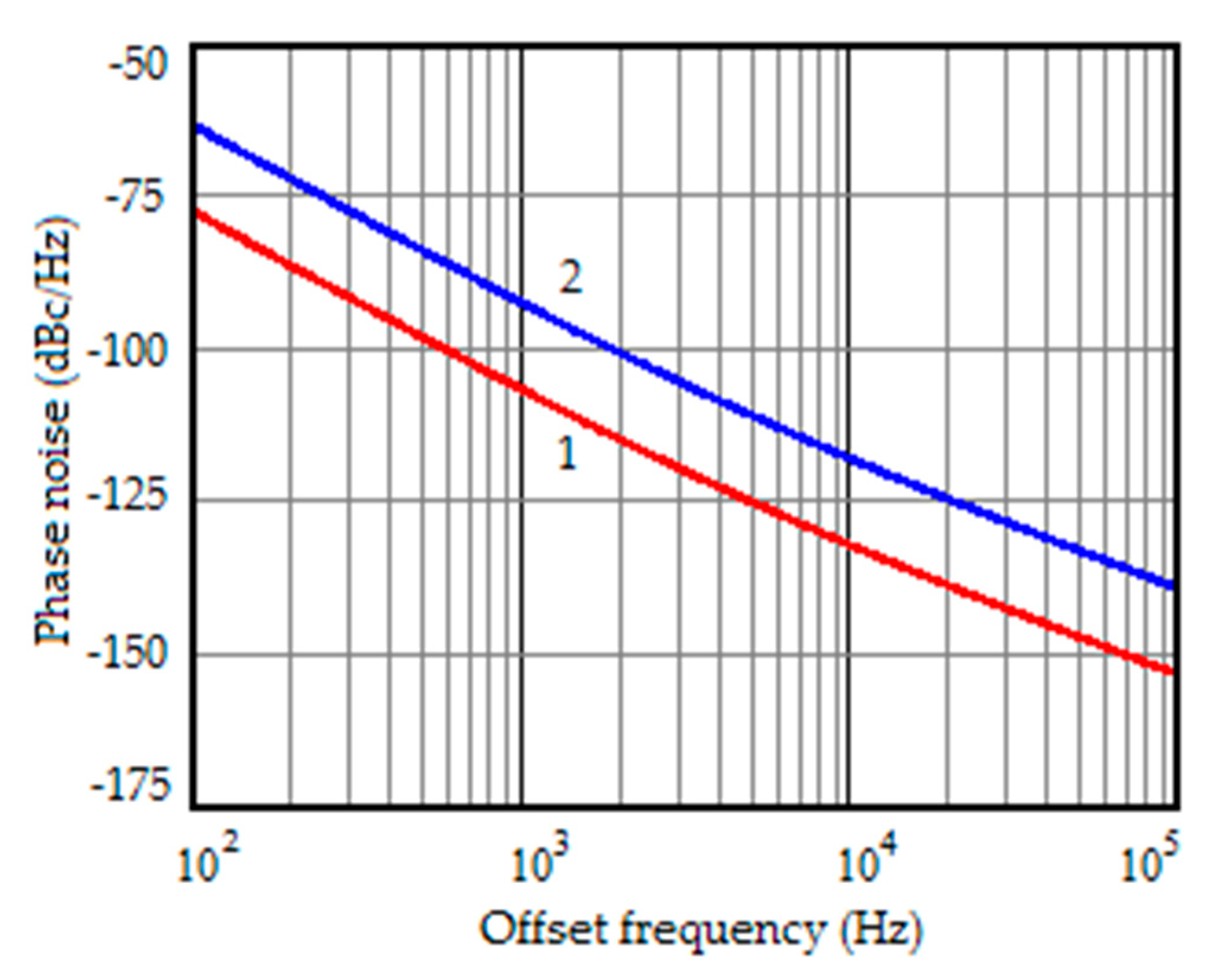
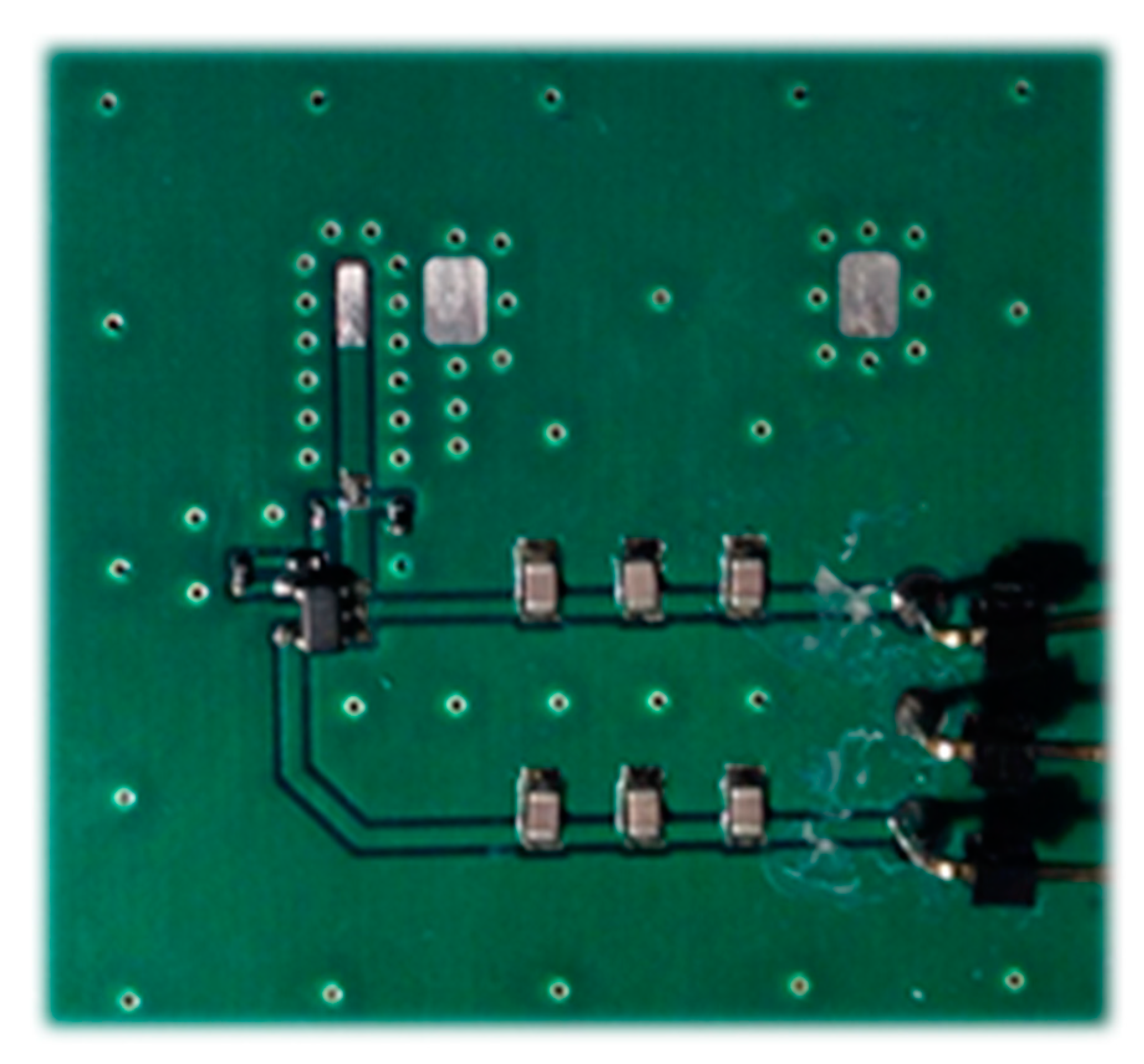
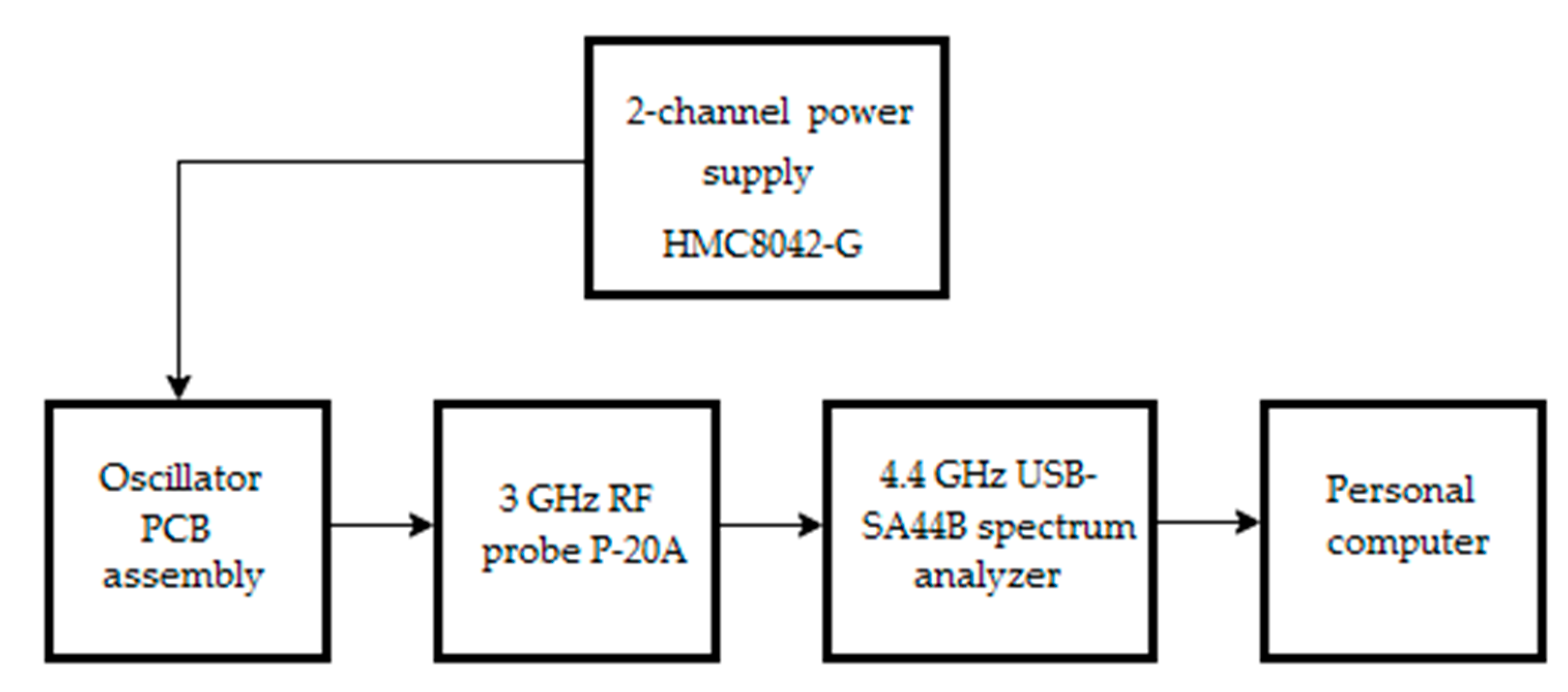
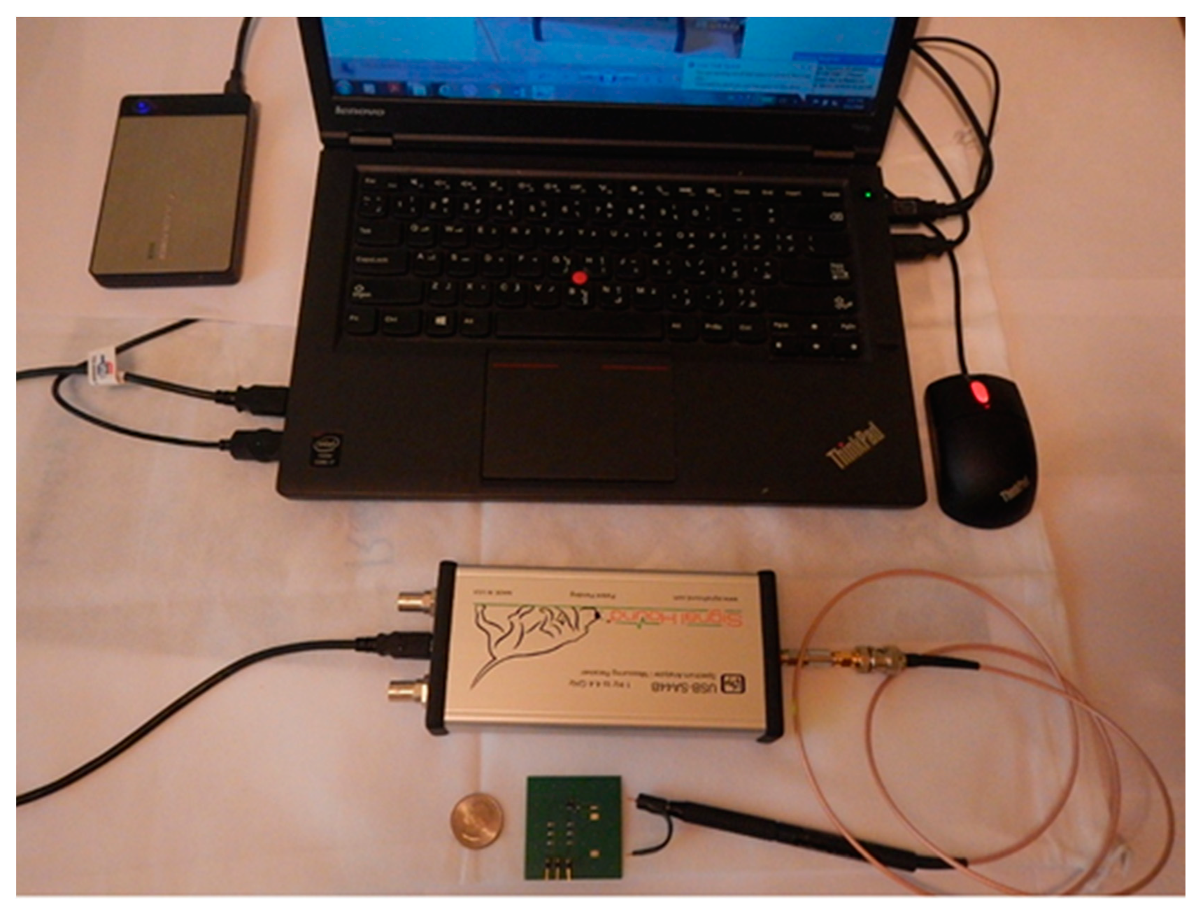
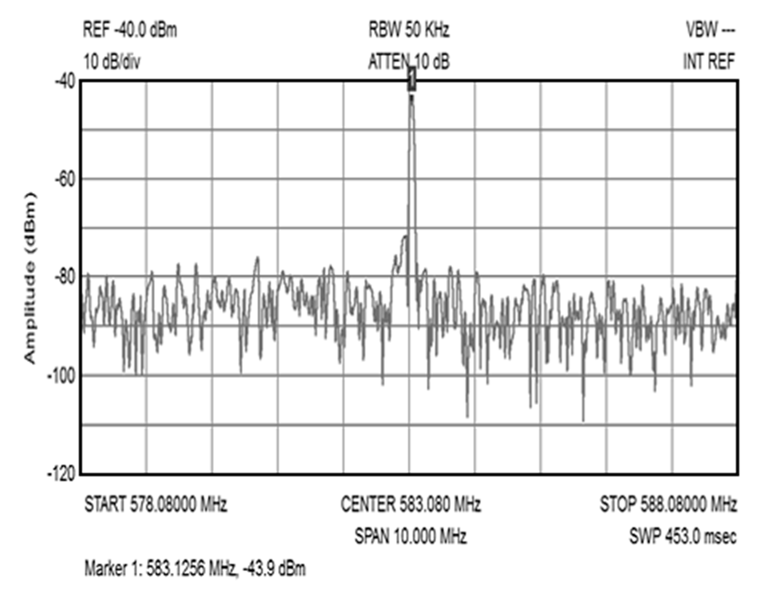
8. Experimental Results

We fabricated a prototype of oscillator circuit shown in Figure 2b. Figure 13 shows a PCB assembly of the oscillator. We selected OPA LMH6624 (Texas Instruments) with a slew rate of 350 V/μs, gain bandwidth of 1.5 GHz, supply voltage ±5 V, and the following passive components: L0 = 200 nH (2 × ELJRFR10), L = 8.2 nH (high-quality coil ELJQF8N2), and C1 = 2.2 pF (ceramic capacitor C0603C0G1E2R2C030BA). We removed varactors VR1 and VR2, and inductor L2 from the oscillator circuit for simplicity, i.e., CVR1 = CVR2 = 0, and L2 = ∞.
A spectrum analyzer USB-SA44B (Keysight Technologies) was used to measure the output power spectrum. We used RF probes P-20A (Auburn Technology) to connect the oscillator output through a capacitive divider to the spectrum analyzer. Figure 14 shows the block diagram of the measurement experiment.
Figure 15 shows the connection between the core elements of the measurement block diagram. The 2-channel power supply HMC8042-G (Rohde and Schwarz) is not shown in Figure 15.
Figure 16 shows the measured power spectrum. As we can see in Figure 16, the frequency of oscillations is 583.1 MHz. The measured power is −43.9 dBm. However, in estimating the real output power, we should consider 21 dB probes attenuation, 10 dB “Attenuation” setting in the spectrum analyzer, and 13 dB insertion loss of the capacitive divider. Thus, the actual power at the output of the fabricated oscillator was around 0 dBm.

9. Conclusions

This article has proposed a new type of VCO based on resistorless negative impedance converter circuits. A distinctive feature of each proposed VCO circuit is that its output is located at the noninverting input of the OPA; this allows us to significantly increase the frequency and amplitude of the generated oscillations. Mathematical modeling of the amplitude of the oscillations and the start-up conditions were carried out. We have shown that, unlike existing oscillators of the Colpitts and Hartley topology, in the proposed VCO, the gain is less than unity, and the feedback coefficient is greater than unity. Therefore, the proposed oscillators can operate at frequencies exceeding the unity-gain bandwidth. The advantage of the proposed VCO circuit is also the fact that the amplitude of the generated sinusoidal oscillations can be dozens of times higher than the magnitude of the nonsinusoidal oscillations at the output of the OPA. The designed and simulated VCO uses ±5 V supply voltage and operates in a wide frequency range from 830 MHz to 1429 MHz showing a maximum in-band THD of 1.7% while the OPA bandwidth is only 900 MHz; the amplitude of oscillations varies from 3.2 V to 4 V. It has a maximum in-band phase noise of −139.3 dBc/Hz at 100 kHz offset frequency and has an outstanding value of FoM of −198.6 dBc/Hz. The conducted comparison of the designed VCO with VCOs in previously published studies concerning standard FoM has shown that the proposed oscillator is about 8–15 dB more efficient than the GaN HEMT, GaN pHEMT, HEMT, and SiGe VCOs and close to the best CMOS VCOs. We have shown that for the same OPA, the operating frequency of the proposed VCO is 22 times higher than that of the Colpitts and Hartley oscillators. The fabricated prototype-oscillator based on OPA LMH6624 operates at a frequency of 583.1 MHz with a power level of 0 dBm.
The proposed OPA VCO circuits are easy to design. They do not require settings during the manufacturing process. These oscillators can be used from high-frequency to the microwave frequency range. Since the power consumption in the proposed VCO is higher than in the CMOS oscillators, the field of application extends to communications, navigation, and radar equipment with an uninterruptible power supply line. As the proposed schemes do not require tuning, they can be useful in conducting laboratory works in the departments of electronics at universities.
Our future work will include mathematical modeling of phase noise in the proposed oscillators using the method of impulse sensitivity functions.

Author Contributions

This article presents the collective work of two authors. The authors (A.R. and V.U.) jointly participated in the conceptualization of the problem, development of oscillator circuits and mathematical modeling, numerical calculations, and writing the article. V.U. participated in prototype oscillator design and fabrication. A.R. conducted project administration. All authors have read and agreed to the published version of the manuscript.

Funding

This research received no external funding.

Acknowledgments

The authors express thanks to engineer A. Kolesnik for technical support.

Conflicts of Interest

The authors declare no conflict of interest.

Nomenclature

ZinInput impedance seen by the noninverting terminal of OPA
Z0Impedance between the inverting input and output of OPA
Z1Impedance between the noninverting input and output of OPA
Z2Impedance between the inverting input of OPA and ground
LInductor of the tank circuit
VR1 and VR2Varactors of the tank circuit
RdcResistor isolating the dc control voltage line from the VCO tank
L1Positive feedback inductor
C1Positive feedback capacitor
L0Negative feedback inductor
C0Negative feedback capacitor
L2Inductor between inverting terminal of OPA and ground
CVCOVCO total capacitance
LVCOVCO total inductance
COPAInput capacitance of OPA
CPCBParasitic capacitance of PCB
CVR1Capacitance of varactor VR1
CVR2Capacitance of varactor VR2
y11Input admittance of feedback network
iOPA(t)Feedback current flowing through impedance Z1
vout(t)Output voltage of VCO
IOPA,1Complex amplitude of the first harmonic of current iOPA(t)
ωfunAngular frequency of the first (fundamental) harmonic of current iOPA(t)
φ1Phase of the first harmonic of current iOPA(t)
RparEquivalent parallel resistance of the tank circuit at the fundamental frequency
VsatSaturation voltage of OPA
RCLoad resistor connected between OPA output and tank circuit in the Colpitts and Hartley oscillators
vOPA(t)Voltage at the output of OPA (node 1)
VμComplex amplitude of harmonic number μ of voltage vOPA(t)
|Vμ|Amplitude of harmonic number μ of voltage vOPA(t)
θμPhase of harmonic number μ of voltage vOPA(t)
VtriangleAmplitude of triangular voltage at OPA output
IOPA,μComplex amplitude of current harmonic number μ
|IOPA,μ|Amplitude of current harmonic number μ
φμPhase of current harmonic number μ
ρTank circuit characteristic impedance
rsSeries loss resistance of the tank circuit
QQuality factor of the parallel tank circuit
QLQuality factor of the loaded parallel tank circuit
|A|Gain of impedance converter
|β|Gain of feedback network
φAInitial phase of impedance converter
φβInitial phase of feedback network
|V1|Voltage amplitude of the first harmonic of triangular voltage at the output of OPA (node 1)
ItankCurrent circulating in the tank circuit at resonance
IresExternal current entering the tank circuit at resonance
FoMFigure of merit
PcPower consumption of oscillator
PNPhase noise
PoutOscillator output power
FNoise figure
kBoltzmann constant
TTemperature in Kelvin
fc1/f corner frequency
fmOffset frequency
ffunFrequency of oscillations in Hz

Abbreviations

The following abbreviations exist in the manuscript:
ACAlternating current
BJTBipolar junction transistor
CMOSComplementary metal-oxide-semiconductor
FoMFigure of merit
GaAsGallium arsenide
GaNGallium nitride
HBTHeterojunction bipolar transistor
HEMTHigh-electron-mobility transistor
OPAOperational amplifier
PCBPrinted circuit board
pHEMTPseudomorphic high-electron-mobility transistor
RFRadio frequency
SiGeSilicon germanium
SPICESimulation program with integrated circuit emphasis
THDTotal harmonic distortion
VCOVoltage controlled oscillator

References

  1. Schulz:, M.; Strobel, A.; Ellinger, F. System considerations and VCO design for a local positioning system at 2.4 GHz for rescue of people on ships and in sea. In Proceedings of the IEEE 10th Workshop on Positioning, Navigation and Communication (WPNC), Dresden, Germany, 20–21 March 2013. [Google Scholar] [CrossRef]
  2. Carlowitz, C.; Esswein, A.; Weigel, R.; Vossiek, M. A low power pulse frequency modulated UWB radar transmitter concept based on switched injection-locked harmonic sampling. In Proceedings of the 7th German Microwave Conference, Ilmenau, Germany, 12–14 March 2012. [Google Scholar]
  3. Scherbina, K.A.; Pechenin, V.V.; Vonsovitch, M.A. Phase-locked loop combined system of voltage controlled oscillator. In Proceedings of the IEEE 9th International Kharkiv Symposium on Physics and Engineering of Microwaves, Millimeter and Submillimeter Waves (MSMW), Kharkiv, Ukraine, 20–24 June 2016. [Google Scholar] [CrossRef]
  4. Grebennikov, A. RF and Microwave Transistor Oscillator Design; John Wiley & Sons, Ltd.: Chichester, UK, 2007. [Google Scholar] [CrossRef]
  5. Gonzalez, G. Foundations of Oscillator Circuit Design; Artech House: Boston, MA, USA, 2007. [Google Scholar]
  6. Everard, J. Fundamentals of RF Circuit Design: With Low Noise Oscillators; John Wiley& Sons, Ltd.: Chichester, UK, 2001. [Google Scholar] [CrossRef]
  7. LMH6629 Ultra-Low Noise, High-Speed Operational Amplifier with Shutdown Datasheet (Rev. I). Available online: http://www.ti.com/lit/ds/symlink/lmh6629.pdf (accessed on 1 December 2014).
  8. Ulansky, V.; Machalin, I.; Tkalich, O. Analysis and design of voltage-controlled oscillators using high-speed operational amplifiers. Proc. Natl. Aviat. Univ. 2002, 3, 171–178. [Google Scholar] [CrossRef]
  9. Ulansky, V.V.; Kolesnik, A.A.; Elsherif, H.M. A new high-performance OPA based VCO for microwave applications. In Proceedings of the 2014 IEEE Microwaves, Radar and Remote Sensing Symposium, Kiev, Ukraine, 23–25 September 2014. [Google Scholar] [CrossRef]
  10. Rashid, M.H. Microelectronic Circuits. Analysis and Design; Cengage Learning: Stamford, CT, USA, 2011; p. 883. [Google Scholar]
  11. Jacas, M.M.; Llopis, F. LC sine-wave oscillators using general-purpose voltage operational-amplifiers. Int. J. Electr. Eng. Educ. 2007, 44, 244–248. [Google Scholar] [CrossRef] [Green Version]
  12. Boylestad, R.; Nashelsky, L. Electronic Devices and Circuit Theory, 11th ed.; Pearson: Boston, MA, USA, 2011; p. 619. [Google Scholar]
  13. Ulansky, V.V.; Elsherif, H.M. A voltage-controlled oscillator based on negative inductance converter. In Proceedings of the IEEE 35th International Conference on Electronics and Nanotechnology (ELNANO), Kyiv, Ukraine, 21–24 April 2015. [Google Scholar] [CrossRef]
  14. Chen, W.K. The Circuits and Filters Handbook; CRC Press: New York, NY, USA, 2003; pp. 396–397. [Google Scholar]
  15. Horowitz, P.; Hill, W. The Art of Electronics, 2nd ed.; Cambridge University Press: Cambridge, UK, 1989; pp. 266–267. [Google Scholar] [CrossRef]
  16. Beck, B.S.; Cunefare, K.A.; Collet, M. The power output and efficiency of a negative capacitance shunt for vibration control of a flexural system. Smart Mater. Struct. 2013, 22, 1–10. [Google Scholar] [CrossRef]
  17. Negative Impedance Converter. Available online: https://en.wikipedia.org/wiki/Negative_impedance_converter (accessed on 13 April 2020).
  18. Savant, C.J.; Roden, M.S.; Carpenter, G.L. Electronic Design. Circuits and Systems, 2nd ed.; The Benjamin/Cummings Publishing Company, Inc.: Redwood City, CA, USA, 1991. [Google Scholar]
  19. Johnson, J.B. Thermal agitation of electricity in conductors. Phys. Rev. 1928, 32, 97. [Google Scholar] [CrossRef]
  20. Nilson, J.W.; Riedel, S.A. Electric Circuits, 5th ed.; Addison Wesley: New York, NY, USA, 1996; pp. 791, 806–809. [Google Scholar]
  21. Boylestad, R.L. Introductory Circuit Analysis, 10th ed.; Pearson Education: London, UK, 2002. [Google Scholar]
  22. Jaeger, R.C.; Blalock, T.N. Microelectronic Circuit Design, 4th ed.; McGraw-Hill Education: New York, NY, USA, 2010; p. 1449. [Google Scholar]
  23. Rhea, R.W. Oscillator Design and Computer Simulation; Noble Publishing Corp.: Atlanta, GA, USA, 1996. [Google Scholar] [CrossRef]
  24. Advanced XTAL Products. Available online: https://www.axtal.com/cms/docs/doc101437.pdf (accessed on 19 August 2016).
  25. Rohde, U.L.; Poddar, A.K.; Bock, G. The Design of Modern Microwave Oscillators for Wireless Applications: Theory and Optimization; John Wiley & Sons, Inc.: New Jersey, NJ, USA, 2005. [Google Scholar] [CrossRef]
  26. Hegazi, E.; Sjoland, H.; Abidi, A. A filtering technique to lower LC oscillator phase noise. IEEE J. Sol.-St. Circ. 2001, 36, 1921–1930. [Google Scholar] [CrossRef] [Green Version]
  27. Jang, S.-L.; Su, Y.-J.; Lin, K.J.; Wang, B.-J. An 4.7 GHz low power cross-coupled GaN HEMT oscillator. Microw. Opt. Technol. Lett. 2018, 60, 2442–2447. [Google Scholar] [CrossRef]
  28. Hollmann, A.; Jirovec, D.; Kucharski, M.; Kissinger, D.G.; Fischer, G.; Schreiber, L.R. 30 GHz-voltage controlled oscillator operating at 4 K. Rev. Sci. Instrum. 2018, 89. [Google Scholar] [CrossRef] [PubMed] [Green Version]
  29. Matheoud, A.V.; Solmaz, N.S.; Boero, G. A low-power microwave HEMT LC oscillator operating down to 1.4 K. IEEE Trans. Microw. Theory Tech. 2019, 67, 2782–2792. [Google Scholar] [CrossRef]
  30. Drechsel, T.; Joram, N.; Ellinger, F. A 6.5 to 15.1 GHz ultra-wideband SiGe LC VCO with 80% continuous tuning range. In Proceedings of the Eur. Conf. Circuit Theory Design (ECCTD), Catania, Italy, 4–6 September 2017. [Google Scholar] [CrossRef]
  31. Kong, C.; Li, H.; Chen, X.; Jiang, S.; Zhou, J.; Chen, C. A monolithic AlGaN/GaN HEMT VCO using BST thin-film varactor. IEEE Trans. Microw. Theory Tech. 2012, 60, 3413–3419. [Google Scholar]
  32. Jang, S.L.; Chang, Y.-H.; Chiou, J.-S.; Lai, W.-C. A single GaN HEMT oscillator with four-path inductors. In Proceedings of the 2018 7th International Symposium on Next Generation Electronics (ISNE), Taipei, Taiwan, 7–9 May 2018. [Google Scholar] [CrossRef]
  33. Jang, S.-L.; Chang, Y.-H.; Lai, W.-C. A feedback GaN HEMT oscillator. In Proceedings of the 2018 IEEE International Conference on Microwave and Millimeter Wave Technology (ICMMT), Chengdu, China, 7–11 May 2018. [Google Scholar] [CrossRef]
  34. Lai, S.; Kuylenstierna, D.; Ozen, M.; Horberg, M.; Rorsman, N.; Angelov, I.; Zirath, H. Low phase noise GaN HEMT oscillators with excellent figures of merit. IEEE Microw. Wirel. Compon. Lett. 2014, 24, 412–414. [Google Scholar] [CrossRef]
  35. Lai, W.-C.; Jang, S.-L.; Chen, Y.-W. Dual-feedback GaN HEMT oscillator. In Proceedings of the 2019 IEEE International Symposium on Radio-Frequency Integration Technology (RFIT), Nanjing, China, 28–30 August 2019. [Google Scholar] [CrossRef]
  36. Chang, C.-L.; Tseng, C.-H.; Chang, H.-Y. A new monolithic Ka-band filter-based voltage-controlled oscillator using 0.15 μm GaAs pHEMT technology. IEEE Microw. Wirel. Compon. Lett. 2014, 24, 111–113. [Google Scholar] [CrossRef]
  37. Lai, P.W.; Dobos, L.; Long, S. A 2.4 GHz SiGe low phase-noise VCO using on chip tapped inductor. In Proceedings of the 29th European Solid-State Circuits Conference, Estoril, Portugal, 16–18 September 2003. [Google Scholar] [CrossRef]
  38. Fu, Y.; Li, L.; Wang, D.; Wang, X.; He, L. 28-GHz CMOS VCO with capacitive splitting and transformer feedback techniques for 5G communication. IEEE Trans. Very Large Scale Integr. (VLSI) Syst. 2019, 27, 2088–2095. [Google Scholar] [CrossRef]
  39. Cai, H.L.; Yang, Y.; Qi, N.; Chen, X.; Tian, H.; Song, Z.; Xu, Y.; Zhou, C.; Zhan, J.; Wang, A.; et al. A 2.7-mW 1.36–1.86-GHz LC-VCO with a FOM of 202 dBc/Hz enabled by a 26%-size-reduced nano-particle-magnetic-enhanced inductor. IEEE Trans. Microw. Theory Tech. 2014, 62, 1221–1228. [Google Scholar] [CrossRef]
  40. Kim, S.J.; Seo, D.I.; Kim, J.S.; Song, R.; Kim, B.S. Compact CMOS LiT VCO achieving 198.6 dBc/Hz FoM. Electron. Lett. 2018, 54, 175–177. [Google Scholar] [CrossRef]
  41. Zailer, E.; Belostotski, L.; Plume, R. 8-GHz, 6.6-mW LC-VCO with small die area and FOM of 204 dBc/Hz at 1-MHz offset. IEEE Microw. Wirel. Compon. Lett. 2016, 26, 936–938. [Google Scholar] [CrossRef]
Figure 1. General electronic diagram of voltage-controlled oscillator on the basis of an impedance converter.
Electronics 09 00845 g001
Figure 2. VCO circuits based on impedance converters with two inductors and one capacitor; (a) with inductive positive feedback and (b) with capacitive positive feedback.
Electronics 09 00845 g002
Figure 3. Voltage-controlled oscillator (VCO) circuits based on the impedance converter with three inductors (a) and one inductor and two capacitors (b).
Electronics 09 00845 g003
Figure 4. (a) Impedance converter testing scheme; (b) Input (curve 2) and output (curve 1) voltages of the test circuit.
Electronics 09 00845 g004
Figure 5. AC equivalent circuit of the VCO.
Electronics 09 00845 g005
Figure 6. (a) OPA output voltage (curve 1) and oscillator output voltage (curve 2) for the Colpitts VCO; (b) OPA output voltage (curve 1) and oscillator output voltage (curve 2) for the proposed VCO.
Electronics 09 00845 g006
Figure 7. Simulated VCO schematic with indicated component values.
Electronics 09 00845 g007
Figure 8. VCO start-up voltage (a) when Vdc = 1 V; (b) when Vdc = 11 V.
Electronics 09 00845 g008
Figure 9. Steady-state voltages at nodes 1 and 2; (a) when Vdc = 1 V, (b) when Vdc = 11 V.
Electronics 09 00845 g009
Figure 10. (a) Illustration of external and contour currents at resonance in the VCO tank circuit; (b) VCO tuning characteristics.
Electronics 09 00845 g010
Figure 11. Output power spectrum (a) when Vdc = 1 V; (b) when Vdc = 11 V.
Electronics 09 00845 g011
Figure 12. Phase noise versus offset frequency when Vdc = 1 V (curve 1) and Vdc = 11 V (curve 2).
Electronics 09 00845 g012
Figure 13. Printed circuit board assembly of fabricated oscillator.
Electronics 09 00845 g013
Figure 14. Block diagram of the measurement experiment.
Electronics 09 00845 g014
Figure 15. Photograph of the test set-up except for the 2-channel power supply.
Electronics 09 00845 g015
Figure 16. Measured output power spectrum over 10 MHz span and RBW = 50 kHz.
Electronics 09 00845 g016
Table 1. Comparison of designed VCO to other published microwave oscillators.
VCOTechnologyFrequency GHzFrequency Offset MHzPhase Noise dBc/HzPower Consumption MWFoM dBc/Hz
[27]GaN HEMT4.71−121.72.7−190
[28]SiGe29.81−11537−185
[29]HEMT11.21−970.09−188
[30]SiGe6.5 ÷ 15.11−11019−177
[31]GaN HEMT6.5 ÷ 7.51−11050−170
[32]GaN HEMT8.821−124.9521.6−190.5
[33]GaN HEMT7.261−122.4818.33−187
[34]GaN HEMT1.951−149400−189
[35]GaN HEMT5.21−125.716−188
[36]GaAs pHEMT37.6081−112.31130−182.7
[37]SiGe BJT2.41−12841−179.5
[38]CMOS26.51−105.810.8−183.9
[39]CMOS1.610.1−1212.7−202
[40]CMOS11.581−112.626−198.6
[41]CMOS81−134.36.6−204
This workSiGe (LMH6629MF)1.4290.1−139.3240−198.6

