Article

10-GHz Fully Differential Sallen–Key Lowpass Biquad Filters in 55nm SiGe BiCMOS Technology

by
Francesco Centurelli
,
Pietro Monsurrò
,
Giuseppe Scotti
*,
Pasquale Tommasino
and
Alessandro Trifiletti
Dipartimento di Ingegneria dell’Informazione, Elettronica e Telecomunicazioni (DIET), University of Rome “La Sapienza”, 00185 Roma, Italy
*
Author to whom correspondence should be addressed.
Electronics 2020, 9(4), 563; https://doi.org/10.3390/electronics9040563
Submission received: 15 February 2020 / Revised: 19 March 2020 / Accepted: 26 March 2020 / Published: 28 March 2020
(This article belongs to the Special Issue Filter Design Solutions for RF systems)

Abstract

:
Multi-GHz lowpass filters are key components for many RF applications and are required for the implementation of integrated high-speed analog-to-digital and digital-to-analog converters and optical communication systems. In the last two decades, integrated filters in the Multi-GHz range have been implemented using III-V or SiGe technologies. In all cases in which the size of passive components is a concern, inductorless designs are preferred. Furthermore, due to the recent development of high-speed and high-resolution data converters, highly linear multi-GHz filters are required more and more. Classical open loop topologies are not able to achieve high linearity, and closed loop filters are preferred in all applications where linearity is a key requirement. In this work, we present a fully differential BiCMOS implementation of the classical Sallen Key filter, which is able to operate up to about 10 GHz by exploiting both the bipolar and MOS transistors of a commercial 55-nm BiCMOS technology. The layout of the biquad filter has been implemented, and the results of post-layout simulations are reported. The biquad stage exhibits excellent SFDR (64 dB) and dynamic range (about 50 dB) due to the closed loop operation, and good power efficiency (0.94 pW/Hz/pole) with respect to comparable active inductorless lowpass filters reported in the literature. Moreover, unlike other filters, it exploits the different active devices offered by commercial SiGe BiCMOS technologies. Parametric and Monte Carlo simulations are also included to assess the robustness of the proposed biquad filter against PVT and mismatch variations.

1. Introduction

Integrated multi-GHz-band lowpass filters are required as antialiasing filters for very high-speed analog-to-digital (ADC) and digital-to-analog (DAC) converters [1] in applications such as wideband spectrum monitoring, high bit-rate optical communications [2,3] and wideband measurement systems [4,5]. They have to be designed in silicon technology to be integrated on the same chip with the converter blocks, thus minimizing off-chip interfaces, and should possibly avoid the use of spiral inductors, to minimize chip area. The main performance requirements are related to off-band suppression, that forces the use of high order filters, and linearity, that should be better than that of the ADC/DAC, not to limit the overall system performance. A fully differential approach is typically required, to desensitize from common-mode disturbances, reduce even-order harmonics and improve the signal-to-noise ratio (SNR).
Inductorless GHz-band lowpass filters in the literature are often based on RLC reference structures, with the use of active inductance circuits to substitute the physical inductors. However, implementations based on the Gm-C [6] approach are quite common, and filters based on the closed loop Sallen–Key [7] and Tow–Thomas [8] topologies have also been reported in the low-GHz range. Closed loop filter architectures based on non-conventional active building blocks—such as second-generation current conveyors [9] or second-generation voltage conveyors [10]—have been also exploited at lower frequencies. However, very few lowpass filter implementations above 4 GHz are reported in the literature, and none of them are based on closed-loop architectures. In [11], a tunable 5th order elliptic Gm-C lowpass filter in 170 GHz-fT SiGe BiCMOS with a maximum bandwidth of 4.1 GHz was reported, and in [12] a 3rd order Gm-C filter with a maximum bandwidth of 10 GHz, in 65-nm CMOS was reported. Filters based on the active inductance approach have been presented in [13], that reports a 5th order 4.57-GHz lowpass filter in 180-nm CMOS, and [14] that describes a 10.5-GHz biquad in SiGe HBT technology.
On the other hand, the ever-increasing frequency performance of advanced bipolar technologies and deep submicron CMOS allows achieving huge gain-bandwidth products, thus making it possible to adopt a closed-loop approach for the design of multi-GHz filters. This allows using filter design techniques that are typically adopted at lower frequencies, both for the topology of the basic filter stage, the biquad, and for the system design of higher order filters under technology constraints (e.g., limits on the maximum quality factor that can be achieved) [15,16]. The closed-loop approach offers the advantages of increased linearity and low sensitivity to active devices variations, thanks to feedback; the filter characteristics are related to the values of passive components and/or to their ratios, and could be easily tuned, e.g., by using varactors.
In this paper, we demonstrate a 10 GHz, fully differential, biquadratic filter exploiting Sallen–Key architecture and based on a differential difference amplifier (DDA). The proposed DDA design makes use of both the bipolar and MOS transistors available in the adopted commercial 55-nm SiGe BiCMOS technology. It must be noted that this is the first work in which a closed-loop approach is used to design filters at such high frequencies, resulting in an improved linearity with a power consumption comparable to alternative approaches.
In the following sections, Section 2 describes the proposed biquad architecture and design equations, Section 3 presents the detailed design of the DDA amplifier, Section 4 deals with filter design referring to the adopted 55-nm BiCMOS process, Section 5 summarizes the results of the simulations, and, finally, Section 6 concludes this work.

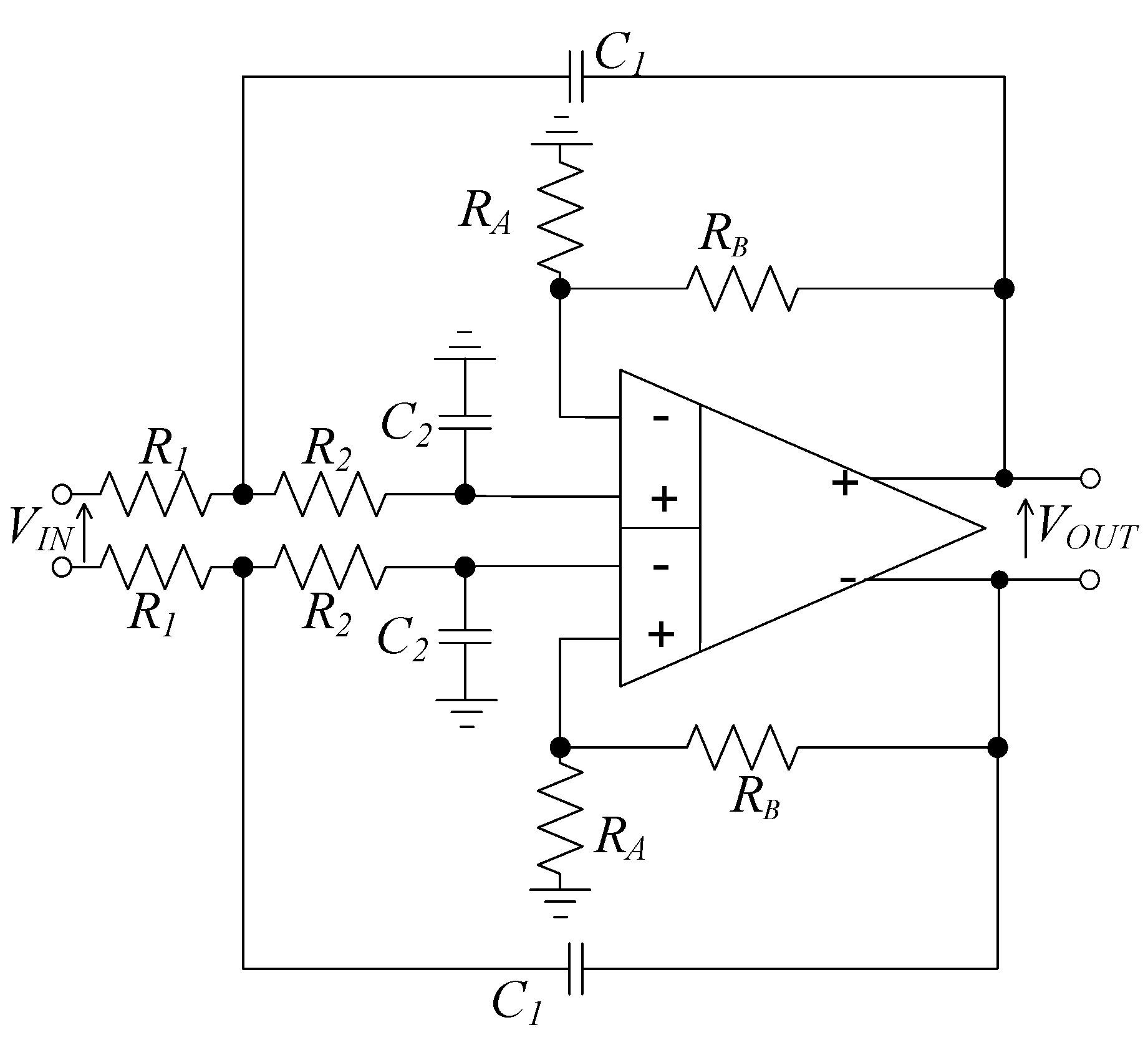
2. Proposed Biquad Architecture

Figure 1 shows the proposed fully differential topology of the Sallen–Key (SK) lowpass biquad stage based on a differential difference amplifier (DDA). The DDA can be considered a fully differential amplifier with two differential input pairs. SK filters have two feedback loops: negative feedback is used to determine the low-frequency gain, and positive feedback allows us to determine the frequency response, thanks to the feedback network formed by capacitors C 1 and C 2 and the two resistors R 1 and R 2 .
The transfer function of the circuit in Figure 1, assuming an ideal DDA, can be easily computed as:
V o u t V i n = G C 1 C 2 R 1 R 2 s 2 + ( 1 R 1 C 1 + 1 R 2 C 1 + 1 G R 2 C 2 ) s + 1 C 1 C 2 R 1 R 2
G = 1 + R B R A
Hence, the quality factor and resonance frequency of the lowpass filter are:
{ f 0 = 1 2 π C 1 C 2 R 1 R 2 Q = C 1 C 2 R 1 R 2 R 2 C 2 + R 1 C 2 + R 1 C 1 ( 1 G )
From (2), it can be seen that the value of pole Q is dependent on the value of the gain G and typically the amplifier in the SK stage is configured to have a DC gain G larger than 1 to relax the ratio of passive components when high Q is needed. If unity gain of the filter is a requirement, then resistance R 1 can be split into two resistances forming a voltage divider (with gain 1/G <1), thus reducing the gain from G   > 1 to G   = 1. However, the drawback of such a design choice is that the larger closed-loop gain limits the bandwidth of the amplifier. Therefore, the main reason to choose G = 1 is to maximize the closed-loop bandwidth of the DDA, which is necessary to obtain an accurate frequency response for the SK filter up to very high frequencies. Even if unity-gain feedback limits the maximum quality factor that can be achieved for a given ratio of passive components, a low- Q filter synthesis approach [15,16] can be used to synthesize high order filters with limited values for the Q of the biquad stages (typically in the range of 2 to 3). This results in an accurate frequency response and has the additional advantage of reducing the sensitivity and allowing a more robust design under PVT and mismatch variations.
The filter architecture for G = 1 is reported in Figure 2, where the DDA amplifier has been configured as a fully differential closed loop voltage follower.
The ideal frequency response of the SK stage in Figure 2 is
V o u t V i n = 1 C 1 C 2 R 1 R 2 s 2 + ( 1 R 1 C 1 + 1 R 2 C 1 ) s + 1 C 1 C 2 R 1 R 2
The resonance frequency and quality factor of the biquad stage can be expressed as:
{ f 0 = 1 2 π R 1 R 2 C 1 C 2 Q = C 1 C 2 R 1 R 2 R 1 + R 2
The maximum Q value is achieved for R 2 = R 1 = R , hence this choice is optimal for achieving maximum Q = 1 2 C 1 C 2 .
It is important to point out that the closed loop architecture of the SK filter results in a resonance frequency and a quality factor which are ideally independent on the parameters of the active devices and depend only on the value of the passive components.
The quality factor is, under ideal conditions, stable under process and temperature variations, because it is given by the ratio between two capacitors. The resonance frequency, instead, varies with process and temperature conditions, as it is inversely proportional to variations in resistor and capacitor values. In particular, it can be easily shown that the sensitivity of the cut-off frequency of the SK biquad to each one of the parameters R1, R2, C1 and C2 is equal to −1/2, and therefore the variations of the value of integrated passive components results in a corresponding variation of the resonance frequency. However, it has to be noted that the resonance frequency can be easily tuned implementing capacitances C 1 and C 2 with varactor-diodes or tunable MOS capacitors, and the tuning voltage of variable capacitors can be used in a servo-loop or in an automating tuning loop to accurately set the value of the cut-off frequency.
{ f 0 = 1 2 π R C 1 C 2 Q = 1 2 C 1 C 2

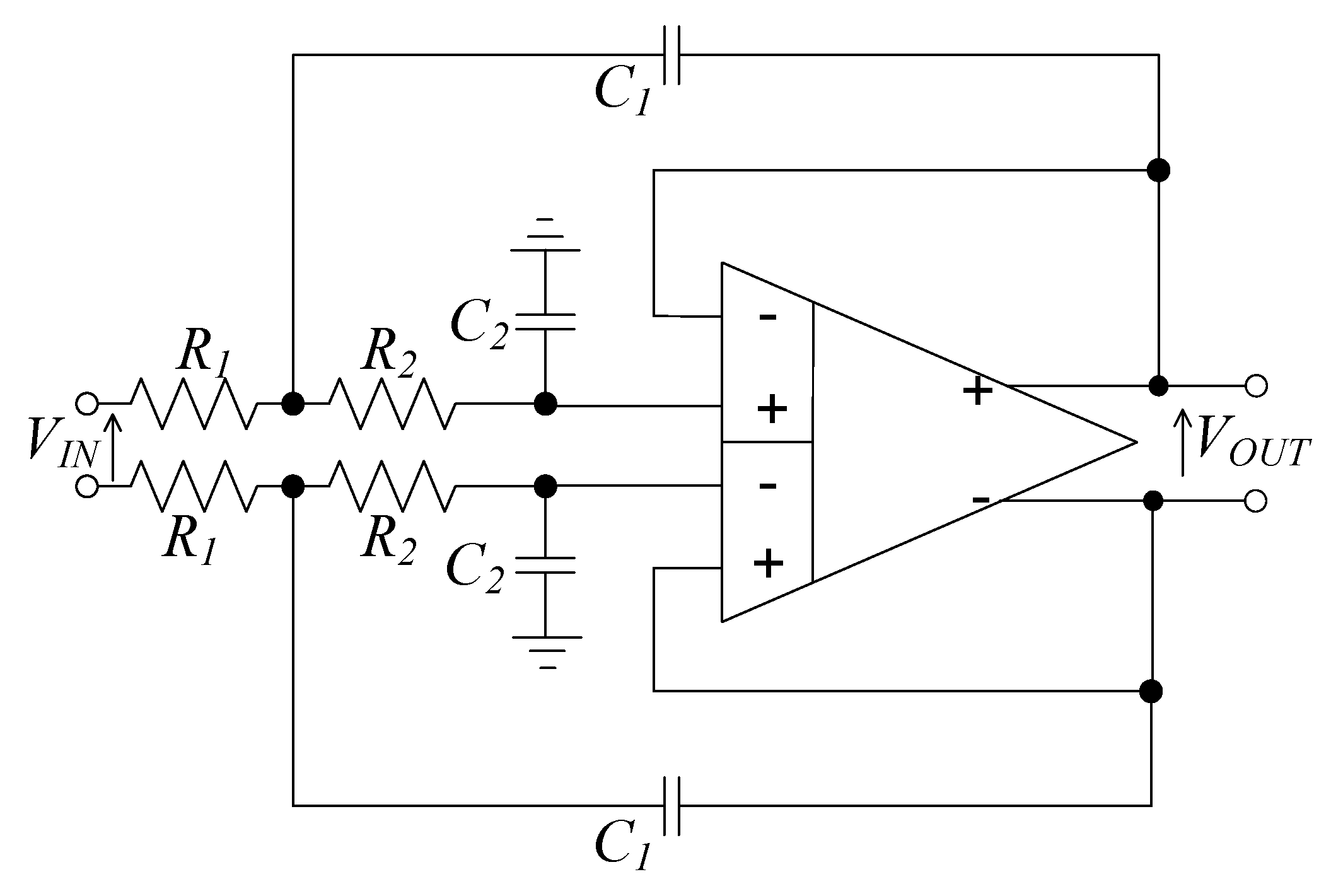
3. Proposed Topology for the DDA amplifier

In a single-ended implementation, the use of an opamp in non-inverting configuration allows applying both negative feedback to set the DC gain, and positive feedback to determine the frequency response. Mapping this approach to a fully differential implementation requires the use of a DDA, to make both the inverting and non-inverting differential input terminals available, whereas a standard fully differential opamp only allows the inverting configuration to be used.
Figure 3 shows the topology of the DDA used in the proposed SK biquad stage, where the different devices available in the technology have been exploited to maximize the performance: a single-stage DDA amplifier topology with output buffers (implemented as common collector stages) has been adopted to maximize the bandwidth, so to avoid the use of compensation capacitors; a common-mode feedback (CMFB) is also required, to set the output DC voltage and maximize the common-mode rejection ratio (CMRR).

3.1. DDA Amplifier

Referring to Figure 3, the single-stage DDA amplifier with active loads which has been used to implement the proposed biquad filter can be described as follows: high-speed npn HBT devices have been adopted for the input differential pairs (Q1-Q4), in order to exploit their high transconductance for a given current and outstanding frequency performance. RF PMOS transistors have been exploited as active loads to boost the DC gain without a significant frequency penalty. In the preliminary design phase, both resistive and active PMOS loads have been considered: however, when adopting a resistive load, the maximum allowed load resistance value is limited by the maximum allowable voltage drop across the resistors, and for the target supply voltage V C C = 3   V the gain would have been too low to guarantee enough loop gain with a single amplifier stage. Furthermore, the good frequency performance of 55-nm PMOS devices results in a limited bandwidth penalty of the active load with respect to the resistive case, guaranteeing a very large gain-bandwidth product for the DDA. The output DC voltage and swing of the stage allows keeping the source-drain voltage of transistors M1 and M2, whose biasing voltage VBP is generated by a conventional current mirror (not shown in Figure 3), below the safe limits imposed by the technology. This, however, requires a level shift to have an output DC voltage of the opamp compatible with the input DC common-mode range of the DDA.
The output stage is needed both as level shifter and to provide a very low output resistance: this is a critical issue in the design of SK filter stages, since the finite output resistance of the main active element of the filter reduces the maximum available quality factor. From this point of view, the implementation of the main active element of the SK filter as a closed loop voltage follower is advantageous, since it allows reducing the already low output resistance of the common collector stages.
In fact, remembering that the maximum Q is achieved for R 2 = R 1 = R as discussed in Section 2, considering an output resistance of the closed loop DDA amplifier R o = ϵ R , and assuming a capacitance ratio α C 2 / C 1 , the maximum achievable quality factor for the Sallen–Key stage can be rewritten as:
Q Q M A X = 1 + ϵ 8 ϵ 1 8 ϵ
Hence, even the value Q = 2 is difficult to obtain, because it would require R o < R / 32 .
In order to reduce R o , high-speed HBT devices Q5 and Q6 have been used as common collector output buffers due to the large transconductance of bipolar devices. Q5 and Q6 are biased by current sources implemented with high-voltage HBT devices (Q9 and Q10) – the reference branch of the conventional current mirror that sets the bias voltage VB1 is not shown in Figure 3. To keep the collector-emitter voltage of the high-speed HBTs below the safe limits, a common-mode level shifter, implemented through the diode-connected transistor Q11, has been exploited to reduce the collector voltage of Q5 and Q6. The use of a common-collector output stage is fundamental both to set the correct DC levels and to reduce the output resistance; however, the base-emitter Cπ capacitance introduces a zero in the transfer function that impacts on the out-of-band behavior of the lowpass filter. To compensate this effect, cross-coupled capacitors CZ1 and CZ2 have been added, exploiting the fully differential nature of the stage to cancel out the effect of the Cπ by means of positive feedback.
Neglecting r 0 , C μ , r π in the device model and assuming a capacitive load C L , the transfer function of the emitter follower with the cross-coupled capacitances is:
v o v i = 1 + s C π C Z 1 , 2 g m 1 + s C L + C π + C Z 1 , 2 g m
Hence, for C π = C Z 1 , 2 , the zero disappears, and the common collector stage only adds a pole to the transfer function, that in the limit of a large load capacitance (CL >> Cπ) results practically unaffected by the compensation capacitor.

3.2. Common Mode Feedback Loop
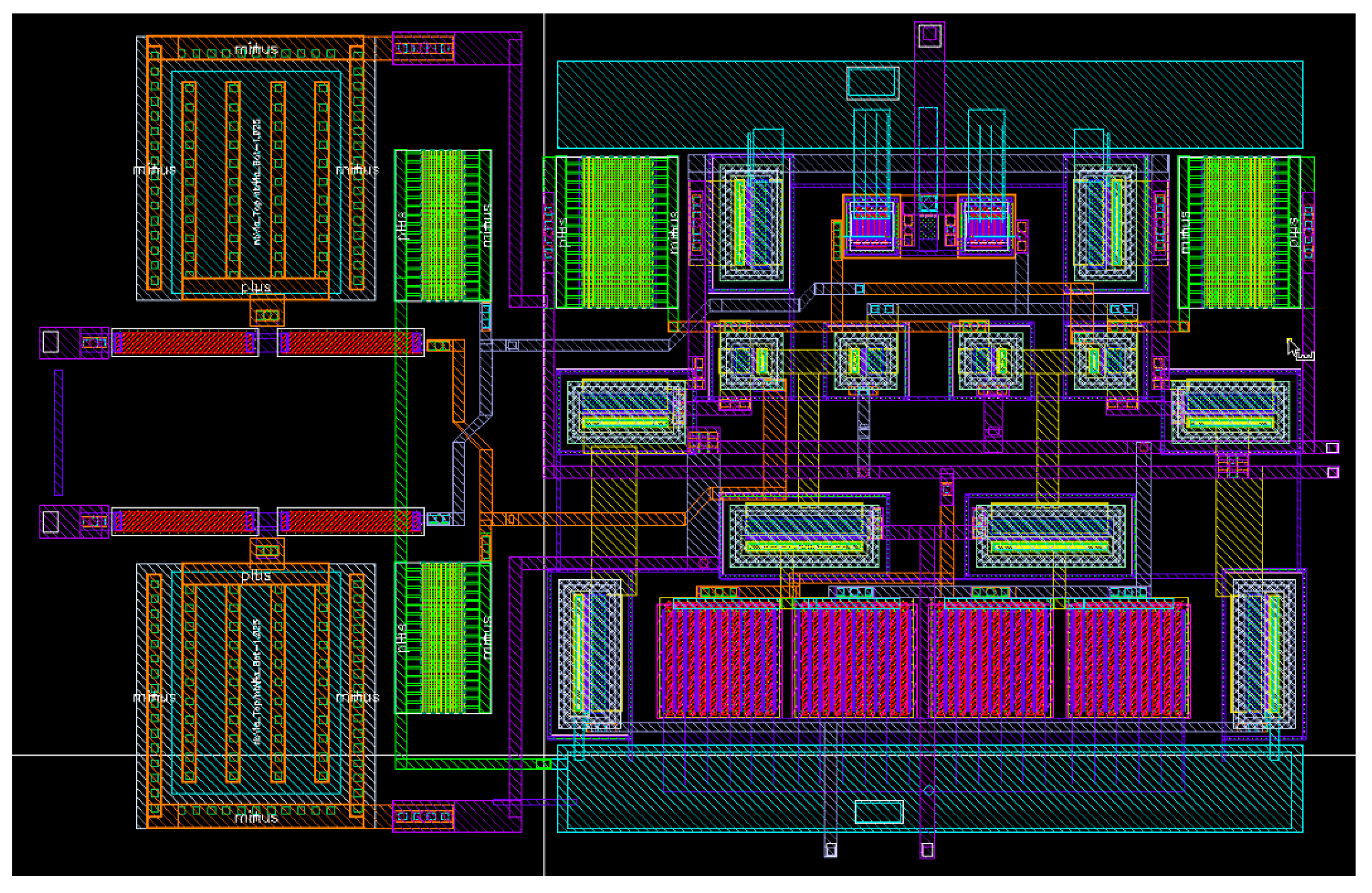
A fully differential amplifier requires a common-mode feedback (CMFB) loop to set the output DC voltage and improve the common-mode rejection ratio (CMRR). In this case, a standard triode-based CMFB has been adopted: triode degeneration has been added to the current mirror that sets the current of the DDA, formed by Q7, Q8 and Q12. The triode devices on the reference branch (M7 and M8) are controlled by the reference voltage (in this case, VREF = VCC/2), and the devices under the differential pairs (M3-M6) are controlled by the output voltages. These devices act as voltage-controlled resistors, thus adjusting the tail current of the differential pairs to match the current of the PMOS loads while setting the required output common mode voltage. Thick oxide MOS devices have been used to withstand the full swing of the output DC voltage, and their size has been optimized as a trade-off between output loading and functionality of the CMFB under PVT variations.

4. Filter Design

Unity-gain feedback and finite output conductance in the DDA, besides other non-ideal effects, limit the maximum achievable quality factor of the SK biquad stages. This is an important issue to cope with when adopting conventional filter synthesis techniques, because the maximum quality factor increases with the order of the filter, even in relatively low- Q designs such as Butterworth filters. Hence, non-conventional design approaches are required. In these approaches, a maximum Q value is chosen, and a filter mask is synthetized subject to this constraint. Unlike in conventional approaches, a larger number of biquad stages may be required for the same stopband attenuation. When adopting these methodologies, the maximum Q allowed for the biquad stages is typically in the range from 2 to 3 [15,16]: these values of Q are compatible with the biquad design proposed in this work.
The reduced Q value also reduces sensitivity to process and mismatch variations and to parasitic effects, as they increase for large quality factors: with lower quality factors, the frequency response is less dependent on variations in Q and f 0 , resulting in a more robust design with respect to process, temperature, and mismatch variations.
The proposed filter has been designed in the SiGe BiCMOS055 technology from STMicroelectronics [17], which provides high speed, heterojunction bipolar npn transistors with values of fT in excess of 300 GHz and an fMAX in excess of 350 GHz, and RF NMOS and PMOS devices with values of fT of about 190 GHz and 95 GHz, respectively. High voltage bipolar and MOS transistors with reduced frequency performance are also available to implement current sources and biasing circuits.
The biquadratic filter has been designed for a resonance frequency f 0 = 6.4   GHz and a quality factor Q = 2 , as the basic building block of a low- Q higher order filter for anti-aliasing applications in high-speed digitizers [4,5]. A resonant frequency of 6.4 GHz is ideally equivalent to a 3-dB bandwidth ( f 3 d B ) of 10 GHz for Q = 2 .
Table 1 shows the device sizing and bias current of all the bipolar and MOS transistors of the circuit in Figure 3, whereas the values of filter components (referring to Figure 2) have been set as follows: R1 = R2 = 100 Ω, C1 = 380 fF, C2 = 40 fF, CZ1 = CZ2 = 50 fF. R1 and R2 have been implemented as poly-silicon resistors, and capacitances have been implemented as MIM (metal-insulator-metal) capacitors available in the RF library of the adopted technology.
The layout of the filter is reported in Figure 4: the filter occupies an area of only 65 × 42 μm2.

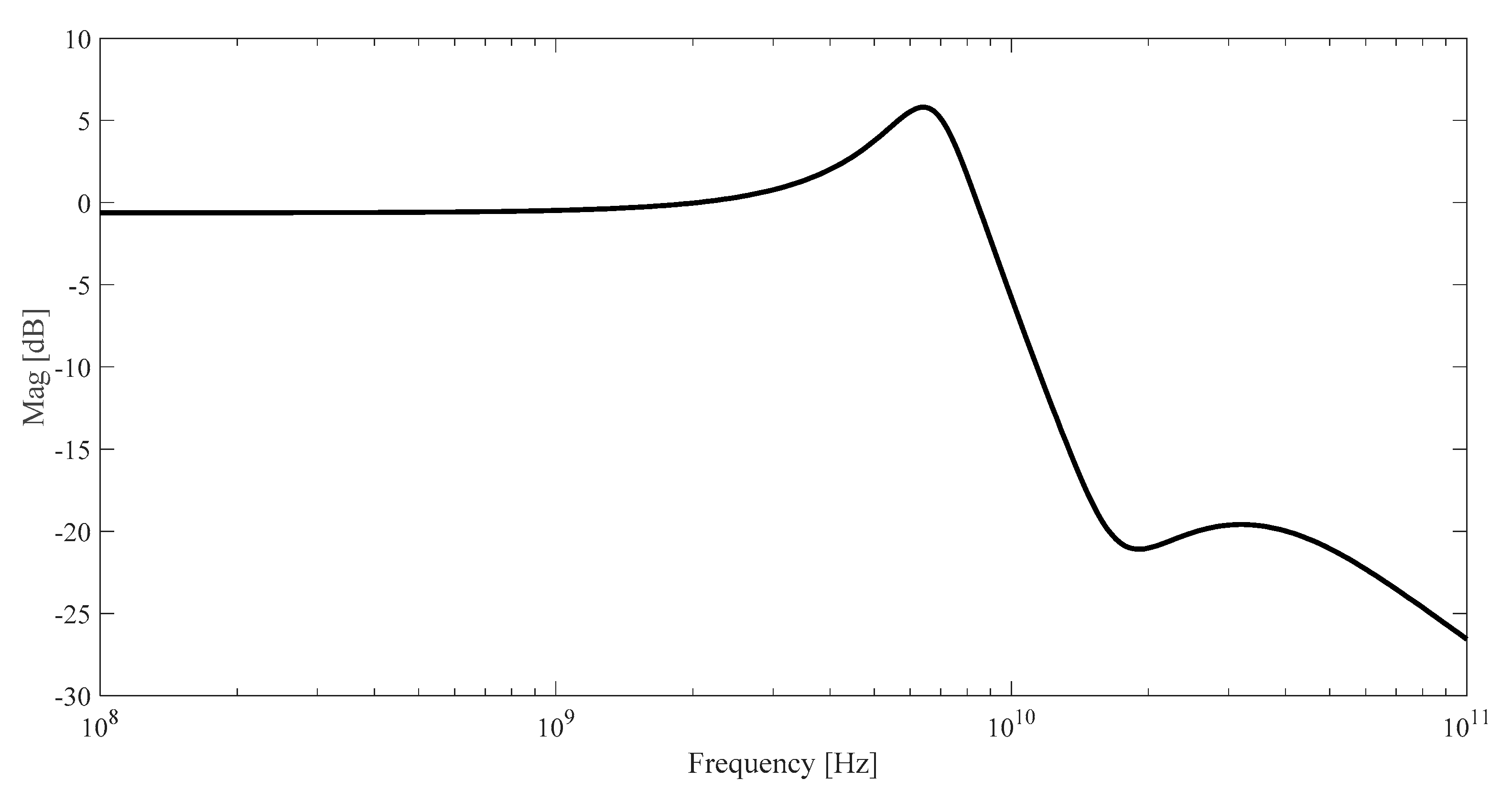
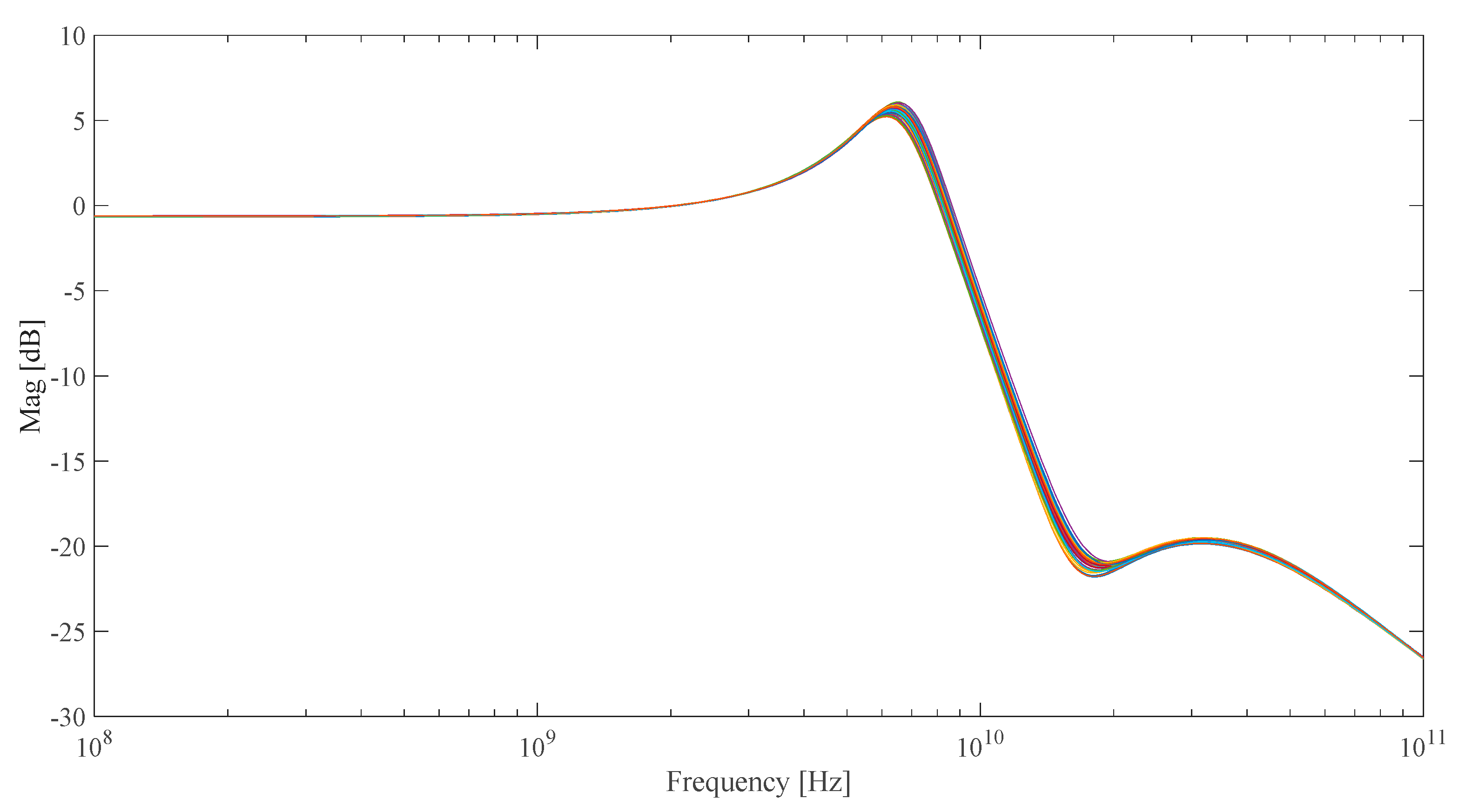
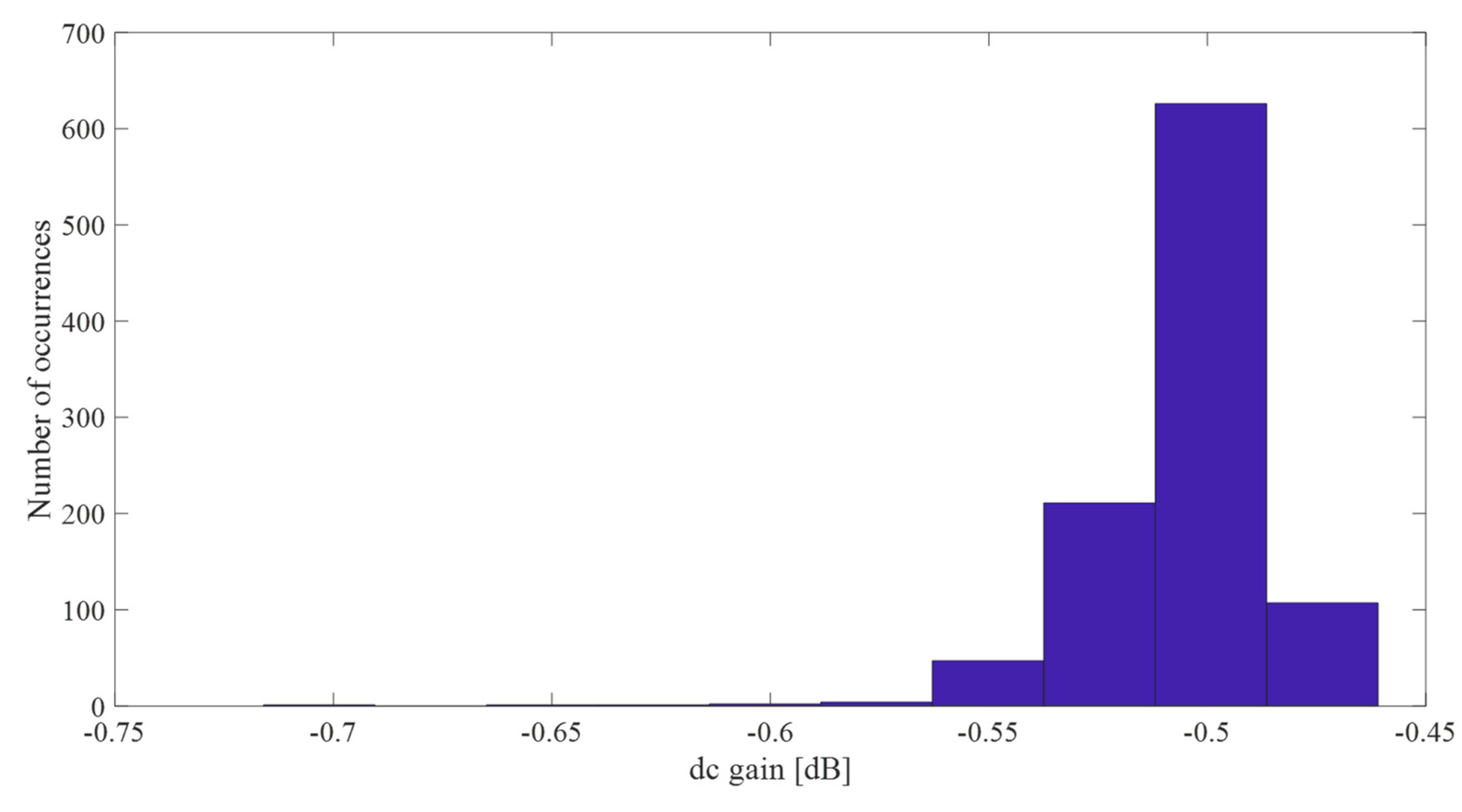
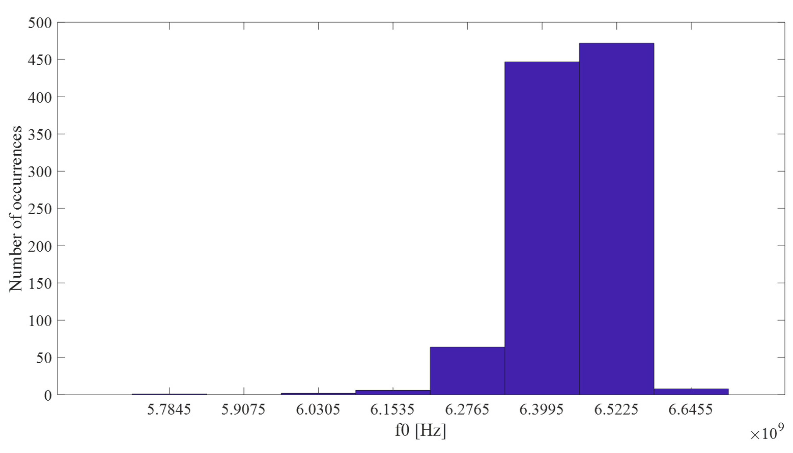
5. Simulation Results

Table 2 shows simulation results for the typical process corner and temperature (T = 27 °C). The three FOMs reported in Table 2 are defined as follows:
F O M 1 = P d i s s N p o l e
F O M 2 = P d i s s N p o l e f 3 d B
F O M 3 = P d i s s N p o l e f 3 d B D R
where N p o l e , and D R denote the number of poles (e.g., the order) and the dynamic range (computed as in [14]) of the filter respectively.
Figure 5 shows the frequency response of the filter. The Discrete Fourier Transform (DFT) of the differential output voltage with an input tone at 1 GHz, 0.8Vpp differential is reported in Figure 6.
The DFT result reported in Figure 6 demonstrates that linearity is very good, with 64 dB SFDR in the relatively large input signal condition of 800 mVpp. The dynamic range is dominated by noise, as SFDR is much better than SNR (see Table 2).
Table 3 shows the results of the simulations accounting for temperature variations, and Table 4 shows those accounting for supply voltage variations. These results confirm the robustness of the filter to both temperature and supply voltage variations.
Monte Carlo simulations, using the accurate statistical models for HBT, MOS and passive devices available in the design kit of the BiCMOS055 technology, have been carried out in the Cadence Virtuoso ADE XL environment. Figure 7 shows the frequency response of the biquad filter for 100 Monte Carlo iterations, whereas Figure 8, Figure 9, Figure 10 and Figure 11 show the histograms of DC gain, quality factor, resonant frequency and 3 dB bandwidth of the filter respectively. A summary of the mean values ( μ ) and standard deviations ( σ ) for these quantities is reported in Table 5.
All these results allow us to assess the robustness of the filter under Monte Carlo simulations: the DC gain is almost constant, while the quality factor and resonance frequency of the complex poles vary limitedly.
A comparison with recent technical papers reporting inductorless active lowpass filters with cut-off beyond 1.5 GHz and the proposed filter is reported in Table 6. The proposed filter outperforms all the other designs in terms on SFDR, DR and FOM3, confirming the outstanding linearity performance of our unitary-gain, closed-loop approach.
It has to be noted that most papers in the literature are based on the Gm-C approach [11,12,18,19], in which the open-loop input stage often limits linearity, whereas the closed loop approach proposed in this work exploits feedback to reduce nonlinear distortions. Focusing on reference [8], it is based on a closed loop Tow–Thomas (TT) architecture which shows a limited dynamic range owing to the lower bandwidth of CMOS amplifiers, which makes feedback less effective. Reference [14] exploits positive feedback to synthetize an active inductor (AL), and resistive degeneration of the differential pair to improve linearity. Having similar performance and using the same technology, this solution shows lower power consumption but also lower dynamic range; hence, it performs better in the first two FOMs, but worse in the third-one, owing both to worse SNR and SFDR performance. Reference [13] reports a 5th-order filter based on an active circuit which provides a transfer function with two poles and two zeros with only three active devices: this provides for very good power efficiency, as shown by excellent FOM1 and FOM2 performance, but no detailed noise information is provided, so FOM3 cannot be computed. As it reports 100nV/√Hz noise for 4.57 GHz of bandwidth, estimated noise is 6.8 mV, which would provide a very low SNR of 25.5 dB. Hence, the dynamic range of such a design is severely limited.

6. Conclusions

A fully differential Sallen–Key filter with a 3-dB bandwidth of about 10 GHz and based on a DDA amplifier which exploits bipolar and MOS devices of the commercial BiCMOS055 technology from STMicroelectronics has been proposed in this work. Post-layout simulations have shown that the proposed filter outperforms all recently published inductorless active lowpass filters with cut-off frequencies beyond 1.5 GHz in terms of SFDR, DR, and FOM3. Parametric simulations accounting for temperature and supply voltage variations as well as Monte Carlo simulations have confirmed the robustness of the filter to temperature, supply voltage and mismatch variations. The power efficiency of the proposed filter is good and the area footprint is very low. Based on the comparison against the state of the art reported in Table 6, we have demonstrated that the proposed architecture—which exploits a fully differential DDA-based voltage follower as active element—allows the implementation of closed loop biquad filters with a 3-dB bandwidth up to about 10 GHz while guaranteeing better linearity performance with respect to filter architectures based on the Gm-C or the active inductor approach. Furthermore, we can state that it is possible to use the proposed fully differential Sallen–Key closed-loop topology for filters with bandwidths around 10 GHz, exploiting NPN devices with an f T in the order of 300 GHz and PMOS with an f T in the order of 100 GHz as active loads. Unity gain feedback across the DDA ensures the highest closed-loop bandwidth, though limiting the achievable maximum quality factor. The resulting filter is also compact, and shows the lowest area occupation among the existing literature.

Author Contributions

Conceptualization, G.S. and A.T.; methodology, F.C. and P.M.; software, P.T.; validation, F.C., P.M. and G.S.; formal analysis, P.M.; investigation, F.C.; resources, A.T.; writing—original draft preparation, G.S.; writing—review and editing, P.T., F.C. and P.M.; funding acquisition, A.T. All authors have read and agreed to the published version of the manuscript.

Funding

This work is supported by European ECSEL-JU/EU-H2020 under grant no. 737454.

Conflicts of Interest

The authors declare no conflict of interest.

References

  1. Kim, S.-N.; Kim, W.-C.; Seo, M.-J.; Ryu, S.-T. A 65-nm CMOS 6-Bit 20 GS/s Time-Interleaved DAC With Full-Binary Sub-DACs. IEEE Trans. Circuits Syst. II Express Briefs 2018, 65, 1154–1158. [Google Scholar] [CrossRef]
  2. Zandieh, A.; Schvan, P.; Voinigescu, S.P. Design of a 55-nm SiGe BiCMOS 5-bit Time-Interleaved Flash ADC for 64-Gbd 16-QAM Fiberoptics Applications. IEEE J. Solid-State Circuits 2019, 54, 2375–2387. [Google Scholar] [CrossRef]
  3. Sun, K.; Wang, G.; Zhang, Q.; Elahmadi, S.; Gui, P. A 56-GS/s 8-bit Time-Interleaved ADC With ENOB and BW Enhancement Techniques in 28-nm CMOS. IEEE J. Solid-State Circuits 2018, 54, 821–833. [Google Scholar] [CrossRef]
  4. Monsurrò, P.; Trifiletti, A.; Angrisani, L.; D’Arco, M. Streamline calibration modelling for a comprehensive design of ATI-based digitizers. Measurement 2018, 125, 386–393. [Google Scholar] [CrossRef]
  5. Monsurrò, P.; Trifiletti, A.; Angrisani, L.; D’Arco, M. Two novel architectures for 4-channel mixing/filtering/processing digitizers. Measurement 2019, 142, 138–147. [Google Scholar] [CrossRef]
  6. Chen, Y.; Mak, P.-I.; Wang, Y.; Zhang, L.; Qian, H. 0.013 mm2, kHz-to-GHz-bandwidth, third-order all-pole lowpass filter with 0.52-to-1.11 pW/pole/Hz efficiency. Electron. Lett. 2013, 49, 1340–1342. [Google Scholar] [CrossRef]
  7. Wambacq, P.; Giannini, V.; Scheir, K.; Van Thillo, W.; Rolain, Y. A fifth-order 880MHz/1.76GHz active lowpass filter for 60GHz communications in 40nm digital CMOS. In Proceedings of the ESSCIRC 2010—36th European Solid State Circuits Conference, Seville, Spain, 14–19 September 2010; pp. 350–353. [Google Scholar]
  8. Wu, C.-D.; Hsieh, J.-Y.; Wu, C.-H.; Cheng, Y.-S.; Wu, C.-C.; Lu, S.-S. An 1.1 v 0.1–1.6 GHz tunable-bandwidth elliptic filter with 6 dB linearity improvement by precise zero location control in 40 nm CMOS technology for 5G applications. In Proceedings of the 2017 IEEE International Symposium on Circuits and Systems (ISCAS), Baltimore, MD, USA, 28–31 May 2017. [Google Scholar]
  9. Salem, S.B.; Fakhfakh, M.; Masmoudi, D.S.; Loulou, M.; Loumeau, P.; Masmoudi, N. A high performances CMOS CCII and high frequency applications. Analog. Integr. Circuits Signal Process. 2006, 49, 71–78. [Google Scholar] [CrossRef]
  10. Safari, L.; Barile, G.; Ferri, G.; Stornelli, V. High performance voltage output filter realizations using second generation voltage conveyor. Int. J. RF Microw. Comput. Eng. 2018, 28, e21534. [Google Scholar] [CrossRef]
  11. Lu, Y.; Krithivasan, R.; Kuo, W.-M.L.; Li, X.; Cressler, J.D.; Gustat, H.; Heinemann, B. A 70 MHz–4.1 GHz 5th-order elliptic gm-C low-pass filter in complementary SiGe technology. In Proceedings of the 2006 Bipolar/BiCMOS Circuits and Technology Meeting, Maastricht, The Netherlands, 8–10 October 2006. [Google Scholar]
  12. Houfaf, F.; Egot, M.; Kaiser, A.; Cathelin, A.; Nauta, B. A 65nm CMOS 1-to-10GHz tunable continuous-time low-pass filter for high-data-rate communications. In Proceedings of the 2012 IEEE International Solid-State Circuits Conference, San Francisco, CA, USA, 19–23 February 2012; pp. 362–363. [Google Scholar]
  13. Xiao, H.; Schaumann, R. Very-high-frequency lowpass filter based on a CMOS active inductor. In Proceedings of the 2002 IEEE International Symposium on Circuits and Systems, Phoenix-Scottsdale, AZ, USA, 26–29 May 2002. [Google Scholar]
  14. Centurelli, F.; Monsurrò, P.; Trifiletti, A. A 10 GHz inductorless active SiGe HBT lowpass filter. Int. J. RF Microw. Comput. Eng. 2018, 28, e21567. [Google Scholar] [CrossRef]
  15. Monsurrò, P.; Pennisi, S.; Scotti, G.; Trifiletti, A. Design strategy for biquad-based continuous-time low-pass filters. In Proceedings of the 20th European Conference on Circuit Theory and Design, Linkoping, Sweden, 29 August 2011; pp. 385–388. [Google Scholar]
  16. Monsurrò, P.; Pennisi, S.; Scotti, G.; Trifiletti, A. High-tuning-range CMOS band-pass IF filter based on a low-Qcascaded biquad optimization technique. Int. J. Circuit Theory Appl. 2014, 43, 1615–1636. [Google Scholar] [CrossRef]
  17. Chevalier, P.; Avenier, G.; Canderle, E.; Montagné, A.; Ribes, G.; Vu, V.T. Nanoscale SiGe BiCMOS technologies: From 55 nm reality to 14 nm opportunities and challenges. In Proceedings of the 2015 IEEE Bipolar/BiCMOS Circuits and Technology Meeting – BCTM, Boston, MA, USA, 26–28 October 2015. [Google Scholar]
  18. Sabatino, N.; Minoia, G.; Roche, M.; Baldi, D.; Temporiti, E.; Mazzanti, A. A 5th Order gm-C Low-Pass Filter with ±3% Cut-Off Frequency Accuracy and 220 MHz to 3.3 GHz Tuning-Range in 28nm LP CMOS. In Proceedings of the IEEE European Solid State Circuits Conference, ESSCIRC 2014, Venice Lido, Italy, 22–26 September 2014; pp. 351–354. [Google Scholar]
  19. Baranauskas, D.; Zelenin, D.; Bussmann, M.; Elahmadi, S.; Edwards, J.K.; Gill, C.A. A 1.6-3.2-GHz sixth-order +13.1-dBm OIP3 linear phase gm-C filter for fiber-optic EDC receivers. IEEE Trans Microw Theory Tech. 2010, 58, 1314–1322. [Google Scholar] [CrossRef]
Figure 1. Architecture of the proposed lowpass biquadratic filter.
Electronics 09 00563 g001
Figure 2. Architecture of the proposed lowpass filter with DDA configured as voltage follower.
Electronics 09 00563 g002
Figure 3. Proposed topology for the DDA amplifier with fully differential output.
Electronics 09 00563 g003
Figure 4. Layout of the proposed Biquad Filter.
Electronics 09 00563 g004
Figure 5. Frequency Response of the proposed Biquadratic Filter.
Electronics 09 00563 g005
Figure 6. Discrete Fourier Transform (DFT) of the differential output voltage with an input tone at 1GHz, 0.8Vpp differential.
Electronics 09 00563 g006
Figure 7. Frequency Response for 100 Monte Carlo iterations.
Electronics 09 00563 g007
Figure 8. Histogram of DC Gain A d c for 1000 Monte Carlo iterations.
Electronics 09 00563 g008
Figure 9. Histogram of quality factor Q for 1000 Monte Carlo iterations.
Electronics 09 00563 g009
Figure 10. Histogram of resonant frequency f 0 for 1000 Monte Carlo iterations.
Electronics 09 00563 g010
Figure 11. Histogram of 3 dB bandwidth f 3 d B for 1000 Monte Carlo iterations.
Electronics 09 00563 g011
Table 1. Device sizing.
DeviceSizeBias Current
Q1, Q2, Q3, Q4 L e / W e   1 = 1 / 0.2   μ m IC = 1 mA
Q5, Q6 L e / W e = 4 / 0.2   μ m IC = 1 mA
Q7, Q8,Q12 L e / W e = 5 / 0.2   μ m IC = 1 mA
Q9, Q10 L e / W e = 5 / 0.2   μ m IC = 1 mA
Q11 L e / W e = 2 × 4 / 0.2   μ m IC = 1 mA
M1, M2W/L = 6/0.06 μ m ID = 1 mA
M3,M4,M5,M6W/L = 20/0.25 μ m ID = 1 mA
1 L e / W e = Emitter Length/Emitter Width
Table 2. Typical 27 °C simulations.
NameValueUnitNotes
P d i s s 18mWPower Dissipation
V c c 3VSupply Voltage
f 0 6.45GHzResonant Frequency
f 3 d B 9.55GHz3 dB Bandwidth
A D C −0.5dBDC-Gain
A P K 5.8dBPeak Gain
Q 2.06-Quality Factor
SFDR64dB@0.8Vpp differential,1 GHz
v o n o i s e 1.36mVrmsOutput Noise integrated between 1 Hz and 10 GHz
SNR46.4[ dB ] @0.8Vpp differential
D R   149.3dBDynamic Range
FOM19mW
FOM20.94pW/Hz
FOM30.0032mW/GHz
1 DR has been computed as in [14].
Table 3. Simulations vs. temperature.
NameMinimumMaximumUnit
T −30120°C
P d i s s 18.419.56mW
f 0 6.915.65GHz
f 3 d B 10.28.2GHz
A p k 5.515.3dB
A d c −0.53−0.58dB
Q 21.9-
SFDR6173dB
v o n o i s e 1.121.51mV
D R 149.451.6dB
1 DR has been computed as in [14].
Table 4. Simulations vs. supply voltage.
NameValueValueUnit
V c c 2.853.15V
P d i s s 17.119.9mW
f 0 6.16.4GHz
f 3 d B 8.99.6GHz
A p k 4.895.72dB
A d c −0.7−0.56dB
Q 1.92-
SFDR4856dB
v o n o i s e 1.261.26mV
D R 144.347dB
1 DR has been computed as in [14].
Table 5. Summary of Monte Carlo simulations (1000 iterations).
Name μ σ Unit
A d c −0.5050.018dB
Q 2.0710.037-
f 0 6.4710.100GHz
f 3 d B 9.5880.126dB
Table 6. Comparison against the state of the art.
This Work[14][8][18][12][19][11][13]
Year20202018201720142012201020062002
TechnologyBiCMOS
55 nm
BiCMOS
55 nm
CMOS
40 nm
CMOS
28 nm
CMOS
65 nm
BiCMOS
180 nm
BiCMOS
250 nm
CMOS
180 nm
Filter TypeSKALTTGMCGMCGMCGMCAL
Supply Voltage [ V ] 331.11.11.43.33.51.8
P diss [ mW ] 1813.717.63014030099.81.6
f 3 dB [ GHz ] 9.5510.51.63.3103.24.14.6
SFDR [ dB ] )64−51−46−40−4540-−57
v onoise [ mVrms ] 1.361.11.5-0.5---
SNR [ dB ] 46.447.243.23945---
D R 1 [ dB ] 49.345.541.13742-20.1-
Npole22553655
FOM1 [ mW ] 96.853.52646.65019,90.32
FOM2 [ pW / Hz ] 0.940.652.21.814.715.64,80.07
FOM3[ mW / GHz ] 0.00320.00350.0190.0250.037-0.47-
Area (mm2)0.00270.00560.120.0910.010.170.82-
MeasuredNoNoYesYesYesNoYesYes
1 DR has been computed as in [14].

