Abstract
The present work proposes a 180–225 GHz broadband frequency doubler monolithic microwave integrated circuit (MMIC) based on a novel Schottky barrier diode (SBD) terminal structure denoted as a Schottky metal-brim (SMB). Compared with an MMIC adopting the conventional SBD terminal structure, preliminary measurements show that the maximum output power of the MMIC adopting the SMB structure increases from 0.216 mW at 206 GHz to 0.914 mW at 208 GHz. Analysis of the nonlinear current–voltage and capacitance–voltage characteristics of the two terminal structures based on an extended one-dimensional drift-diffusion model, indicates that the SMB structure provides significantly better conversion efficiency than the conventional SBD structure by eliminating the accumulation of charge and additional current paths near the Schottky electrode edge. It provides a feasible scheme for the optimization of MMIC applications requiring high power and high efficiency.
1. Introduction
Terahertz science and technology have developed rapidly in recent decades, and this has promoted the use of THz radiation in many high-requirement applications, such as astrophysics and earth science, high-speed communication, biomedicine, and safety imaging [1,2,3]. A critical component in THz systems is electronic sources based on a local oscillator (LO) followed by a combination of amplifiers and frequency multipliers with sufficient output power [4,5]. Accordingly, the tremendous interest in THz technology has led to the development of a series of local oscillators operating in the THz band (i.e., 100 GHz to 30 THz) [6]. Among these, frequency multiplier chains based on Schottky diodes have been commonly employed due to their advantages of low cost, frequency agility, easy integration, and good functionality both at room temperature and at cryogenic temperatures [7,8,9]. Meanwhile, a number of advanced semiconductor technologies have been developed worldwide for frequency multiplier applications in the THz band. For example, Virginia Diodes Inc. (VDI), the Jet Propulsion Laboratory (JPL), and Advanced Compound Semiconductor Technologies (ACST) GmbH have already developed all-solid-state frequency multiplier monolithic microwave integrated circuits (MMICs) with high efficiency and an output power of a dozen milliwatts in the frequency range of 200–600 GHz [10,11]. In contrast, frequency multiplier research in China has mainly focused on hybrid integrated circuits with discrete Schottky diodes operating at a frequency of around 200 GHz. As such, the development of frequency multiplier MMICs based on Schottky diodes has been rarely reported in China. Among the very few examples, Ren et al. developed a 330–500 GHz broadband tripler MMIC [12]. However, the MMIC exhibited low efficiency, with an output power that was only on the order of a hundred microwatts.
Broadband frequency multipliers function at low forward and reverse biases by applying a small input signal, where the capacitance–voltage and current–voltage relationships are the dominant nonlinear terms. Conversion efficiency is an important criterion for evaluating the performance of frequency multipliers. This efficiency is affected primarily by circuit mismatching, parasitic parameters, increasing resistance, and the power saturation effect. The fact that Schottky diodes form the core device of frequency multipliers suggests that efforts to increase the power output and efficiency of broadband frequency multipliers should focus on increasing the efficiency of Schottky diodes.
The present work addresses the above-discussed issues by developing a 180–225 GHz broadband frequency doubler MMIC based on a novel Schottky barrier diode (SBD) terminal structure denoted as Schottky metal-brim (SMB). Preliminary measurement results demonstrate that the maximum efficiency and maximum output power of an MMIC adopting the proposed SMB structure are 8.39% and 0.92 mW, respectively, at 208 GHz, while those of an MMIC adopting the conventional SBD structure are 2.81% and 0.20 mW, respectively, at 212 GHz. The cause of the improved performance of the proposed SMB terminal structure is evaluated through a comparative analysis of the nonlinear current–voltage and capacitance–voltage characteristics of the two terminal structures based on an extended one-dimensional (1-D) drift-diffusion (DD) model [13]. The models were employed directly in design automation tools, such as Advanced Design System (ADS) simulation environment, to evaluate the frequency responses of the SBDs accurately.
2. Materials and Methods
The proposed SMB terminal structure is illustrated in Figure 1a, while the conventional SBD terminal structure is illustrated in Figure 1b. The proposed SBD structure is designed to eliminate the accumulation of charge and additional current paths near the Schottky electrode edge by better isolating the n-type GaAs epitaxial layer (epilayer), which is beneficial for MMIC applications requiring high power and high efficiency. We selected GaAs as a commonly used material for frequency multipliers based on Schottky diodes due to its high electron mobility and the small reverse saturation current provided by the resulting diodes. Based on our previously published studies [12,14], the diode structure was fabricated on a GaAs wafer with epitaxial lattice-matched GaAs layers, including a 1.5-μm-thick heavily doped n-type GaAs buffer epilayer with an Si doping concentration of ~1018 cm−3 and a 0.3-μm-thick lightly doped n-type GaAs epi-layer with an Si doping concentration of ~1017 cm−3.
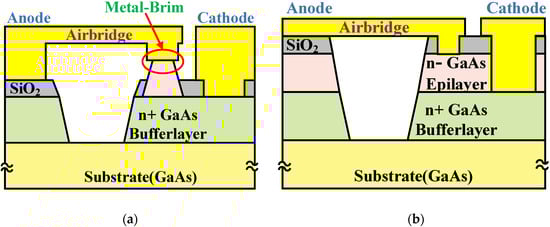
Figure 1.
Cross-sectional schematics of GaAs Schottky barrier diodes (SBDs): (a) Schottky metal-brim (SMB) terminal structure; (b) conventional terminal structure.
A scanning electron microscopy (SEM) image of a fabricated frequency doubler MMIC with the proposed SMB terminal structure is shown in Figure 2a, and the detail of the diode cell in MMIC is shown in Figure 2b. The fabrication process began with mesa isolation using wet etching. Subsequently, Schottky metal and cathode ohmic contacts were deposited by electron-beam evaporation. The metal-brim structure was then formed by specified dry etching and a planarization process. Then, a 300-nm-thick SiO2 layer was deposited by plasma-enhanced chemical vapor deposition (PECVD) for the passivation of the SMB structure, and the dielectric layer on the top of the metal contacts was removed by SF6 plasma dry etching. Next, a 1.5-μm-thick gold layer was electroplated to form the air bridge fingers and passive circuitry, such as waveguide probes and filter structures. Finally, the GaAs substrate was thinned to the desired thickness (34–37 μm) by lapping and polishing.
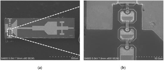
Figure 2.
SEM images: (a) a fabricated doubler monolithic microwave integrated circuit (MMIC) chip; (b) the inside diode cell structure.
3. Model Analysis
We first evaluated the reverse and forward bias DC I–V characteristics of the conventional SBD and the proposed SMB devices using an Agilent B1500 semiconductor device parameter analyzer. In addition, the extended 1-D DD model was applied for comparison with the experimental I–V results. Figure 3 presents the measured and simulated reverse and forward bias DC I–V characteristics of the two SBDs on a log scale, which has the best agreement with the measured data at larger forward bias.
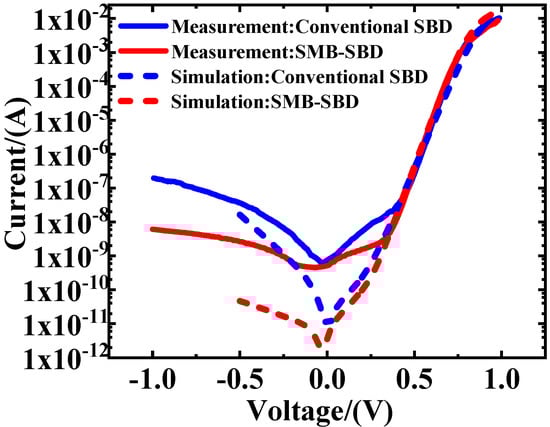
Figure 3.
Measured and simulated low reverse- and forward-biased DC I–V curves for the two SBD structures on a log scale.
However, the most striking features of the results in Figure 3 are that the measured currents of conventional SBD structure at a given bias voltage are much larger than those of SMB structure at reverse and low forward biases and that these observed deviations from ideal curve are greater for the conventional SBD structure than for the SMB terminal structure. This is not conducive to the power conversion of frequency multiplier. In addition, various parameters were extracted from the SBD devices using the Agilent B1500A system, as listed in Table 1, and were used in the simulations and for analyzing the effects of the different terminal structures on the frequency conversion efficiency of the MMICs.

Table 1.
Parameters of SBDs with different terminal structures.
Generally, the current model was based on thermionic emission theory through the Schottky contact [15]. The common I–V SPICE model used in the harmonic balance simulation is given as follows:
Here, is the reverse saturated current, , is the applied bias, is the ideal factor, is the thermal voltage, is the built-in voltage of the Schottky contact, where , and [16,17].
To explain this, we first note that random variations in the epitaxial material and processing technology result in leakage currents, which are not accounted for in Equation (1). This affects the simulation results for both SBD structures equally. Secondly, unlike the proposed SMB terminal structure, the conventional SBD terminal structure introduces an additional direct current path between the anode/depletion layer and the cathode, as illustrated in Figure 4, which is also not accounted for in Equation (1), and directly impacts the accuracy of the simulation results for the conventional SBD structure.
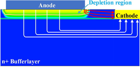
Figure 4.
Schematic illustrating the current paths in a conventional SBD structure under low forward bias conditions. White lines are thermionic emission currents, while the red lines are additional current paths between the anode depletion layer and the ohmic cathode contact.
The above analysis indicates that the SBD with the proposed metal-brim terminal structure provides measured I–V curves that conform better with the ideal model given by Equation (1) than the conventional SBD due to its elimination of Schottky fringing electric field effects that lead to an additional current path. These fringing field effects are one reason why the performances of frequency multiplier MMICs tend to deviate from their ideal design results [18]. Therefore, the I–V model of the conventional SBD must be modified to account for the additional direct current path between the anode/depletion layer and the cathode. The modified equation is given as follows:
Here, is a tunneling factor that determines the inverse breakdown characteristic of actual diodes and is a nonlinear component indicative of Schottky fringing effects. The ranges given for the first two conditions are different from those given in Equation (1). This could be explained by the tunneling current deviation from thermionic emission theory when the diode works at negative bias.
Figure 5 presents the measured and simulated reverse and forward bias DC I–V characteristics of the conventional SBD on a log scale along with the simulated curves obtained from Equations (1) and (2). We note that the curve of Equation (2) is in good agreement with the measured data under low reverse and forward bias voltages, indicating that the revised model reliably represents the I–V characteristics of the conventional SBD. Note that the method of harmonic balance was used to extract the second component of the nonlinear curve to realize the analysis of the frequency multiplier MMIC.
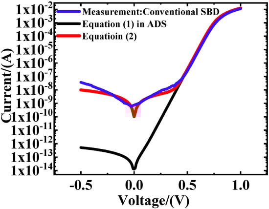
Figure 5.
Comparison of the measured reverse- and forward-biased DC I–V curves of the conventional SBD structure and simulated curves based on different models.
We also plotted the simulated C–V characteristics of the conventional SBD and the proposed SMB devices based on the ideal 1-D drift-diffusion (DD) model, as shown in Figure 6. Because the broadband doubler operates in the small signal behavior regime of the SBDs, the C–V characteristics of an SBD below the built-in voltage can be given according to the following conventional equation:
where is the area of the anode, is the dielectric constant of the semiconductor, and is the doping concentration of the epilayer. Equation (3) represents ideal conditions and completely neglects any consideration of fringing effects and interface states. We note from Figure 6 that the results of Equation (3) are in very good agreement with the simulated results of the proposed SMB device. This indicates that the SMB structure completely eliminates the depletion layer capacitance fringing effect that is evident in conventional SBDs. The depletion layer capacitance fringing effect of the conventional SBD can be accounted for through a straightforward extension of Equation (3) as follows:
where the parameters (a correction term) and (the radius of Schottky junction) are determined by the report in [19]. includes the fringing factors, and its value is 1 without considering the capacitance effect of the interface states.
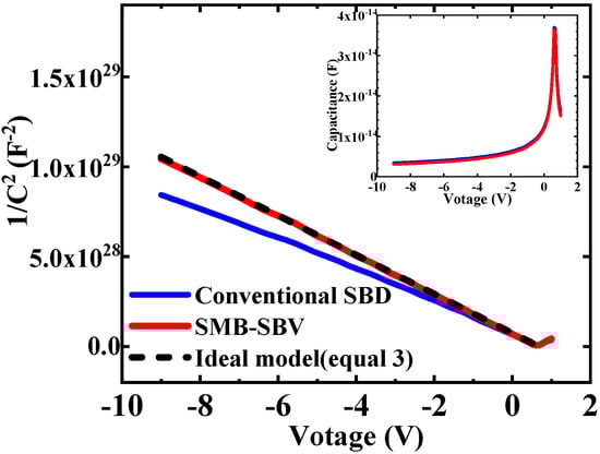
Figure 6.
Comparison between the values of 1/C2 obtained for the two different SBD structures based on 1-D DD simulations and the ideal model given in Equation (3). The simulations were based on an ideal surface potential. The inset presents the simulated C–V in linear scale.
Accordingly, the source of operating frequency current can be expressed as follows [20]:
Equation (5) indicates that the second harmonic was the result of the thermionic emission current and displacement current through the undepleted semiconductor. The symbolically defined device (SDD) component was employed to quickly and accurately analyze the effect of the SMB structure on the frequency multiplier efficiency based on the I–V and C–V characteristics of the SBDs.
4. Results
The cavity of the designed doubler is made of brass material, and the entire surface is gold-plated. The doubler MMIC is fixed and grounded by conductive adhesive, which is shown in Figure 7. The measurement setup employed for testing the frequency doubler MMICs is presented in Figure 8. Here, an Agilent E8257D analog signal generator (Santa Clara, CA, USA) was followed by a W-band, active ×8 frequency multiplier to generate an input signal in the 86–106 GHz band with a typical output power of +10 dBm. The output power of the frequency multipliers was measured using a VDI Erickson PM4 power meter (Charlottesville, VA, USA). In addition, a KFD55 Sub-Miniature version A (SMA) coaxial RF connector (Xi’an, China) was connected to the main transmission circuit using gold wire bonding, and a low forward bias (+0.8 V) was applied to the SMA port to bias the SBDs in the doubler MMICs. Two doublers based on different Schottky barrier diode (SBD) terminal structures were tested.
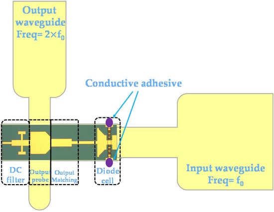
Figure 7.
The overall doubler circuit model of the wideband doubler MMIC.
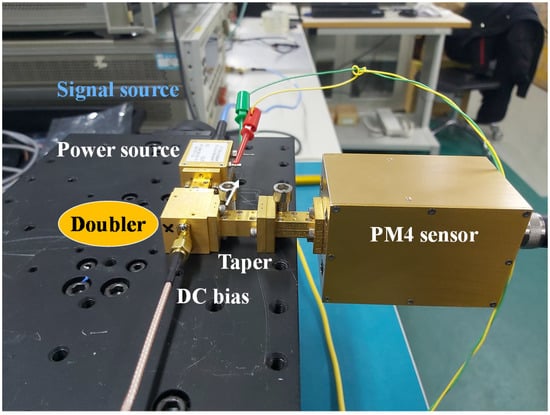
Figure 8.
Photo of measurement site for the 180–220 GHz broadband frequency doubler MMIC.
The measured output power of the frequency doubler MMICs constructed using the conventional SBD and the proposed SMB structures is shown in Figure 9a with respect to frequency along with the input power. The measured output power of the frequency doubler MMIC constructed using the proposed SMB structure is greater than 0.5 mW in the range from 188 to 208 GHz, and the maximum output power is about 0.914 mW at 208 GHz. In contrast, the maximum output power of the frequency doubler MMIC constructed using the conventional SBD structure was only 0.216 mW at 206 GHz.
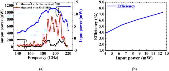
Figure 9.
(a) Measured output power of 180–220 GHz broadband frequency doubler MMICs based on the conventional SBD and the proposed SMB terminal structures with respect to frequency, along with the input power. (b) Measured efficiency of the frequency doubler MMIC based on the proposed SMB terminal structure versus input power operating at 99 GHz.
Naturally, the output power of both frequency doubler MMICs would be greater with a larger input power. Figure 9b shows the measured efficiency of the frequency doubler MMIC based on the proposed SMB terminal structure versus input power operating at 99 GHz. We note that the efficiency monotonically increases with increasing input power. The efficiency would be higher with a sufficient power source.
5. Conclusions
In summary, 180–225 GHz broadband frequency doubler MMICs based on the conventional SBD and a novel SMB-structured SBD were fabricated and systemically evaluated. Compared with the MMIC adopting the conventional SBD terminal structure, the maximum output power of the MMIC adopting the SMB structure increased from 0.216 mW at 206 GHz to 0.914 mW at 208 GHz. Analysis of the nonlinear I–V and C–V characteristics of the two terminal structures based on an extended 1-D DD model demonstrated that the SMB structure provides better conversion efficiency than the conventional SBD structure by eliminating the accumulation of charge and additional current paths at the Schottky electrode edge, which is beneficial for MMIC applications requiring high power and high efficiency. The application of the terminal structure could provide a feasible scheme for the optimization of frequency multiplier performances. Future work will focus on analyzing the response mechanism of different terminal structures to high-frequency signals and increasing the efficiency further by reducing series resistance and the epilayer thickness. In addition, the fabrication process will be optimized and the relatively large parasitic capacitance originating from the electroplating technology employed will be addressed.
Author Contributions
Conceptualization, methodology, software, validation, formal analysis, investigation, resources, data curation, L.Q., J.M., X.L., and C.Y.; writing, L.Q.; supervision, J.Z.; project administration, D.Z. and Z.J. All authors have read and agreed to the published version of the manuscript.
Funding
This research received no external funding.
Conflicts of Interest
The authors declare no conflict of interest.
References
- Chattopadhyay, G. Technology, capabilities, and performance of low power terahertz sources. IEEE Trans. Terahertz Sci. Technol. 2011, 1, 33–53. [Google Scholar] [CrossRef]
- Mittleman, D.M. Twenty years of terahertz imaging. Opt. Express 2018, 26, 9417–9431. [Google Scholar] [CrossRef] [PubMed]
- Thomas, B.; Brandt, M.; Walber, A.; Philipp, M.; Gibson, H.; Czekala, H.; Rose, T.; Kangas, V. Submillimetre-wave receiver developments for ICI onboard MetOP-SG and ice cloud remote sensing instruments. In Proceedings of the 2012 IEEE International Geoscience and Remote Sensing Symposium, Munich, Germany, 22–27 July 2012; pp. 1278–1281. [Google Scholar]
- Maestrini, A.; Ward, J.; Chattopadhyay, G.; Schlecht, E.; Mehdi, I. Terahertz sources based on frequency multiplication and their applications. Frequenz 2008, 62, 118–122. [Google Scholar] [CrossRef]
- Moyna, B.P.; Charlton, J.E.; Lee, C.; Parker, R.J.; Oldfield, M.M.; Matheson, D.N.; de Maagt, P.; Kangas, V. Design of a sub-millimetre wave airborne demonstrator for observations of precipitation and ice clouds. In Proceedings of the 2009 IEEE Antennas and Propagation Society International Symposium, North Charleston, SC, USA, 1–5 June 2009; pp. 1–4. [Google Scholar]
- Dhillon, S.S.; Vitiello, M.S.; Linfield, E.H.; Davies, A.G.; Hoffmann, M.C.; Booske, J.; Paoloni, C.; Gensch, M.; Weightman, P.; Williams, G.P.; et al. The 2017 terahertz science and technology roadmap. J. Phys. D Appl. Phys. 2017, 50, 043001. [Google Scholar] [CrossRef]
- Mehdi, I.; Thomas, B.; Lin, R.; Maestrini, A.; Ward, J.; Schlecht, E.; Gill, J.; Lee, C.; Chattopadhyay, G.; Maiwald, F. High power local oscillator sources for 1-2 THz. In Millimeter, Submillimeter, and Far-Infrared Detectors and Instrumentation for Astronomy V; International Society for Optics and Photonics: Washington, DC, USA, 2010; Volume 7741, p. 774112. [Google Scholar]
- Chattopadhyay, G.; Schlecht, E.; Ward, J.S.; Gill, J.J.; Javadi, H.H.; Maiwald, F.; Mehdi, I. An all-solid-state broad-band frequency multiplier chain at 1500 GHz. IEEE Trans. Microw. Theory Tech. 2004, 52, 1538–1547. [Google Scholar] [CrossRef]
- Yao, C.; Wei, X.; Luo, Y.; Zhou, M. A 210 GHz power-combined frequency multiplying source with output power of 23.8 mW. Frequenz 2017, 71, 523–530. [Google Scholar] [CrossRef]
- Alderman, B.; Henry, M.; Sanghera, H.; Wang, H.; Rea, S.; Ellison, B.; de Maagt, P. Schottky diode technology at rutherford appleton laboratory. In Proceedings of the 2011 IEEE International Conference on Microwave Technology & Computational Electromagnetics, Beijing, China, 22–25 May 2011; pp. 4–6. [Google Scholar]
- Cojocari, O.; Oprea, I.; Gibson, H.; Walber, A. Submm-wave multipliers by film-diode technology. In 2016 46th European Microwave Conference (EuMC); IEEE: Piscataway, NJ, USA, 2016; pp. 337–340. [Google Scholar]
- Tian-Hao, R.; Yong, Z.; Bo, Y.; Rui-Min, X.; Cheng-Yue, Y.; Jing-Tao, Z.; Zhi, J. A 330–500 GHz zero-biased broadband tripler based on terahertz monolithic integrated circuits. Chin. Phys. Lett. 2015, 32, 020702. [Google Scholar]
- Nawawi, A.; Tseng, K.J.; Amaratunga, G.A.J.; Umezawa, H.; Shikata, S. Characterization of vertical Mo/diamond Schottky barrier diode from non-ideal I–V and C–V measurements based on MIS model. Diam. Relat. Mater. 2013, 35, 1–6. [Google Scholar] [CrossRef]
- Liu, X.Y.; Zhang, Y.; Xia, D.J.; Ren, T.H.; Zhou, J.T.; Guo, D.; Jin, Z. A high-sensitivity terahertz detector based on a low-barrier schottky diode. Chin. Phys. Lett. 2017, 34, 070701. [Google Scholar] [CrossRef]
- Neamen, D.A. Semiconductor Physics and Devices: Basic Principles; McGraw-Hill: New York, NY, USA, 2012. [Google Scholar]
- Agilent Technologies. Advanced Design System User Manual. 2015. Available online: http://literature.cdn.keysight.com/litweb/pdf/ads15/manuals.htm (accessed on 20 December 2019).
- Massobrio, G.; Antognetti, P. Semiconductor device modeling with SPICE. McGraw-Hill: New York, NY, USA, 1993. [Google Scholar]
- Moro-Melgar, D.; Maestrini, A.; Treuttel, J.; Gatilova, L.; González, T.; Vasallo, B.G.; Mateos, J. Monte carlo study of 2-D capacitance fringing effects in GaAs planar schottky diodes. IEEE Trans. Electron Devices 2016, 63, 3900–3907. [Google Scholar] [CrossRef]
- Louhi, J.T. The capacitance of a small circular Schottky diode for submillimeter wavelengths. IEEE Microw. Guided Wave Lett. 1994, 4, 107–108. [Google Scholar] [CrossRef]
- Kolberg, E.L.; Tolmunen, T.J.; Frerking, M.A.; East, J.R. Current saturation in submillimeter-wave varactors. IEEE Trans. Microw. Theory Tech. 1992, 40, 831–838. [Google Scholar] [CrossRef]
© 2020 by the authors. Licensee MDPI, Basel, Switzerland. This article is an open access article distributed under the terms and conditions of the Creative Commons Attribution (CC BY) license (http://creativecommons.org/licenses/by/4.0/).