1. Introduction
Because the signal in D-band (110–170 GHz) has the ability to penetrate through the fog, the dust, and the fabrics, the systems operate in this frequency band plays an important role in many applications, such as security, radar, high speed and wide-band communications, biomedicine, detection, and so on.
Recently, the CMOS process has been developing rapidly. The cut-off frequency of the MOSFET increases to the mm-wave frequency band and the Terahertz frequency ranges. Though the high substrate loss of the CMOS process makes it difficult to design the high-quality factor (Q) passive elements, the CMOS process still attracts a lot of scholars and mm-wave integrated circuits’ (ICs) designers due to its advantages, such as low cost, low power, high-level integration with digital ICs, and so on.
As a key component of the D-band front-ends, the CMOS VCO (voltage control oscillator) extensively attracts more and more attention. The study on CMOS mm-wave VCO has become a “hot-pot” in the recent research field [
1].
However, there are many challenges in designing a good performance VCO in the mm-wave band, especially in the higher frequency range than 100 GHz. (i) The lack of a completely accurate model of the CMOS active and passive elements. As a result, many designed components are easy to deviate from the original design goals as the circuits’ performance can’t be evaluated sufficiently. Even more, the designed circuits would be failed in the worst case. This leads to increasing difficulty and costs in designing a good D-band VCO. (ii) Due to the low power and low breakdown voltage between the drain and the gate of the transistor, the high output power of the VCO is difficult to realize. (iii) The effective MOSFET transconductance decreases as the operating frequency increases, especially in D-band. Thus, the MOSFET size should be increased to offer sufficient gain to make the D-band fundamental VCO oscillate. Meanwhile, the parasitic capacitance of MOSFET increases when the MOSFET size enlarges. The small changes of the parasitic capacitance could directly lead to the deviation of the operating frequency of the D-band VCO. Thus, the low effective MOSFET transconductance is another factor to make the D-band VCO design more difficult. (iv) Due to the lossy silicon substrate, the Q of the passive elements decreases as the operating frequency increases. As a result, the phase noise of the VCO is difficult to improve. Thus, it is difficult to design a proper output power VCO with low phase noise and wide tune range.
Many D-band (110–170 GHz) CMOS VCOs studies are reported nowadays. There are mainly two kinds of design of the CMOS VCOs. One is the harmonic VCO, and the other is the fundamental VCO. Because it is easy to realize the wide tuning range and the operating frequency over the cut-off frequency of the CMOS process, the D-band harmonic VCOs are studied and reported. In [
1,
2], it uses the second harmonic to fulfill the VCOs. The third harmonic is used to design a 129–159 GHz VCO in [
3,
4], presenting a VCO that uses the fourth harmonic to generate the signal. For the design difficulty of a fundamental D-band CMOS VCO, a small number of fundamental VCOs are reported now. For example, a 113.4–122.6 GHz VCO is designed in 65 nm CMOS process in [
5]. By using a switching transformer, a 122.9 GHz to 142 GHz VCO is presented in [
6], and it is a second harmonic VCO. All these works [
1,
2,
3,
4,
5,
6] have achieved good results. However, the
Q of the varactor degrades, and the effects of the parasitic parameter of active devices increase as the working frequency increases. Thus, it is getting hard to design a D-band fundamental VCO with proper phase noise and tuning range. Besides the optimization of the active device to achieve good performance of the VCO, the LC (Inductor and Capacitor) tank with a good quality factor could offer a variable resonant frequency. It could also be a good choice to fulfill the good performance of the VCO, such as an LC tank based on the inductor loaded transformer in [
7,
8] or a transformer-based resonant tank in [
9].
In this study, a 128.76–129.56 GHz fundamental VCO was designed and fabricated in 65 nm CMOS process [
10]. A differential low negative coupling shield switch (DLNCSS) inductor, which is an inductor loaded transformer with the triple coil, was proposed to improve the tuning range and phase noise of the presented VCO. Meanwhile, an improved transformer-coupled resonant tank, which consisted of DLNCSS inductor and differential varactor using the common-cathode structure, was used to improve the phase noise of the proposed VCO. The measurement results showed that this VCO consumed 11.2 mW from a 1.4 V supply. The tuning range of this VCO was 0.8 GHz, and the output power ranged from −11.8 dBm to −10.6 dBm. The post-layout simulation showed that the phase noise at 1 MHz was better than −82 dBc/Hz.
This paper is organized as follows,
Section 2 presents the analysis and the design of the DLNCSS inductor, including the design requirements of the high
Q inductor for the designing of D-band VCO, study the factors affecting the
Q of the inductor and discuss the effects of the pattern ground shield (PGS), the analysis and discussion of the DLNCSS inductor, and the design details of the DLNCSS inductor. The design details and the discussion of the proposed VCO are given in
Section 3, including the analysis of the active circuits and design details of the transformer-coupled resonant tank and output matching networks. The fabrication and the measurements of the VCO are shown in
Section 4, followed by the conclusion in
Section 5.
2. Differential Low Negative Coupling Shield Switch Inductor
Leeson’s model, which is shown in Equation (1), demonstrates that the value of quality factor(
Q) is a factor that affects the phase noise of VCO.
It is drawn that the phase of VCO could be improved when the
Q of the
LC tank increases. As shown in Equation (2), the
Q of the
LC tank is limited by the
Q of the inductor and the varactor used in this tank.
The varactor is always used to realize the tuning range of a VCO, and its Q decreases as the working frequency increases because the varactor loss is significant at millimeter waves (mm-waves) due to the large ohmic losses, especially at the frequency band above 100 GHz. Therefore, the Q of the inductor plays a dominant role in the LC tank in the mm-waves band. The switch inductor loaded transformer with high Q used in the LC tank is a good choice to balance the tuning range and the phase noise of VCO.
However, the loss of the substrate leads to a bigger reduction of Q of the switch inductor loaded transformer as the operating frequency increases. Furthermore, the size of the inductor reduces while designing an inductor for D-band VCO, and the Q of the inductor reduces because of the increase in the unwanted mutual coupling, contributing to larger eddy current losses and reduced skin depth. Thus, a switch inductor with proper inductance value, high-Q, and sufficient self-resonance frequency (SRF) is a challenging task for the D-band VCO. As the research foundation of the DLNCSS inductor, we firstly studied the factors affecting the Q of the inductor and discussed the effects of the pattern ground shield (PGS). Then, the proposed DLNCSS inductor was introduced and discussed.
2.1. Design Considerations of the Inductance Quality Factor
There are two widely used inductor structures: square spiral and polygon spiral in IC design. Based on the work of [
11,
12,
13], the inductance value of the square spiral can be easily calculated by analytic formulas. Even in the mm-wave frequency band, these formulas’ calculations are consistent with the results of the EM simulation and measurement [
14]. However, according to [
15], polygon spiral inductors have higher
Q than square spiral ones, and it was advantageous to use a polygon spiral structure for our design. Though the calculation of polygon spiral inductance, because of nonparallel segments in three-dimensional, needs complicated technology reported in [
15], it is still available to analyze its property by a compact model suggested in [
16].
Figure 1 shows the lumped physical model of a spiral inductor on silicon. In the model,
Ls represents the spiral inductor, the
Cs represents the capacitance between the center-tap underpass and the spiral,
Cox represents the capacitance between the substrate and the spiral. The
Csi and
Rsi represent the substrate capacitance and resistance. To specify the electrical-coupling loss of the inductor, the Q-factor can be derived as [
16]:
where
Rs accounts for the ohmic loss in the series resistance of the inductor. The second term
Losssub in Equation (3) is the substrate loss factor, relative to
Rsi. The last term refers to the Q degrading and vanishing due to the self-resonant frequency.
To minimize the electrical-coupling loss, one would reduce the energy loss effect caused by
Rs and
Rsi. Increasing the line width of the inductor can decrease the value of
Rs and energy loss at the expense of lowering self-resonant frequency since
Cs is increasing at the same time. For the substrate-coupling loss factor, it is expected to make the
Rsi approach infinity or zero.
Rsi usually cannot be changed directly because of IC foundry limitation and the high cost of substrate etching, making it difficult to have the silicon substrate with high-resistivity. Hence, inserting a ground plane shield under the inductor to short the substrate is a feasible method of eliminating the
Rsi loss [
16]. Unfortunately, there is a drawback of the solid ground shield, which is the effect of negative mutual coupling between the inductor and ground shield due to the opposite image current. As a result, the magnetic field and the overall inductance are reduced.
To prevent negative mutual coupling, the PGS usually has to be high-resistive of the induced loop current based on slot-etched stripes, and these stripes ought to merge far-away from the inductor to avoid potentially unwanted loop current. This PGS structure is high-resistive not only for loop current but also for the electrical path to ground. Especially at an above 100 GHz frequency, the reactance of the Cs and Cox is not significantly large enough compared to PGS resistance. As a result, the loss due to PGS resistance cannot be ignored, which lowers the Q value.
2.2. Discussion of DLNCSS Inductor
The phase noise of VCO reduces heavily if only the varactor or switch capacitor array is used in an mm-wave VCO to realize the tuning range, especially at the frequency band above 100 GHz. In order to reduce the effect of the varactor on a VCO’s phase noise, several inductive tuning methods are adopted to extend the frequency tuning range, such as that used in [
7,
8,
17,
18,
19]. An inductive tuning method based on a switching inductor loaded transformer is presented for a VCO to realize the wide frequency tuning range (FTR) in [
7], and the FTR achieves up to 25.8% from 51.9 GHz to 67.3 GHz. The digitally-controlled inductor technique is presented to tune the frequency of mm-wave VCO and minimize the
Q degeneration in [
8]. A switchable artificial grounded metal guard ring technique is presented in [
17] to change the inductance, which is adapted for the wide frequency tuning range (FTR) of a V-band (50–75 GHz) VCO. In Reference [
18], a switch-triple-shield transformer is proposed for a VCO to increase the FTR up to 41.1% from 57.5 GHz to 90.1 GHz. However, the loss introduced by the high loss Si substrate and size reduction of the inductor makes it difficult to design a D-band VCO with proper tuning range and phase noise.
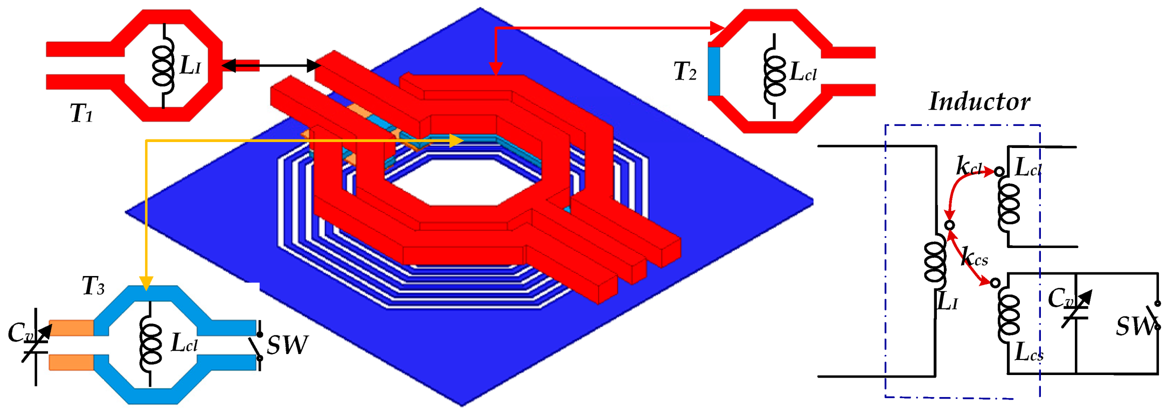
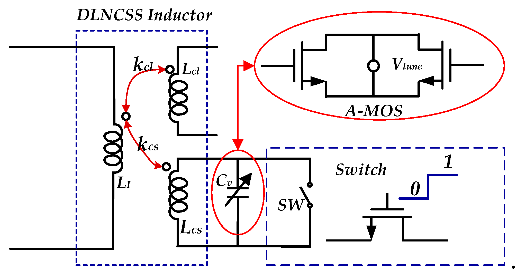
A DLNCSS inductor was presented to realize the performance balance of the phase noise and tuning range in a D-band VCO design in this paper. The DLNCSS inductor is shown in
Figure 2. This inductor is based on a triple-coupling winding transformer. The coil
T1 is used as the inductor in the LC tank of VCO. The edge-coupling coil
T2 transfers the oscillator signal to the output buffer. The varactor and switch are located at the vertical-coupling coil
T3 of this triple-coupling winding transformer. Therefore, the magnetic coupling coefficient between the coil
T1 and coil
T3 varies when the value of the varactor changes or the switch turns on and off. As a result, the value of the inductor (coil
T1) changes for improving the FTR of VCO. A PGS is used for this DLNCSS inductor, preventing the capacitive coupling to the substrate and reducing the coupling of noise from the substrate. Meanwhile, the
Q of this DLNCSS inductor is improved.
As discussed in [
16], the inductor with a PGS can be treated as a transformer while using an equivalent circuit model. Based on this analysis and conclusion, a simple equivalent circuit model of the DLNCSS inductor was proposed for the designing of the inductor in this paper, as shown in
Figure 3. The coupling effects between coil
T2 and the coil
T3 are not taken into account for the easy analysis here.
As shown in
Figure 3, the input impedance
Zin can be expressed in Equation (4)
where
LI and RI represent theself-inductance and metal series resistance of the coil
T1 of the designedDLNCSS inductor.
Zp,
Zcs, and
Zcl denote the reflected impedance of the PGS and the different coupling coils
T2 and
T3, respectively.
The reflected impedance
Zp is expressed as
where
Mp is the mutual inductance, and
kp is the effective magnetic coupling factor.
Rp and
Lp denote the resistance and the corresponding inductance of the PGS, and
LI is the self-inductance of the coil
T1 of the designed DLNCSS inductor.
The reflected impedance
Zcs is expressed as
where
Mcl is the mutual inductance, and
kcl is the effective magnetic coupling factor.
Lcl represents the corresponding inductance of the self-inductance of the coil
T2 of the designed DLNCSS inductor.
Ccland
Rcl represent the load of the coil
T2.
The reflected impedance
Zcs is expressed, as shown in Equations (7a) and (7b) when the switch turns on and off.
where
Mcs is the mutual inductance, and
kcs is the effective magnetic coupling factor.
Lcs represents the corresponding inductance of the self-inductance of the coil
T3 of the designed DLNCSS inductor. The varactor named
Cv is used for tuning the frequency of VCO.
Ron represents the resistance when the switch turns on.
Rof f and
Coff denote the equivalent capacitance and the equivalent resistance when the switch turns off.
The working frequency of the proposed VCO in this paper was above 100 GHz, and the parasitic resistance of
Rp,
Rcl, and
Rcs was only about a few ohms.
,
and
are approximate to zero. Therefore, we could draw that the effective inductance (
Len) and the effective resistance (
Ren) of the DLNCSS inductor can be expressed in Equations (8a) and (8b) when the switch turns on.
The effective inductance (
Lef) and the effective resistance (
Ref) of the DLNCSS inductor can be expressed in Equations (9a) and (9b) when the switch turns off.
From the Equations (8a) and (8b) and Equations (9a) and (9b), we could draw that the effective inductance changes when the switch turns on and off or the value of the varactor varies. The effective resistance increases while the switch turns on and off. As a result, the quality factor (
Qeff) of the DLNCSS inductor decreases. The
Qeff is expressed as
2.3. Design of DLNCSS Inductor
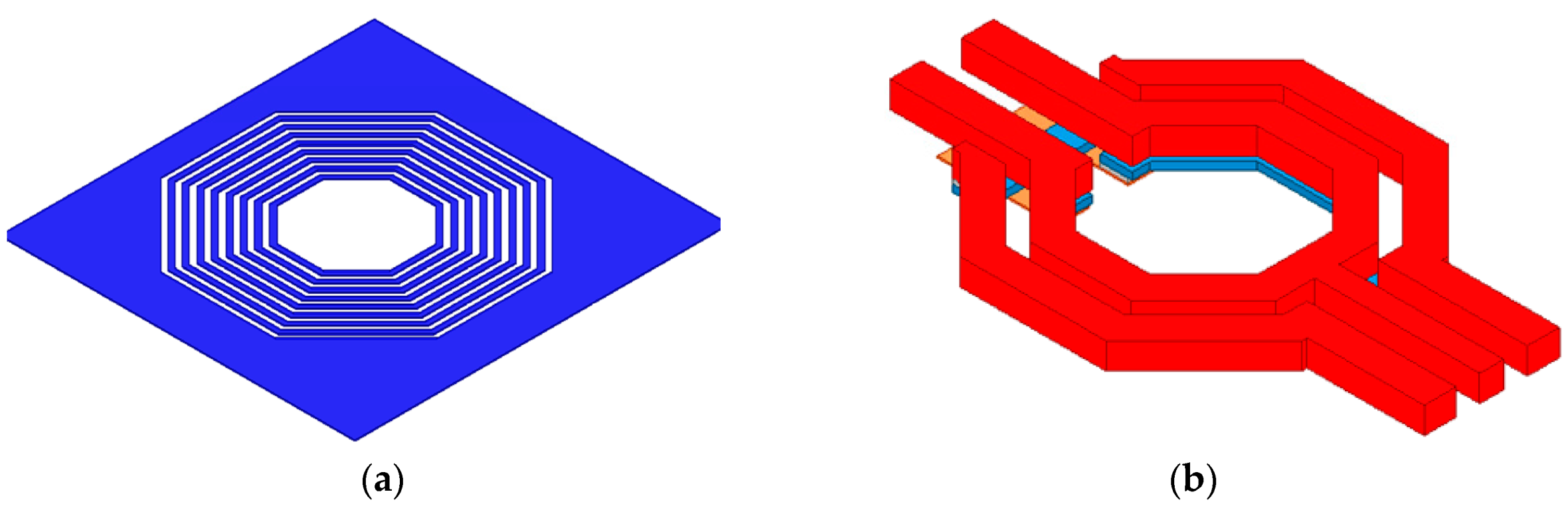
Based on the discussion of the substrate loss, the PGS of the inductor, and the proposed DLNCSS inductor, the inductor in a 65 nm CMOS process was carefully designed and optimized with the aid of the EM simulation in this paper.
The structure of the DLNCSS inductor is shown in
Figure 2. As discussed in Equation (8b) and Equation (9b), we found that the resistance of the secondary coil (
T2 and
T3) also contributes to the effective resistance (
Reo and
Ref). As a result, the
Qeff reduces, and the phase noise of VCO deteriorates. Thus, the top metal
M8(with the thickness of 3.3 μm) and second top metal
M7 (with the thickness of 0.9 μm) are used to design this DLNCSS inductor because the resistivity of these two top metal is lower than that of the other metals in the process. In this way, the metal series resistance of the DLNCSS inductor decreases, and the
Q of this inductor improves. The top metal
M8is adopted to design the coil
T1 used as the inductor and the coil
T2 that is used to coupling the generated signal of VCO to the output buffer. Thus, the coupling capacitor used between the cross-pair and the output buffer could be omitted. Meanwhile, the design deviation of VCO could also be alleviated, which is introduced by the capacitor supplied by the foundry. The coil
T3 connecting the varactor and switch is designed by using the second top metal
M7.
It is well known that the resistance could be reduced when the line width of the coil of the DLNCSS inductor increases, but the parasitic capacitance of the coil increases as the line width of the coil widens. This will cause the SRF of the DLNCSS inductor to reduce. The VCO works near the SRF of the DLNCSS inductor and will deteriorate the performance of VCO, or even fail it. After careful design, the width of the coil (T1, T2, and T3) was selected to be 4 μm as a compromise in this work.
As discussed in
Section 2.1 of this paper, the substrate loss leads to a reduction of the
Q of the inductor. The PGS could improve this situation, but it also leads to the reduction of the
Q as the resistance of the PGS cannot be neglected in the mm-wave frequency band. A PGS is also used for the presented DLNCS-T inductor to improve this
Qeff, which is shown in
Figure 4a. It is used as the ground shield for an inductor reported in [
20]. This PGS comprises the ring metal strips and the irregular metal pattern. According to the discussion in [
20], the induced current flowing in the ring metal strips is generated by the variation of the electromagnetic field of the inductor. This induced current generates the electromagnetic field in the different ring metal strips. The variation of the electromagnetic field in those ring metal strips could weaken the electromagnetic field between each other. Thus, the negative coupling between the inductor and the PGS reduces, and the
Q of the proposed DLNCSS inductor improves. The PGS used in this paper is designed by using the bottom metal
M1, and the width of the ring metal strips is 1 μm, and the space between different ring metal strips is 1 μm.
The inductance
L of the proposed DLNCSS inductor could be evaluated by using Equation (11).
Thus, the curves of the inductance of the proposed DLNCSS inductor are shown in
Figure 5a when the switch turns on and off. As shown in
Figure 5a, the SRF of the presented DLNCSS inductor doesn’t appear in the range from 75 GHz to 200 GHz. Therefore, this DLNCSS inductor was suitable for the design of VCO in this paper. Due to the effects of the parasitic capacitance of the MOS switch and the lack of subtly design considerations, the inductance difference between
Ls and
Lo is not so great when the switch turns on and off. As a result, the tuning frequency range of VCO decreased in this work. The simulation and the measurement results of the presented VCO have also shown this phenomenon of the small tuning range in
Section 4.
Figure 5b shows the curve of
Q of the DLNCSS inductor and the switch inductor loaded transformer without PGS. This switch inductor loaded transformer without PGS is shown in
Figure 4b, which is employed to compare with the DLNCSS inductor and show the improvement of Q while using the PGS for the switch inductor loaded transformer. It is found that the
Q increases while the frequency increases from DC to 190 GHz. The value of
Q of the DLNCSS inductor is larger than 10 in the whole D-band frequency. The
Qs and
Qo of the DLNCSS inductor are with the same value when the switch turns on and off, and the
Q isn’t affected by the on and off state of the switch. Because the PGS is used for the proposed DLNCSS inductor, the
Q of the DLNCSS inductor is larger than that of the switch inductor loaded transformer without PGS. The value of
Qref of the inductor shown in
Figure 4b is less than 8 in the whole D-band frequency range. As a result, it is drawn from Equation (1) that the phase noise of the VCO is improved while using the proposed DLNCSS inductor.
3. Design and Discussion of the Proposed VCO
A D-band VCO was designed by using the proposed DLNCSS inductor in this paper, and the schematic is shown in
Figure 6. This presented D-band VCO consisted of the negative resistance cell named
-R cell, a transformer-coupled resonant tank, comprising of DLNCSS inductor, MOS switch, differential common-cathode varactor, an output buffer, and the matching networks. The negative resistance cell adopted the cross-couple pair with a tail current source, which is shown in
Figure 6. The cross-couple pair was realized by using the transistors named
M1 and
M2. The output buffer shown in
Figure 6 employed a differential cascode amplifier to fulfill high isolation between the negative resistance cell and the load of the VCO, such as power amplifier, divider, and so on. The transistors named
M5 and
M6 were the input device of this buffer, and the transistors named
M3 and
M4 were the cascode devices of this buffer. The output matching networks adopted the transmission line
Lm and a transformer to achieve the impedance matching of 50 ohms.
3.1. Active Circuits Design Details
The negative resistance cell and the output buffer were the active parts of the VCO presented in this paper. Their quality would directly affect the performance of the VCO, such as start-up and stable oscillation, output power, phase noise, and so on.
The negative resistance cell was used to compensate for the loss from the LC tank and sustain the oscillation of the VCO, which was a function of the transconductance of the MOSFET at the frequency of the oscillation. The parasitic capacitance of the MOSFET (Cgd, Cgs) and the parasitic of the gated routing reduced the effective transconductance of the negative resistance cell. Meanwhile, the effective transconductance degraded as the operating frequency increased.
The effective transconductance could be improved by increasing the size of the MOSFET or the current of the negative resistance. A large size MOSFET, however, suffered from the large parasitic capacitance. These parasitic capacitances degraded ft and fmax of the MOSFET. Meanwhile, the performance of VCO was also reduced, such as the tuning range, phase noise, operating frequency, and so on.
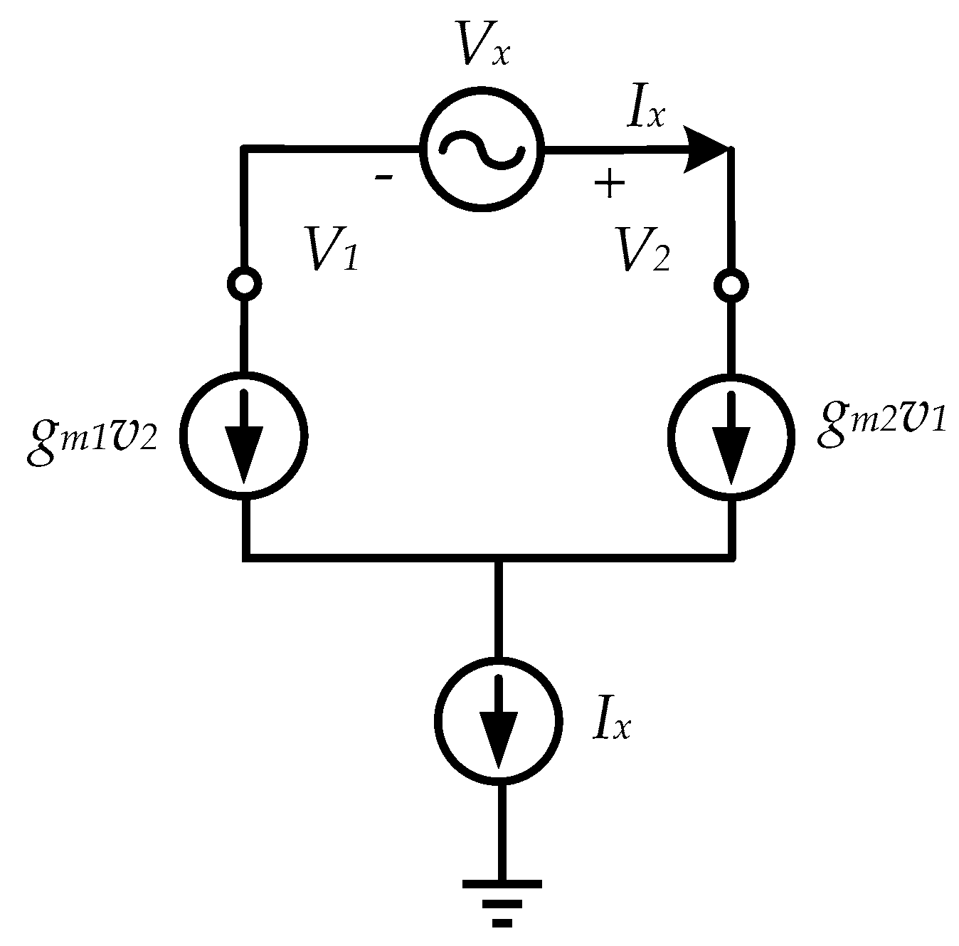
Although the VCO worked under large signal characteristics, it was always analyzed by using a small signal model for the convenient analysis of VCO.
Figure 7 shows the small signal model of the negative resistance cell used for the analysis of the cross-couple pair in this work.
Since the transistors used in the cross-couple pair had the same size, the negative resistance
Rngc was deduced and expressed as,
After careful design, the value of the
gm introduced by the cross-coupled pair was slightly higher than the conductance introduced by the LC tank for the VCO design in this paper. A tail current source device named
Mq was employed to alleviate the effects of the input common-mode level variations on the operation of the cross-couple pair transistor (
M1 and
M2). Meanwhile, the current of the negative resistance cell could be changed by adjusting the bias voltage of this tail current source. Thus, the VCO could start-up even though the situation of PVT (Process, Voltage and Temperature) changed. Finally, the width of the
M1 and
M2 were selected as 1
μm when the length was 60 nm, and the width of the
Mq was selected 2 μm when the length was 60 nm. To obtain the maximum with 65-nm nMOS transistors, the individual finger width of the nMOS transistor of the cross-coupled pair was designed to be 1 μm [
21], and the total finger number was designed to be 24 to provide sufficient negative resistance. The gate routing was also optimized to reduce the parasitic resistance in this design. The layout route and the parasitic resistance were given careful consideration, and at the same time, the metal
M5 and metal
M6 were selected, and their width was 0.5 μm.
The output buffer was designed to drive the load of the measuring instrument, which helped to evaluate the performance of the VCO designed in this paper. The load impedance of the VCO could be transferred to the cross-couple pair if the isolation of the output buffer was small. This would cause the VCO to stop working in the worst case. As a result, the size of the cross-couple transistors needs to be increased to compensate for the transferred load impedance, resulting in a decrease in oscillate frequency, especially in the mm-wave frequency band. There were usually 2 kinds of buffers, one was the common source (CS) amplifier, and the other was the cascode amplifier. They are shown in
Figure 8a and
Figure 8b, respectively.
The isolation between the negative impedance cell and the load could be evaluated by the output resistance of these two kinds of buffers. The output impedance of the CS amplifier and the cascode amplifier is expressed in Equation (13) and Equation (14), respectively.
where
is the transconductance of the M
7.
where
CX represents the equivalent capacitance that is seen from node
X in
Figure 8b.
is the transconductance of the
M9.
It was drawn that the output impedance of the CS amplifier was capacitive, and the output impedance of the cascode amplifier had the capacitive impedance and the resistor. Thus, the cascode amplifier had better isolation than the CS amplifier. The cascode amplifier was adopted to design the output buffer for VCO design in this paper. The schematic is shown in
Figure 6. After carefully designing, the width of the
M5 and
M6 was 6.4 μm, and the width of the
M3 and
M4 was 12 μm, while the length of those MOSFETs was 60 nm. The isolation of the designed output buffer was less than −35 dB.
3.2. Transformer-Coupled Resonant Tank and Output Matching Networks
It was drawn from Equation (1) that the loss of the LC-tank affected the phase noise of the VCO. Therefore, the Q of the LC-tank was improved in many ways in this paper. Besides, the PGS was designed to reduce the substrate loss, and the top-metal was used and optimized to reduce the ohmic loss of the metal; the transformer-coupled resonant tank was also used to improve the Q of the LC-tank in this paper.
There were usually two ways to connect the differential varactor in the design of VCO, one was a common-anode structure, and the other one was the common-cathode structure. The common-anode structure had a lower
Q than that of the common-cathode structure. The anode of the varactor needed to be connected to the ground via a resistor while using the common-cathode structure. As a result, the phase noise increased. A transformer-coupled resonant tank was proposed and discussed in [
9], which helped to improve the
Q of the LC-tank. An improved transformer-coupled resonant tank was proposed to improve the
Q of the LC-tank in this paper, which consisted of DLNCSS inductor and the differential varactor with common-cathode structure. The simple equivalent circuits of this improved transformer-coupled resonant tank are shown in
Figure 9.
Unlike in [
9], this improved transformer-coupled resonant tank presented in this paper was based on a triple-coil transformer, and the differential varactor employed common-cathode structure and MOS switch were connected to the secondary coil of this triple-coil transformer. Thus, the phase noise of the VCO and the tuning range were improved at the same time. A-MOS varactor was used in this design because it is less vulnerable to latch-up and has a compact geometry and relatively high-quality factor.
The output buffer was designed to evaluate the performance of VCO. It was important to design proper matching networks between the buffer and the load of the measuring instruments. Considering the passive devices offered by the Foundry was a scalable model at the D-band frequency, and it was not a completely accurate model. The performance of the VCO would degrade if those passive devices were used in the design. Thus, the on-chip transmission line (T-line) and the on-chip transformer were used to fulfill the matching between the buffer and the load of 50 ohms. These T-line and the transformer were evaluated by the EM simulation [ADS (Advanced Design System) momentum]. The transformer was used here to fulfill the impedance matching and the transition from the differential to the single-end. The incompletely accurate model in D-band and the EM simulation deviation would lead to an oscillating frequency shift of the VCO. Therefore, a wide-band matching network was designed to ensure the output signal could be detected by the testing instruments. The T-line was employed for the matching networks to realize the wide-band matching networks as the degree of the freedom of the matching networks increased after using the T-line. The matching network is shown in
Figure 10. T-line and the edge-coupling transformer were designed by adopting the top and thick metal to reduce the metal loss of the matching networks. After careful design and optimization, the width of the T-line and the edge-coupling transformer was 3 μm. The lower metal M1was designed as a shield ground of T-line and the transformer, which was adopted to prevent electromagnetic (EM) fields from the lossy silicon substrate and improve the loss of the matching networks.
4. Fabrication, Measurement, and Discussion
This presented VCO was fabricated with the use of the DLNCSS inductor in a 65 nm CMOS process, that is, with a cut-off frequency of 210 GHz. All of the on-chip passive elements designed in this paper were a shield from the lossy substrate by using the bottom metal M1 in the process. This ground shield could prevent the capacitive coupling to the substrate, reducing the coupling of noise from the substrate to the passive elements. Then, the
Q of those passive elements was improved. Therefore, the phase noise of VCO was improved. At the same time, all the passive elements were designed and evaluated by using the ADS momentum before the fabrication. The microphotograph of the proposed VCO is shown in
Figure 11. The size of this VCO was 0.23 mm
2, including all RF pads and DC pads. Many DC-PADs were located in the layout of VCO to offer the DC power, DC ground, and other control voltage source, which was used for the measurement of proposed VCO. As a result, the size of the VCO, including all PADs, was large, and lots of metal dummy were used in the layout. This VCO consumed a DC power of 11.2 mW with a supply voltage of 1.4 V.
Figure 12 shows the measurement setup for the proposed VCO. The DUT (device under test) was placed on the probe station. DC supply of the VCO was loaded by using an external voltage source. The single-ended output of the DUT of the VCO proposed in this paper was connected to the D-band GSG (Ground-Signal-Ground) probe with the loss of 2 dB, then to the harmonic mixer module with the loss of 2.5 dB, and finally to the spectrum analyzer. Thus, the output signal of the VCO designed in this paper could be detected by the spectrum analyzer. There was a 4.5 dB attenuation of the output signal that flows through the waveguide and probe.
Figure 13 shows the output spectrum of the proposed VCO when the DC supply voltage was 1.4 V and the bias voltage of the transistor named
Mq, in
Figure 6, was 0.7 V. The output power was −10.9 dBm while considering the 4.5 dB loss of the measuring instrument. This 4.5 dB loss comprised of 2 dB loss introduced from the GSG probe and 2.5 dB loss introduced from the waveguide.
The oscillation frequency and output power versus tuning voltage are shown in
Figure 14. The simulated and the measured results are also shown in the same figure in
Figure 14 to help to compare the results easily.
Figure 14a shows the operating frequency and the output power of the presented VCO when the switch was on, and
Figure 14b shows operating frequency and the output power of the VCO when the switch was off. As shown in
Figure 14, the measured operating frequency ranged from 128.76 GHz to 129.56 GHz. In this frequency band, the output power ranged from −11.8 dBm to −10.6dBm. The simulated working frequency of the VCO ranged from 139.2 GHz to 140.1 GHz when the switch was off, and it ranged from 139.6 GHz to 140.45 GHz when the switch was on. The simulation results showed that the output power ranged from −8.3 dBm to −7.7dBm, and the tuning range was of 1.25 GHz. The simulated oscillation frequency showed that there was an overlap frequency range of 0.5 GHz when the switch turned on and off. The major cause of this phenomenon was the small inductance difference between the on-state and off-state of the presented DLNCSS inductor. Meanwhile, this small inductance difference led to a reduction of the tuning range of approximately 0.5 GHz.
Comparisons with the simulated results, the operating frequency dropped by 7.7%. The whole frequency tuning range of this VCO was 0.8 GHz, which degraded to 0.45 GHz, while the simulated tuning range was 1.25 GHz. There were two main reasons for those deviations. One was mainly due to parasitic capacitances introduced by random dummy metal filling, which was not fully taken into account in the EM simulation. The other one was the imprecise transistor model in D-band frequency.
The phase noise was evaluated at 1 MHz off the carrier in 1 Hz bandwidth. For the shortage of the measurements,
Figure 15 shows the simulated phase noise of the proposed VCO. The phase noise was observed when the operating frequency was adjusted equal to the measurement value. The phase noise at a 1 MHz offset from the carrier frequency was less than −82 dBc/Hz in the whole working frequency range from 128.76 GHz to 129.56 GHz.
Table 1 summarizes the performance of the presented VCO and the other state-of-the-art works. Compared with other works, this VCO had better RF-to-DC efficiency than that in [
1,
4,
5]. Meanwhile, the FOM (Figure of Merit) of the presented VCO was better than that in [
4].
Note that the FOM of the oscillator was expressed as
where
is the phase noise at the offset frequency,
is the oscillation frequency, and
is the DC power consumption in mW.

 ,
, 


