Article

A Reconfigurable CMOS Inverter-based Stacked Power Amplifier with Antenna Impedance Mismatch Compensation for Low Power Short-Range Wireless Communications

Division of Electronic Engineering, Jeonbuk National University, Jollabuk-do 561-756, Korea
*
Authors to whom correspondence should be addressed.
Electronics 2020, 9(4), 562; https://doi.org/10.3390/electronics9040562
Submission received: 17 February 2020 / Revised: 19 March 2020 / Accepted: 25 March 2020 / Published: 27 March 2020
(This article belongs to the Special Issue CMOS Power Amplifier Design and Applications)

Abstract

:
A reconfigurable CMOS inverter-based stacked power amplifier (PA) is proposed to extend impedance coverage, while maintaining an output power exceeding the specific power level under the worst antenna impedance mismatch conditions. The adopted process technology supports multi-threshold metal-oxide-semiconductor field-effect transistor (MOSFET) devices, and therefore, the proposed PA employs high threshold voltage (Vth) MOSFETs to increase the output voltage swing, and the output power under a given load condition. The unit cell of the last PA stage relies on a cascode inverter that is implemented by adding cascode transistors to the traditional inverter amplifier. By stacking two identical cascode inverters, and enabling one or both of them through digital switch control, the proposed PA can control the maximum output voltage swing and change the optimum load Ropt, resulting in maximum output power with peak power added efficiency (PAE). The cascode transistors mitigate breakdown issues when the upper cascode inverter stage is driven by a supply voltage of 2 × VDD, and decrease the output impedance of the PA by changing its operation mode from the saturation region to the linear region. This variable output impedance characteristic is useful in extending the impedance coverage of the proposed PA. The reconfigurable PA supports three operation modes: cascode inverter configuration (CIC), double-stacked cascode inverter configuration (DSCIC) and double-stacked inverter configuration (DSIC). These show Ropt of around 100, 50 and 25 Ω, respectively. In the simulation results, the proposed PA operating under the three configurations showed a saturated output power (Psat) of +6.1 dBm and a peak PAE of 41.1% under a 100 Ω load impedance condition, a Psat of +4.5 dBm and a peak PAE of 44.3% under a 50 Ω load impedance condition, and a Psat of +5.2 dBm and a peak PAE of 37.1% under a 25 Ω load impedance condition, respectively. Compared to conventional inverter-based PAs, the proposed design significantly extends impedance coverage, while maintaining an output power exceeding the specific power level, without sacrificing power efficiency using only hardware reconfiguration.

1. Introduction

As wireless electronic devices continue to be miniaturized, and further support multi-functionality, antenna size reduction is required because most mobile platforms have a limited space for all of the necessary antennas. The small radiator size of a miniaturized antenna greatly reduces its bandwidth, and this leads to a high quality factor (Q-factor) for the antenna.
As a result, the antenna impedance becomes more sensitive to environmental changes, leading to several important considerations and challenges in designing RF front-end circuits, such as low noise amplifiers (LNAs), power amplifiers (PAs) and RF switches. One major concern is the preservation of the peak output power and power-added efficiency (PAE) of a PA in the worst antenna impedance mismatch conditions. Because most PAs are designed to drive a standard 50 Ω impedance load using a dedicated output matching network, antenna impedance mismatch significantly affects peak output power and PAE performance. For instance, it was reported by Keerti et al. that the output power of a PA decreases as much as 5 dB for a load mismatch with a voltage standing-wave ratio (VSWR) of 10:1 [1].
The most common method used to compensate for antenna impedance mismatch, and to preserve the RF performance of a PA, is to use a tunable matching network (TMN) between the PA and the antenna [2,3,4]. To adapt to changes in antenna impedance, the TMN adjusts its impedance to match the overall impedance of the TMN and antenna to 50 Ω. In implementing the TMN, it is very important to build high Q-factor passive devices (inductors and capacitors) with good linearity in order to minimize power loss and avoid signal distortion. In addition, to compensate the antenna impedance mismatch over a wide range of the Smith Chart, it is better to increase the tuning range of the integrated tunable capacitor, while keeping a high Q-factor and good linearity. Unfortunately, on-chip spiral inductors fabricated on silicon substrates suffer from poor Q-factors, and the use of off-chip inductors with high Q-factors is not desirable, because of cost and limited printed circuit board (PCB) size. Regarding integrated tunable capacitors in CMOS, the most common topology of the digitally controlled switched capacitor array inevitably faces a fundamental trade-off between the Q-factor and the tuning range [5], and its performance degrades as the operating frequency increases. Some emerging technologies, such as micro-electro-mechanical systems (MEMS) and barium strontium titanate (BST), have been proposed for use in the implementation of low-loss, wide-tuning-range tunable capacitors [6,7]. However, these technologies require a high tuning/switching voltage (>30 V), which of course is unsuitable in battery-driven mobile handsets. Additionally, they have not been proven in high-volume production.
In this paper, a reconfigurable CMOS inverter-based stacked PA for 2.4 GHz low power short-range wireless communications is designed to maintain nearly constant output power in the presence of antenna impedance variation. Through only hardware reconfiguration, and without a TMN, impedance coverage was significantly extended compared to the conventional inverter-based PAs, maintaining an output power exceeding the specific power level without sacrificing power efficiency.

2. Circuit Design

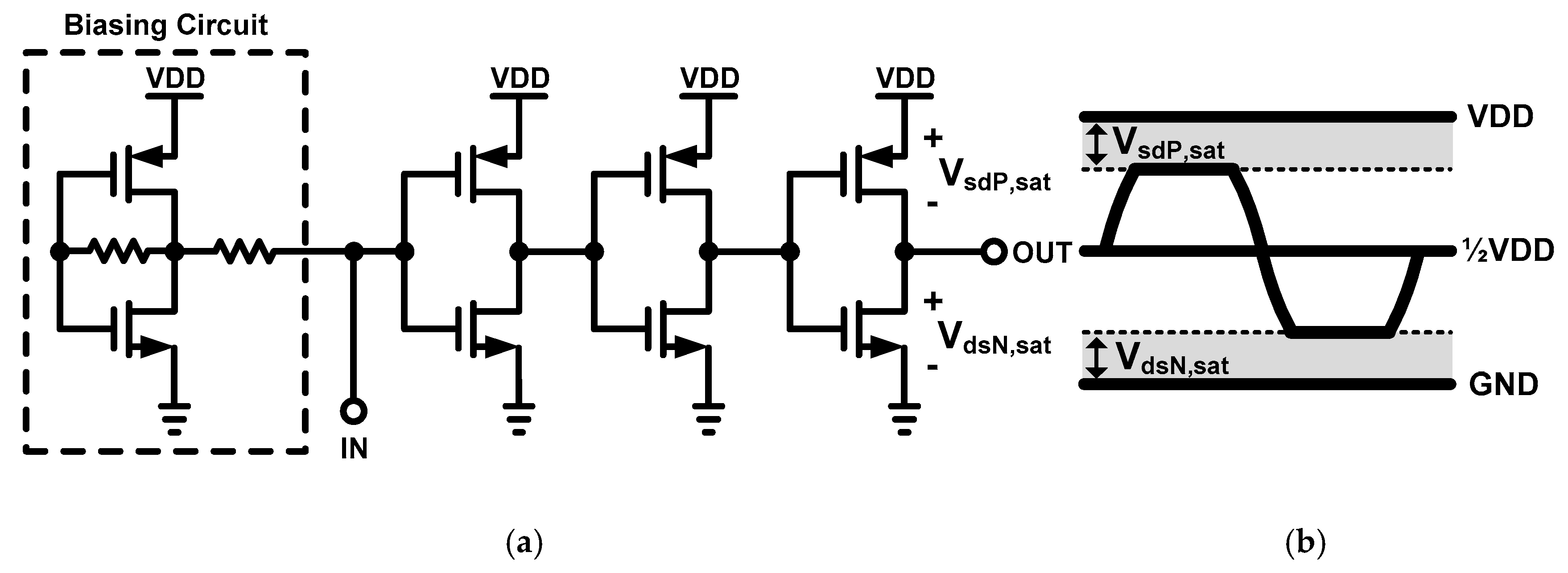
2.1. Conventional Inverter-based PA

All modern RF transceivers for low power short-range wireless communication technologies, such as Bluetooth Low Energy (BLE), IEEE802.15.4 (ZigBee), Z-wave, Thread and IEEE802.15.6 (Medical Body-Area Networks, MBAN), are integrated with highly reconfigurable digital baseband modems to provide single-chip solutions, and keep costs down [8,9,10]. By making use of the technology scaling available with the deep-submicron CMOS process, single chip integration of RF/analog circuits and digital circuits with micro-processor cores on a common CMOS system-on-chip (SoC) platform has become a development trend, and provides the critical advantages of low cost and low power consumption. However, with this approach, the design of traditional RF/analog circuits is difficult. Furthermore, some special masks needed to implement metal–insulator–metal (MIM) capacitors and thick metal layers are not acceptable from a fabrication cost standpoint. To compensate for the increasing mask costs of scaled CMOS technologies, RF circuitry, including PAs, should be fabricated on a small silicon area, and be compatible with a standard, low cost digital CMOS process, where there is no burden on the back-end-of-line (BEOL), resulting from the stringent Q-factor requirements of on-chip inductors (or transformers). In addition, it is better to design digital-intensive and digital-oriented RF/analog circuits to exploit many advantages of technology scaling. For these reasons, inverter-based PAs have been widely adopted for low power short-range wireless technologies.
Figure 1a shows a schematic of a conventional three-stage inverter-based PA. The hardware configuration is very simple, because there are no inductors or transformers, and as a result, it is easily implemented in a low cost digital CMOS process The previous works of Paidimarri et al. [11], Kiumarsi et al. [12], and Van Langevelde et al. [13] presented the inverter-based, push-pull topologies for PA applications, but there was no study for compensating the antenna impedance mismatch effect with the same RF performances. The first and second stages are drive amplifiers (DAs) for boosting the weak input signal with sufficiently high gain and extremely low power consumption, and the last stage is the output stage for obtaining maximum output power under the given load condition. Instead of using a dc biasing method with a shunt feedback configuration, a replica biasing circuit is adopted to provide a stable dc operating point to the inverter stage, and to ensure a rail-to-rail output swing. By adjusting the channel width ratio between the NMOS and PMOS transistors, the dc operating point of the inverter stages is around half of VDD. Compared to a common-source topology with an inductor load, the output voltage swing of the inverter-based PA is reduced by almost half. As shown in Figure 1b, its output voltage swing is expressed as
V d s N , s a t v o u t V D D V s d P , s a t
( V g s , N | V t h , N | ) v o u t V D D ( V s g , P | V t h , P | )
where Vgs,N and Vsg,P are the gate-to-source and source-to-gate dc bias voltages applied to the NMOS and PMOS transistors, and Vth,N and Vth,P are the threshold voltages of the NMOS and PMOS transistors. Typically, Vgs,N and Vsg,P are set to be equal to half of VDD to maximize the output voltage swing. From (1) and (2), it can be seen that it is desirable to increase the threshold voltage (Vth) of the MOSFET for the maximum output voltage swing. Modern deep-submicron CMOS technologies support multiple-Vth MOSFETs to reduce leakage power by assigning a high Vth to some transistors in non-critical paths. Therefore, for a simple hardware configuration, in the circuit design for the last stage of the inverter-based PA, high-Vth MOSFETs are used instead of applying a body bias voltage to increase Vth in regular-Vth MOSFETs. Figure 2 shows the simulated output power, the PAE and the power contour of the three-stage inverter-based PA using regular-Vth MOSFETs and high-Vth MOSFETs under a 50 Ω load impedance condition. Both PAs were designed to consume the same static dc current of 2.3 mA. The saturated output power (Psat) and peak PAE are +1.2 dBm and 32.6% for the PA with the regular-Vth MOSFETs and +2.8 dBm and 41.4% for the PA with the high-Vth MOSFETs. As predicted, using the high-Vth MOSFETs increases the output voltage swing without any additional dc current, enhances Psat and peak PAE, and extends the impedance coverage while maintaining an output power of greater than 0 dBm.

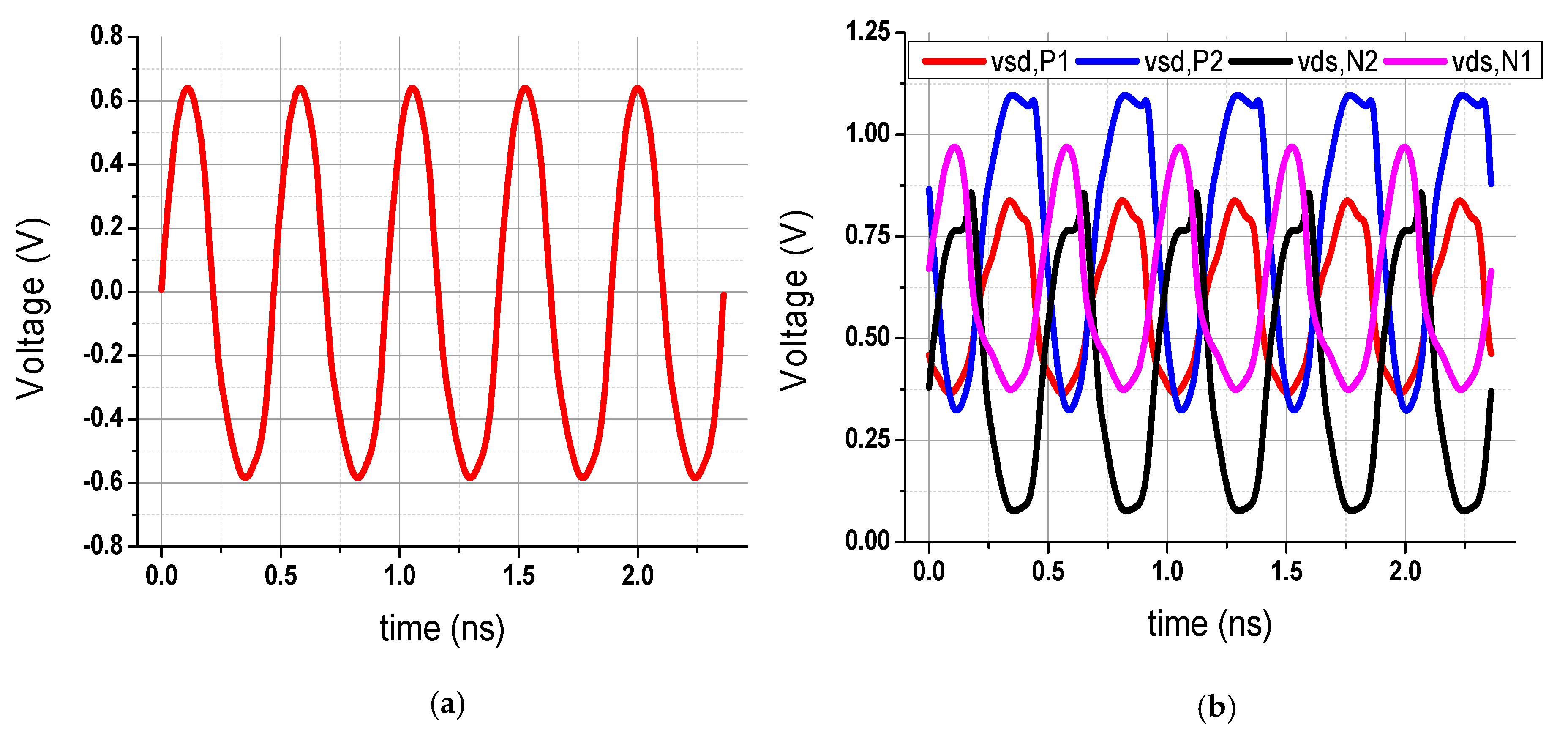
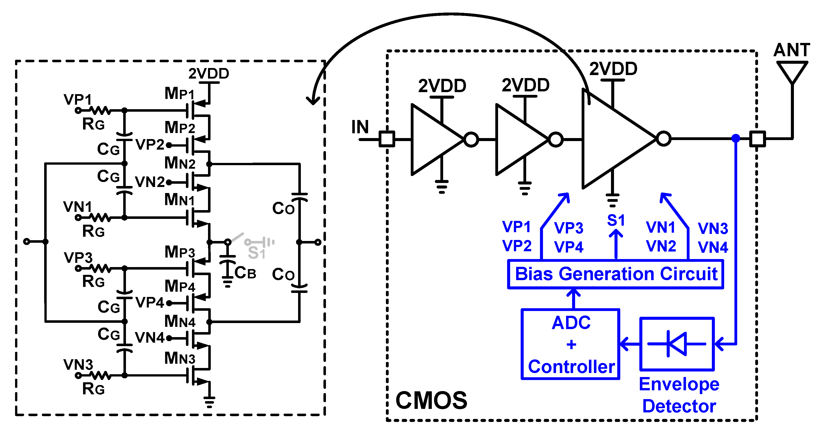
2.2. Proposed Reconfigurable Cascode Inverter-based Stacked PA

The most efficient output power (Pout,eff) of a PA is determined by the optimum load impedance Ropt and maximum (zero-to-peak) output voltage swing vout,max. This relationship is given as
P o u t , e f f v 2 o u t , m a x 2 R o p t .
Equation (3) implies that the PA can extend the impedance coverage while maintaining an output power exceeding the specific power level by varying vout,max through hardware reconfiguration. Figure 3 shows the proposed reconfigurable cascode inverter-based stacked PA driven by a supply voltage of 2 × VDD with three operation modes. The first and second stages are DA stages, while the last stage is a PA stage. In designing the DA, to alleviate the breakdown issues resulting from operating at a supply voltage of 2 × VDD, two identical inverters are stacked in series, and a bypass capacitor is placed between them to short ac signals to ground at the operating frequency. For all stages, high-Vth MOSFETs are employed to enhance Psat and peak PAE. All transistors in the proposed reconfigurable PA are thin gate oxide MOSFETs for high frequency operation. The unit cell of the last PA stage is based on a cascode inverter, which is implemented by adding cascode transistors (MN2 and MP2) to the traditional inverter amplifier (MN1 and MP1). The cascode transistors mitigate breakdown issues when the upper cascode inverter stage is driven by a supply voltage of 2 × VDD alone, and also decrease the output impedance of the PA by changing its operation mode from the saturation region to the linear region. This variable output impedance characteristic is useful in extending the impedance coverage of the reconfigurable PA. By stacking two identical cascode inverters, and enabling one or both of them through digital switch control, the proposed PA can control the value of vout,max in (3), and eventually change Ropt, yielding the maximum output power with peak PAE. The resistance value of RG (10 kΩ) is high enough to block ac signals, and only pass dc bias voltage. The capacitance value of CG, CO and CB are 2 pF, 10 pF and 10 pF, respectively, in this design. Similarly, their capacitance value is high enough to block dc bias voltage and only pass ac signals. It was verified through simulation that their side effects on the overall performance were negligible.
In the cascode inverter configuration (on the far left in Figure 3), the middle spot between the two cascode inverters is directly connected to the physical ground through switch S1, and the upper cascode inverter, which is composed of transistors MN1, MN2, MP1 and MP2 operated in the saturation region, is only enabled. The output voltage swing in this mode is given as
V d s N 1 , s a t + V d s N 2 , s a t v o u t 2 V D D V s d P 1 , s a t V s d P 2 , s a t
( V g s , N 1 | V t h , N 1 | ) + ( V g s , N 2 | V t h , N 2 | ) v o u t 2 V D D ( V s g , P 1 | V t h , P 1 | ) ( V s g , P 2 | V t h , P 2 | )
where Vgs,N1(2) and Vsg,P1(2) are the gate-to-source and source-to-gate dc bias voltages applied to MN1(MN2) and MP1(MP2), and Vth,N1(2) and Vth,P1(2) are the threshold voltages of MN1(MN2) and MP1(MP2). Assuming the overdrive voltage VdsN1,sat, VdsN2,sat, VsdP1,sat and VsdP2,sat are all 0.2 V, the nominal supply voltage VDD is 1.2 V, and a maximum output power of around +6 dBm is delivered to the load by the PA. The value of vout,max and Ropt are calculated to be 0.8 Vop and 80 Ω using Equation (3). Figure 4 shows the load-pull simulation results of the proposed reconfigurable PA for the three modes. The simulated Ropt yielding a maximum output power of around +6 dBm is about 100 Ω for the cascode inverter configuration. This closely matches the calculated result. Because the upper cascode inverter is driven by a supply voltage of 2 × VDD (greater than the nominal supply voltage VDD), it is important to ensure in the design that the transistor’s drain-to-source voltage swing does not exceed the pre-specified value of its drain-to-source breakdown voltage (BVDS). This prevents the permanent damage and gradual degradation in device performance over time caused by gate-oxide breakdown and hot carrier degradation. Figure 5 presents the simulated output voltage waveform, source-to-drain voltage waveforms driven by MP1 and MP2 (vsd,P1 and vsd,P2), and drain-to-source voltage waveforms driven by MN2 and MN1 (vds,N2 and vds,N1) when the proposed PA in the cascode inverter configuration generates an output power of +3 dBm under a 100 Ω load impedance.
It can be seen that the cascode transistors MP2 and MN2 share the burden of the over-voltage stress and mitigate the breakdown issues of the thin gate oxide MOSFETs. Because all source-to-drain and drain-to-source voltage swings do not exceed the BVDS of 1.2 V provided by the adopted process technology, and because this is ac stress instead of dc stress, the cascode inverter configuration of the proposed PA does not experience device breakdown.
In the double-stacked cascode inverter configuration, both the upper and lower cascode inverters are enabled. Switch S1 is open, the middle spot between the two cascode inverters is biased at half of the 2 × VDD supply voltage, and this node is ac grounded through the large bypass capacitor CB. Ideally, this should yield almost the same maximum output power as the aforementioned cascode inverter configuration because the total output current is doubled by combining the two output currents from the upper and lower cascode inverters, while the final output voltage swing is reduced by half. This implies that the value of Ropt, which yields the maximum output power from the double-stacked cascode inverter configuration, is lower than that of the cascode inverter configuration. As shown in Figure 4a,b, the double-stacked cascode inverter configuration provides a simulated Ropt of around 50 Ω, which is approximately half the value of the simulated Ropt of the cascode inverter configuration. Unfortunately, because the two output currents generated from the upper and lower cascode inverters are not completely identical due to mismatches, a slight degradation (1–2 dB) of the maximum output power is unavoidable.
The last mode of the proposed reconfigurable PA is the double-stacked inverter configuration of the circuit schematic on the far right in Figure 3. Unlike in the double-stacked cascode inverter configuration, all cascode transistors MP2, MP4, MN2 and MN4 operate in the linear region as switches by applying a gate-to-source (source-to-gate) voltage of VDD to the NMOS (PMOS) transistors MN2 and MN4 (MP2 and MP4), and completely turning on the MOSFETs. Because the cascode configuration typically provides a high output impedance with a slightly reduced output voltage swing, the output impedance of the double-stacked inverter configuration (DSIC) is lower than that of the double-stacked cascode inverter configuration (DSCIC) at an operating frequency of 2.4 GHz, as shown in Figure 6. For maximum power transfer, it is desirable to decrease the output impedance of the reconfigurable PA to shift the impedance coverage to the lower impedance region to maintain an output power exceeding the specific power level. As shown in Figure 4c, the double-stacked inverter configuration provides a simulated Ropt of around 25 Ω, which is approximately half the value of the simulated Ropt for the double-stacked cascode inverter configuration, and covers a low impedance of less than 5 Ω for an output power greater than 0 dBm. In addition, the maximum output power is increased by 1 dB in comparison with the double-stacked cascode inverter configuration, because there is no additional voltage headroom for the cascode transistors MP2, MP4, MN2 and MN4.

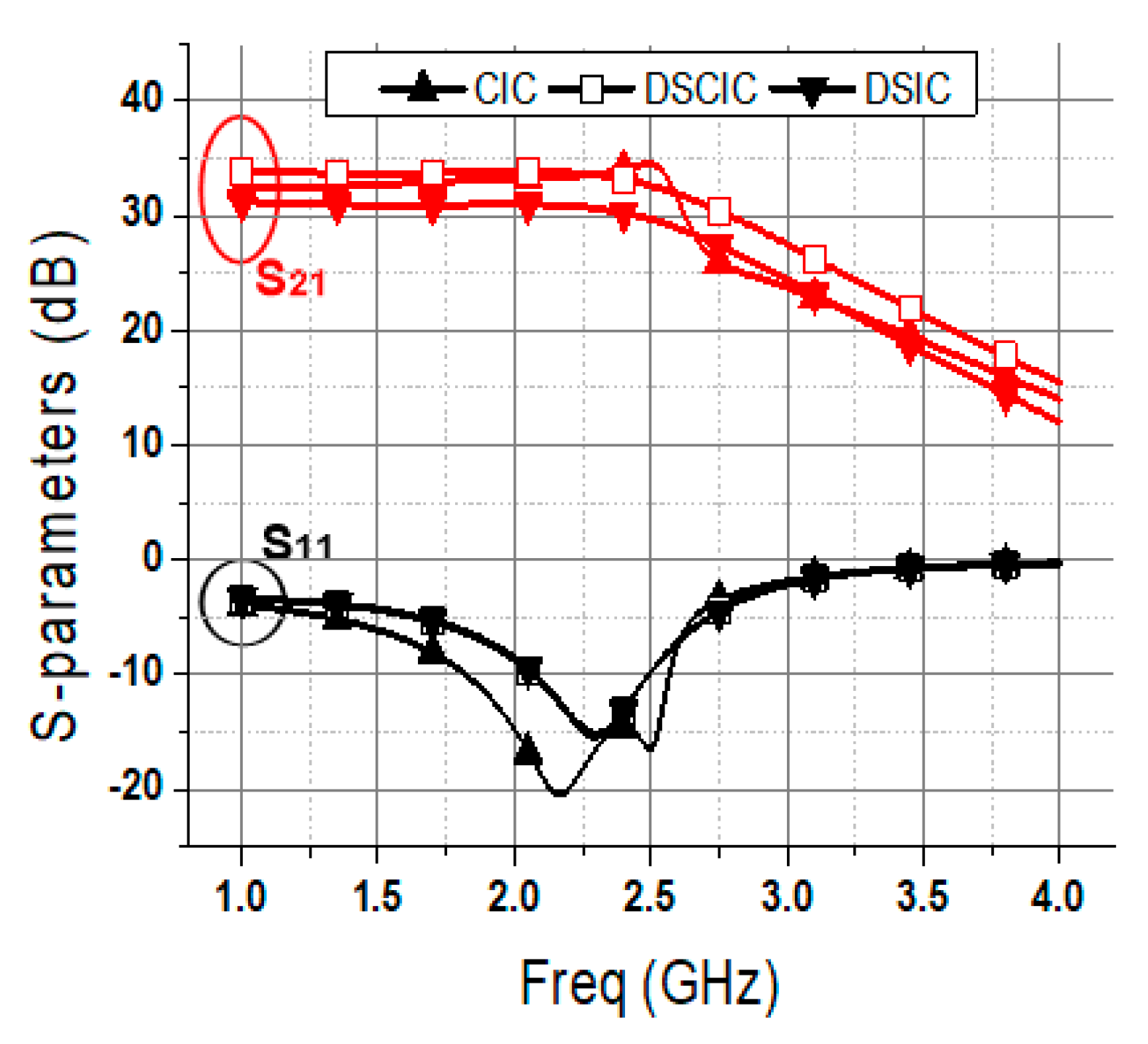
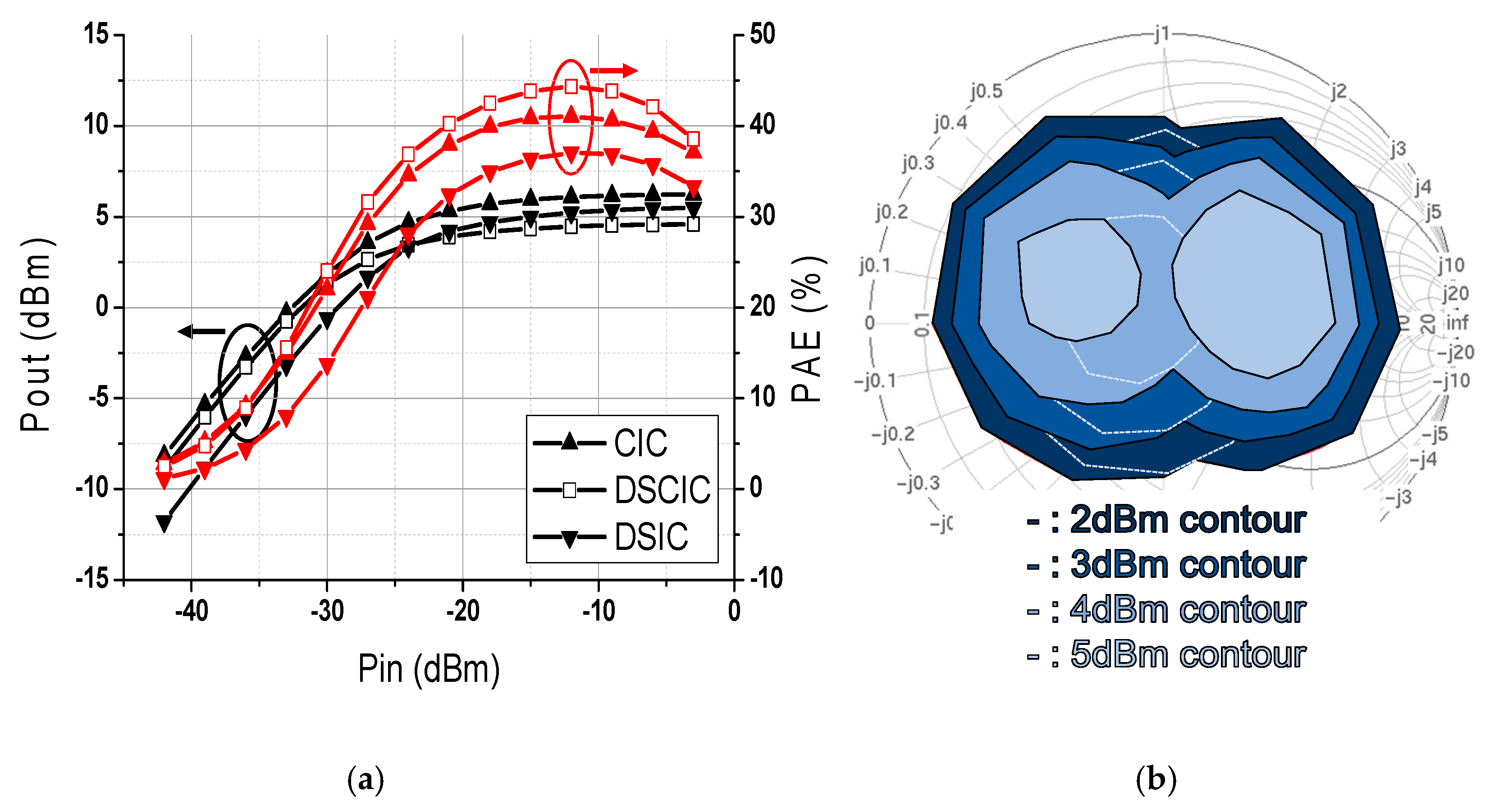
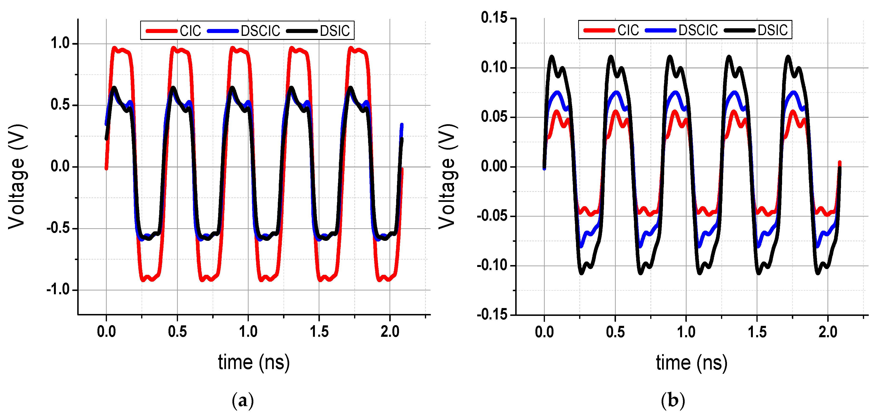
3. Simulation Results

The proposed reconfigurable PA was designed using a 65-nm CMOS process. Because of a standalone circuit pattern, a simple input matching network composed of one series inductor and one shunt capacitor was placed in front of the first DA stage of the proposed PA. Figure 7 shows the simulated forward transmission coefficient (S21) and input reflection coefficient (S11) of the completed PA operated in the cascode inverter configuration (CIC), DSCIC and DSIC. Simulated value for S21 ranges from 30 dB to 35 dB, and the simulated value for S11 is lower than −10 dB at an operating frequency of 2.4 GHz for all three configurations. Figure 8a presents the simulated Psat and PAE of the complete PA in each operation mode.
In the simulation results, the proposed PA operated in CIC, DSCIC and DSIC shows a Psat of +6.1 dBm and a peak PAE of 41.1% under a 100 Ω load impedance, a Psat of +4.5 dBm and a peak PAE of 44.3% under a 50 Ω load impedance, and a Psat of +5.2 dBm and a peak PAE of 37.1% under a 25 Ω load impedance, respectively. Figure 8b shows the simulated total impedance coverage of the proposed reconfigurable PA, while maintaining the output power of greater than +2, +3, +4 and +5 dBm. Compared to conventional inverter-based PAs, impedance coverage is significantly extended, while output power that exceeds the specific power level is maintained without sacrificing power efficiency using only hardware reconfiguration. The proposed PA can compensate for antenna impedance mismatch without any inductors or transformers, and can have the same effect as a TMN at the output stage.
Figure 9a,b show the simulated output voltage waveforms of the complete PA according to the change of circuit configuration under a 200 Ω load impedance and a 5 Ω load impedance, respectively. The RF sinusoidal signal with a power of −10 dBm was applied in order to achieve an output power close to Psat. As predicted, the CIC yields the highest output voltage swing among three configurations when the complete PA directly drives a load impedance greater than 100 Ω, and similarly the DSIC generates the highest output voltage swing among three configurations when it directly drives a load impedance less than 25 Ω. This implies that the proposed reconfigurable PA can change its operation mode automatically over the load impedance variation, by detecting the output voltage swing through a RF envelope detector, and selecting the operation mode to maximize the detector output voltage. Figure 10 shows the possible design for the fully integrated reconfigurable PA, including an automatic tuning circuit. Many researches of [14,15,16] reported an extremely low power RF envelope detector circuit in CMOS at 2.4 GHz frequency band, and most of them adopted the common source-based envelope detector circuit due to high RF-to-DC conversion characteristic. Because the common source-based envelope detectors provide relatively high input impedance, and their power consumption is around microwatt level or below, their effects on the overall RF performance of the proposed PA can be negligible.
Table 1 summarizes and compares the performances of the proposed reconfigurable PA with previously published reports of PAs for ultra-low power (ULP) radios. The simulated PAE at Psat of the proposed PA under all load conditions (100, 50 and 25 Ω) is higher than seen in previously reported PAs, and is achieved without the use of the on-chip matching network at the output stage. The proposed PA can minimize the degradation of the output power under the worst antenna impedance mismatch conditions, and will become a good candidate for miniaturized high-efficiency PAs for ULP short-range wireless communication systems.

4. Conclusions

The reconfigurable CMOS inverter-based stacked power amplifier (PA) is implemented using a 65-nm CMOS process technology, and extends impedance coverage, while maintaining an output power that exceeds the specific power level in the worst antenna impedance mismatch conditions. The proposed PA can minimize the degradation of output power, and can have the same effect as a TMN at the output stage, without the use of inductors or transformers. Because the proposed PA can be easily implemented using a low cost digital CMOS process, while exploiting the advantage of technology scaling, it will become a good solution for miniaturized high-efficiency PAs for ULP radio applications.

Author Contributions

Conceptualization, D.-M.K., H.-G.J. and D.I.; Investigation, D.-M.K., D.K. and D.I.; Supervision, H.-G.J. and D.I.; Writing—original draft, D.-M.K. and D.I. All authors have read and agreed to the published version of the manuscript.

Funding

This research was funded by research funds of Jeonbuk National University in 2015. This research was also funded by Institute for Information and Communications Technology Promotion (IITP) grant funded by the Korea Government (MSIT) (No. 2018-0-01461) and Basic Science Research Program through the National Research Foundation of Korea (NRF) funded by the Ministry of Education (2018R1A2B6008816).

Acknowledgments

This work was supported by research funds of Jeonbuk National University in 2015. This work was also supported by Institute for Information and Communications Technology Promotion (IITP) grant funded by the Korea Government (MSIT) (No. 2018-0-01461) and Basic Science Research Program through the National Research Foundation of Korea (NRF) funded by the Ministry of Education (2018R1A2B6008816). The CAD tool was supported by IDEC.

Conflicts of Interest

The authors declare no conflict of interest.

References

  1. Keerti, A.; Pham, A.-V.H. RF characterization of SiGe HBT power amplifiers under load mismatch. IEEE Trans. Microw. Theory Tech. 2007, 55, 207–214. [Google Scholar] [CrossRef]
  2. Yoon, Y.; Kim, H.; Kim, H.; Lee, K.; Lee, C.; Kenney, J.S. A 2.4-GHz CMOS power amplifier with an integrated antenna impedance mismatch correction system. IEEE J. Solid State Circuits 2014, 49, 608–621. [Google Scholar] [CrossRef]
  3. Song, H.; Bakkaloglu, B.; Aberle, J.T. A CMOS adaptive antenna-impedance-tuning IC operating in the 850MHz-to-2GHz band. In Proceedings of the IEEE International Solid-State Circuits Conference—Digest of Technical Papers, San Francisco, CA, USA, 8–12 February 2009; pp. 384–385. [Google Scholar]
  4. Jeon, J.; Kang, M. A ruggedness improved mobile radio frequency power amplifier module with Dynamic impedance correction by software defined atomization. Electronics 2019, 8, 1317. [Google Scholar] [CrossRef] [Green Version]
  5. Sjöblom, P.; Sjöland, H. An adaptive impedance tuning CMOS circuit for ISM 2.4-GHz band. IEEE Trans. Circuits Syst. I Reg. Pap. 2005, 52, 1115–1124. [Google Scholar]
  6. Shen, Q.; Barker, S. Distributed MEMS tunable matching network using minimal-contact RF-MEMS varactors. IEEE Trans. Microw. Theory Tech. 2006, 54, 2646–2658. [Google Scholar] [CrossRef]
  7. Schmidt, M.; Lourandakis, E.; Leidl, A.; Seitz, S.; Weigel, R. A comparison of tunable ferroelectric Π- and T-matching networks. In Proceedings of the European Microwave Conference, Munich, Germany, 9–12 October 2007; pp. 98–101. [Google Scholar]
  8. Retz, G.; Shanan, H.; Mulvaney, K.; O’Mahony, S.; Chanca, M.; Corwley, P.; Billon, C.; Khan, K.; Quinlan, P. A Highly Integrated Low-Power 2.4GHz Transceiver Using a Direct-Conversion Diversity Receiver in 0.18 μm CMOS for IEEE 802.15.4 WPAN. In Proceedings of the IEEE International Solid-State Circuits Conference—Digest of Technical Papers, San Francisco, CA, USA, 8–12 February 2009; pp. 414–415. [Google Scholar]
  9. Zolfaghari, A.; Said, M.E.; Youssef, M.; Zhang, G.; Liu, T.T.; Cattivelli, F.; Syllaios, Y.I.; Khan, F.; Fang, F.Q.; Wang, J.; et al. A Multi-Mode WPAN (Bluetooth, BLE, IEEE 802.15.4) SoC for Low-Power and IoT Applications. In Proceedings of the Symposium on VLSI Circuits, Kyoto, Japan, 5–8 June 2017; pp. 74–75. [Google Scholar]
  10. Yang, W.; Hu, D.Y.; Lam, C.K.; Cui, J.Q.; Soh, L.K.; Song, D.C.; Zhong, X.W.; Hor, H.C.; Heng, C.L. A +8 dBm BLE/BT Transceiver with Automatically Calibrated Integrated RF Bandpass Filter and −58 dBc TX HD2. In Proceedings of the IEEE International Solid-State Circuits Conference—Digest of Technical Papers, San Francisco, CA, USA, 11–15 February 2017; pp. 136–137. [Google Scholar]
  11. Paidimarri, A.; Nadeau, P.; Mercier, P.; Chandrakasan, A. A 2.4 GHz Multi-Channel FBAR-based Transmitter with an Integrated Pulse-Shaping Power Amplifier. IEEE J. Solid State Circuits 2013, 48, 1042–1054. [Google Scholar] [CrossRef]
  12. Kiumarsi, H.; Mizuochi, Y.; Ito, H.; Ishihara, N.; Masu, K. A Three-stage inverter-based stacked power amplifier in 65 nm complementary metal oxide semiconductor process. Jpn. J. Appl. Phys. 2012, 51, 02BC01. [Google Scholar] [CrossRef]
  13. Van Langevelde, R.; van Elzakker, M.; Van Goor, D.; Termeer, H.; Moss, J.; Davie, A.J. An ultra-low-power 868/915 MHz RF transceiver for wireless sensor network applications. Proceedings of IEEE Radio Frequency Integrated Circuits Symposium, Boston, MA, USA, 7–9 June 2009. [Google Scholar]
  14. Cheng, K.; Chen, S. An ultralow-power wake-up receiver based on direct active RF detection. IEEE Trans. Circuits Syst. I Reg. Pap. 2017, 64, 1661–1672. [Google Scholar] [CrossRef]
  15. Chen, S.; Yang, C.; Cheng, K. A 4.5 μW 2.4 GHz wake-up receiver based on complementary current-reuse RF detector. In Proceedings of the IEEE International Symposium on Circuits and Systems (ISCAS), Lisbon, Portugal, 24–27 May 2015; pp. 1214–1217. [Google Scholar]
  16. Zhou, Y.; Chia, M. A low-power ultra-wideband CMOS true RMS power detector. IEEE Trans. Microw. Theory Tech. 2008, 56, 1052–1058. [Google Scholar] [CrossRef]
  17. Prummel, J.; Papamichail, M.; Ancis, M.; Willms, J.; Todi, R.; Aartsen, W.; Kruiskamp, W.; Haanstra, J.; Opbroek, E.; Rievers, S.; et al. A 10 mW bluetooth low-energy transceiver with on-chip matching. IEEE J. Solid State Circuits 2015, 50, 3077–3088. [Google Scholar] [CrossRef]
  18. Sano, T.; Mizokami, M.; Matsui, H.; Ueda, K.; Shibata, K.; Toyota, K.; Saitou, T.; Sato, H.; Yahagi, K.; Hayashi, Y. A 6.3mW BLE transceiver embedded RX image-rejection filter and TX harmonic-suppression filter reusing on-chip matching network. In Proceedings of the IEEE International Solid-State Circuits Conference—(ISSCC) Digest of Technical Papers, San Francisco, CA, USA, 22–26 February 2015; pp. 240–241. [Google Scholar]
  19. Masuch, J.; Delgado-Restituto, M. A 1.1-mW-RX 81.4 dBm sensitivity CMOS transceiver for bluetooth low energy. IEEE Trans. Microw. Theory Tech. 2013, 61, 1660–1673. [Google Scholar] [CrossRef]
Figure 1. (a) Schematic of a conventional three-stage inverter-based power amplifier (PA) and (b) its output voltage swing limitation.
Electronics 09 00562 g001
Figure 2. Simulation results of the three-stage inverter-based PA using regular-Vth metal-oxide-semiconductor field-effect transistors (MOSFETs) and high-Vth MOSFETs: (a) saturated output power (Psat), PAE, and (b) the power contour.
Electronics 09 00562 g002
Figure 3. Proposed reconfigurable cascode inverter-based stacked PA with three operation modes: cascode inverter configuration, double-stacked cascode inverter configuration and double-stacked inverter configuration.
Electronics 09 00562 g003
Figure 4. Load-pull simulation results of the proposed reconfigurable PA for the three modes: (a) cascode inverter configuration, (b) double-stacked cascode inverter configuration, and (c) double-stacked inverter configuration. The contour starts from an output power of 0 dBm (red circle), and the contour levels are in steps of 1 dB.
Electronics 09 00562 g004
Figure 5. Simulated (a) output voltage waveform, (b) source-to-drain voltage waveforms driven by MP1 and MP2 (vsd,P1 and vsd,P2), and drain-to-source voltage waveforms driven by MN2 and MN1 (vds,N2 and vds,N1) when the proposed PA in the cascode inverter configuration generates an output power of +3 dBm under a 100 Ω load impedance.
Electronics 09 00562 g005
Figure 6. Simulated output impedance of the PA with double-stacked cascode inverter configuration (DSCIC) and double-stacked inverter configuration (DSIC).
Electronics 09 00562 g006
Figure 7. Simulated S-parameters of the proposed reconfigurable PA operated in the cascode inverter configuration (CIC), DSCIC, and DSIC.
Electronics 09 00562 g007
Figure 8. Simulated (a) Psat and PAE of the complete PA in each operation mode and (b) total impedance coverage of the proposed reconfigurable PA while maintaining an output power of greater than +2, +3, +4, and +5 dBm.
Electronics 09 00562 g008
Figure 9. Simulated output voltage waveforms of the complete PA according to the change of circuit configuration under (a) a 200 Ω load impedance and (b) a 5 Ω load impedance. The RF sinusoidal signal with a power of −10 dBm was applied in order to achieve an output power close to Psat.
Electronics 09 00562 g009
Figure 10. Possible design for the fully integrated reconfigurable PA including an automatic tuning circuit.
Electronics 09 00562 g010
Table 1. Comparison of performances of the proposed reconfigurable PA with previously published reports of PAs for ultra-low power (ULP) radios.
PA1 Proposed PA2 [17]2 [18]2 [19]
CICDSCICDSIC
CMOS Technology
(nm)
655540130
Supply Voltage
(V)
2.40.9–3.31.11
Output Matching NetworkNoYesYesYes
Saturated Power (Psat)
(dBm)
+6.1+4.5+5.2001.6
PA Efficiency @ Psat
(%)
41.1%44.3%37.1%30.0%<30%26.8%
Strongest Harmonic Emission (dBm)3 HD3
−27
3 HD3
−20
3 HD3
−31
4 HD3
−52
4 HD3
−48
4 HD3
−32
Power Consumption
@ Psat (mW)
9.86.28.85 10.15 7.75 5.9
1 Simulation results, 2 Measurement results, 3 Tested at the output power of +2 dBm, 4 Tested at the saturated output power, 5 Total power consumption of whole transmitter (Tx).

