Article

A 12-Bit 200 MS/s Pipelined-SAR ADC Using Back-Ground Calibration for Inter-Stage Gain

National ASIC system engineering research center, Southeast University, Nanjing 210096, China
*
Author to whom correspondence should be addressed.
Electronics 2020, 9(3), 507; https://doi.org/10.3390/electronics9030507
Submission received: 18 February 2020 / Revised: 17 March 2020 / Accepted: 17 March 2020 / Published: 19 March 2020
(This article belongs to the Special Issue Analog/Digital Mixed Circuit and RF Transceiver Design)

Abstract

:
A 12-bit 200 MS/s pipelined successive-approximation-register (SAR) analogue-to-digital-converter (ADC) implemented in 40 nm CMOS is presented. Such an ADC consists of two asynchronous SAR ADCs and a dynamic amplifier, which consumes a static power of 1.2 mW (the total power is 8 mW) and occupies an area of 0.046 mm2. The inter-stage gain is affected by the parasitic capacitance in SAR ADCs as well as the gain of the dynamic amplifier, which is variable with respect to process-voltage-temperature (PVT). A background calibration of the inter-stage gain is proposed to adjust the inter-stage gain and to track the PVT variables. The measurement results show that, with calibration, the spurious-free-dynamic-range (SFDR) and signal-to-noise-and-distortion-ratio (SINAD) can be improved from 68 dB and 61 dB to 78 dB and 63 dB, respectively. The dynamic performance was stable under different VT conditions.

1. Introduction

Successive-approximation-register (SAR) ADC is quite powerful and area-efficient due to its mostly digitized structure [1,2], which is scalable with respect to process development. Nonetheless, the bit-by-bit operation sequence limits its sampling rate and the comparator noise confines the overall signal-noise-ratio (SNR) [3,4]. The traditional pipelined structure has a speed merit, but the multiple amplifiers consume much power. Recently, pipelined-SAR structure has obtained much attention because it combines both the merits of pipelines and SAR ADCs [5,6,7,8,9,10,11,12,13,14,15,16,17]. As in traditional pipelined ADCs, two SAR ADCs connected by a residue amplifier (RA) can work concurrently. The pipelined-SAR ADC usually employs merely one amplifier, since each SAR ADC can resolve more bits than in a conventional pipelined structure with flash sub-ADC. The RA can reduce the input referred noise of the second SAR ADC, thus greatly relaxing its design burden and decreasing its power. A dynamic residue amplifier (DRA) is usually employed due to its simple structure and zero static power [15,16,17,18]. In a dynamic amplifier, the output voltage swing needs to be kept in a small range to obtain relatively high linearity. Fortunately, in a pipelined-SAR ADC, the residue voltage of the first stage (which is also the input of the dynamic amplifier) is usually smaller than the pipelined counterpart. Further, the integration process assists to filter the amplifier noise. The side effect of an open-loop structure of a DRA is also obvious. Its gain is inaccurate and variable due to PVT changes. Calibration schemes have often been employed in pipelined-SAR ADCs to remedy this issue. In [19], a dither signal was injected into the key path to obtain a bit-weights background. Nevertheless, the calibration converged slowly due to large signal-dependent interferences. In [20], the gain was adjusted according to the induced gain-mismatch error, but this was unsuitable for dynamic amplifiers that work under a foreground mode. In [17], the gain of the dynamic amplifier was determined by capacitor ratios, which were stable under various PVT conditions but at the cost of a large analog overhead.
In this work, a simple but efficient background scheme is proposed to adjust inter-stage gain and obtain the proper value. On the other hand, this calibration scheme works in the background, so as to track PVT variations. It adds only a small analog overhead. In Section 2, the ADC architecture and timing relationship are depicted. Section 3 provides the principle and circuit implementation of the background calibration. The measurement results are given in Section 4. Finally, a conclusion is drawn in Section 5.

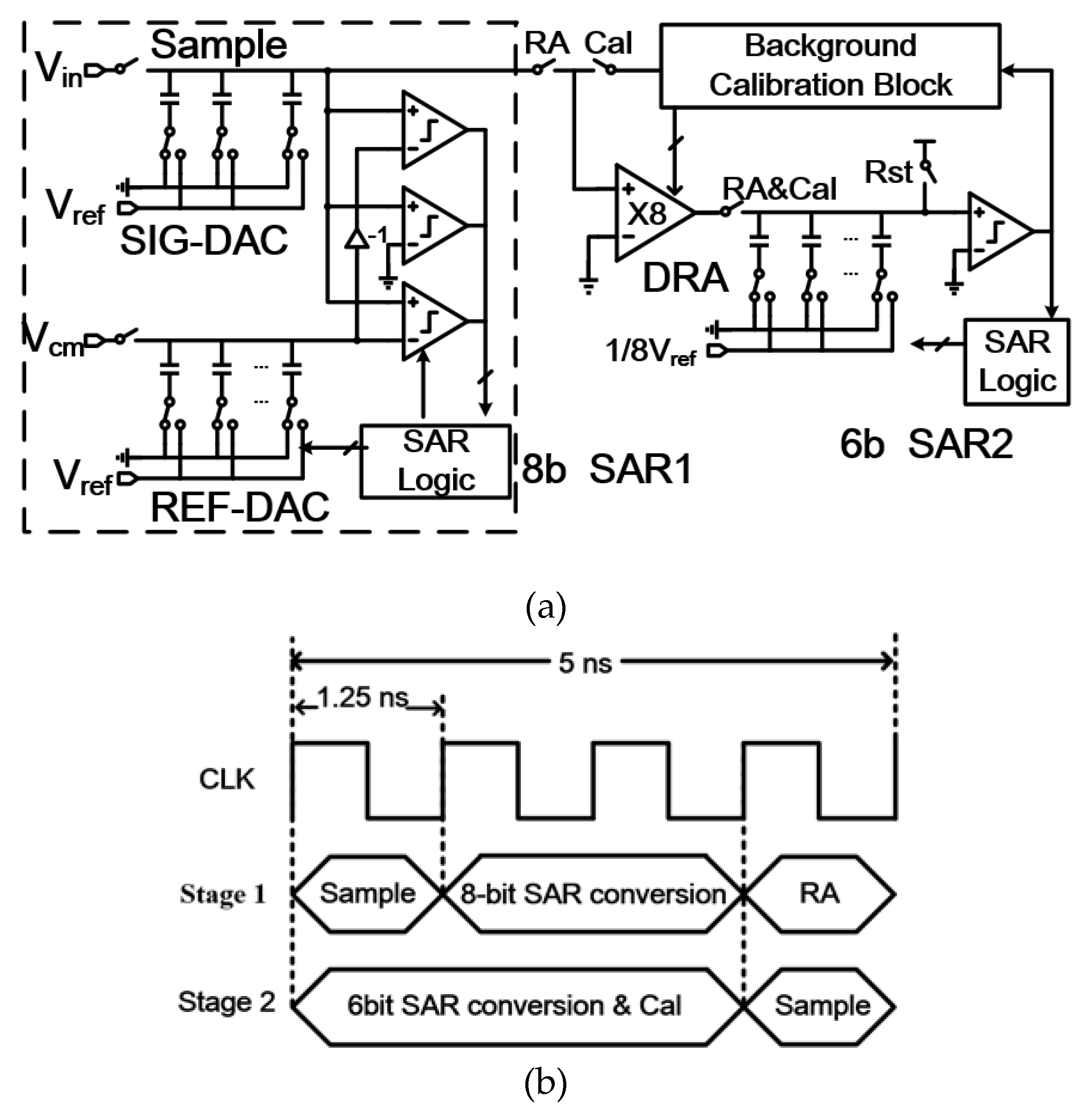
2. Architecture of the Proposed ADC

The block diagram is shown in Figure 1a, in which an 8-bit front-end SAR (SAR1) and 6-bit back-end SAR (SAR2) are connected by the dynamic residue amplifier (DRA). The residue of SAR1 is quite small due to the 8-bit quantization, which confines both the input and output range of the DRA, thereby improving its linearity. Unlike traditional SAR ADC, the signal sampling and residue amplifying phases are included in SAR1, thus decreasing its conversion time interval. Herein, we employ a 2-bit/cycle structure as the first stage to double the conversion speed [3]. The SAR1 includes signal digital-to-analogue converter (SIG-DAC) and reference digital-to-analogue converter (REF-DAC).The timing diagram is illustrated in Figure 1b. The input clock frequency is 800 MHz, which is employed to generate several 200 MHz clock phases for sampling, conversion and residue amplification. As illustrated in Figure 1b, the input clock period is 1.25 ns and it takes four cycles to complete one conversion, in which one cycle is allocated to signal sampling, two cycles are allocated to 8-bit asynchronous SAR1 and one cycle is allocated to the DRA. Since SAR2 takes three cycles (3.75 ns) to finish one conversion, a traditional asynchronous 1-bit/cycle structure can meet the speed demand. The background calibration of the inter-stage gain is started right after the 6-bit SAR conversion.
The reference voltage of SAR1 (Vref1) is the power supply (1.1 V). Hence, SAR1 generates a residue that is confined to ±4.3 mV. A 2-bit redundancy (12.9 mV) is included to tolerate various dynamic errors, and finally 12-bit data are acquired. Originally, 2-bit redundancy and 8-bit SAR1 requires that the DRA provide 64x gain. To confine the output range of the DRA and achieve high linearity, only 8× gain is allocated to the DRA. Accordingly, the reference voltage of SAR2 (Vref2) is 1/8 Vref1. The offsets of the three comparators of SAR1 ADC occupy some inter-stage redundancy. The offset mismatch of the DRA and comparators is amplified by the inter-stage 8x gain, which can easily cause the residue output to exceed the redundancy range. To remedy this issue, the offsets of comparators and the DRA are all foreground calibrated [10]. The offset of the comparator in SAR1 is calibrated by resetting the inputs to a common mode voltage. The comparator output is feedback to a DAC. The offset voltages of the residue amplifier and the comparator in SAR2 are calibrated together in a similar way. Finally, 2-bit redundancy is employed to tolerate the dynamic errors such as reference settling and kick-back effects. The capacitor mismatches between the reference DAC and signal DAC are also corrected by the 2-bit redundancy.

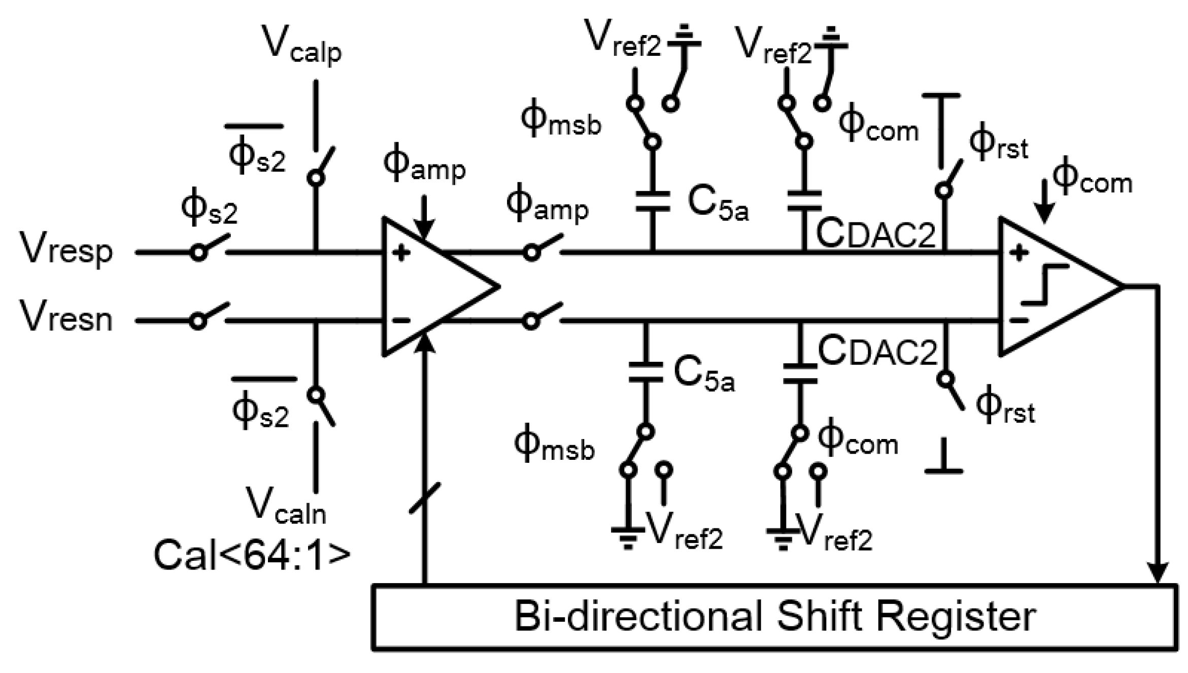
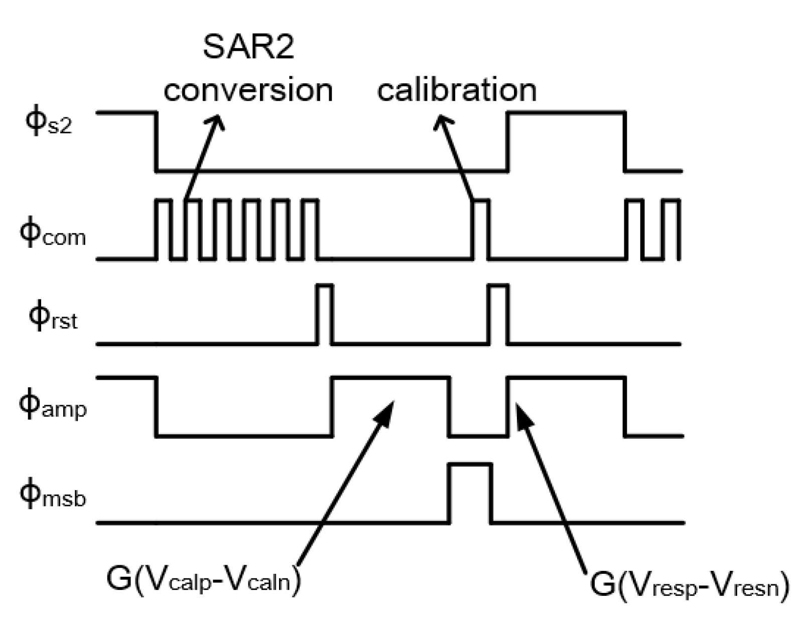
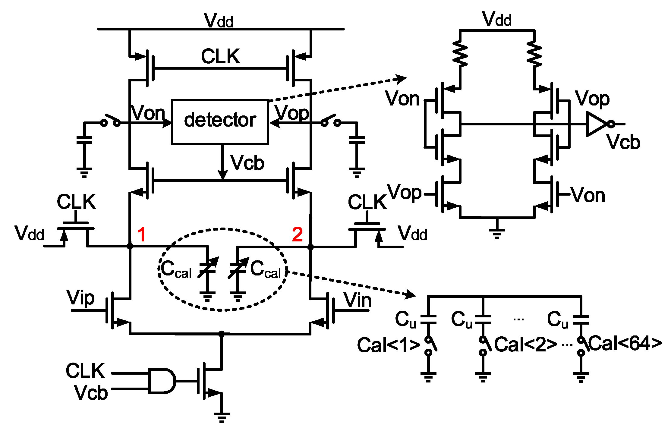
3. Background Calibration of the Inter-Stage Gain

VFS1 and VFS2 are the signal ranges of the two SAR ADCs, respectively. M, R and G are on behalf of the SAR1 bit, the redundancy bit and the inter-stage gain. Ideally, these variables should meet the below relationship:
G × V F S 1 2 M R = V F S 2
If G is larger than the ideal value, missing analog information occurs. If G is smaller, missing codes occur [20]. In both cases, obvious nonlinearity is induced. On the other side, G of the DRA is changeable due to PVT variations. As a result, calibration for accurate G should be in real-time. The key idea herein is to compare the left side to the right side in Equation (1). The comparison result is fed to the DRA so as to adjust the gain until they are almost equal.
As illustrated in Figure 2, only the DRA and part of SAR2 related to the proposed calibration are shown. The corresponding timing diagram is depicted in Figure 3. Compared to the traditional pipelined-SAR ADC, some switches and phases are added. The DRA is disconnected to SAR1 after its residue voltage is amplified and sampled by the DAC of SAR2 (CDAC2). Then, SAR2 conversion begins. Afterward, its DAC is reset to the power supply. The DRA starts again to amplify the calibration voltage (Vcalp − Vcaln) to obtain G × (Vcalp − Vcaln), which is also sampled by the CDAC2. The bottom plate of C5a is switched from Vref2 to ground. Finally, the comparator works, and the result is fed to a bi-directional shift register (BDSR) to adjust G. Since the switching method of SAR2 is a split structure [21], C5a is a quarter of the total capacitor of CDAC2. Herein, Vcalp − Vcaln is set at VFS1/29 and (M − R) equals 6. The calibration voltage (Vcalp − Vcaln) is generated by the reference voltage Vref1 and a resistor array. The resistor ratio makes the calibration voltage stable. The mismatch of the resistors affects the calibration accuracy slightly. A Monte Carlo simulation is performed using 1000 runs, as shown in Figure 4. The mismatch of the resistor is 1%, and the induced three-sigma value of the deviation of Vcalp − Vcaln is 120 μV, which is smaller than half of the least-significant-bit (LSB) of the whole ADC.
The comparison result is equivalent to Equation (1), which can be derived from
G × V F S 1 2 M R V F S 2 G × ( V c a l p V c a ln ) V F S 2 / 8
As a result, when the comparison result is 1, it means G is larger than the ideal value, and vice versa. The DRA adopts a traditional structure, except that we add a pair of capacitor arrays (64 capacitor units) at nodes 1 and 2. The common-mode detector determines when the DRA is cut off by employing the signal Vcb. When the comparison result is 1 (or 0), it means G is larger (smaller) than the ideal value. One of the calibration capacitors is then disconnected (added), which can decrease (increase) G by shortening (enlarging) the integrating time. The gain of this cascode DRA is
G = 2 ( V d d V c m ) V g t ( 1 + C 1 C 2 )
where Vdd and Vcm are determined at the system design level. Vgt is the over-driving voltage, which is 100 mV–200 mV, thereby keeping the transistors in a saturation state and ensuring enough voltage swing. C1 is the sum of parasitic capacitance and the calibration capacitance at nodes 1 and 2 while C2 is the parasitic capacitance and the sampling capacitance of SAR2 (Figure 5).
The cascode structure, which contains a detector, the clock (CLK) and the controlling signal (Vcb), improves the gain relative to the traditional one by adding a factor decided by the capacitor ratio. Herein, the calibration capacitor array (Ccal) is added to obtain the desired gain value. Although this calibration capacitor array would change the speed of the DRA, its maximum operation time (0.78 ns) is still smaller than the allocated time (one cycle = 1.25 ns).
Each unit capacitor is 1.3 fF and the total capacitance is about 66 fF. In the beginning, half of the capacitors are connected, then the bi-directional shift register (BDSR) with the comparison result directs whether to add or subtract. Simulation results show that G can vary from 8.06 to 10 while the operation time does not exceed the total calibration interval. The spurious-free-dynamic-range (SFDR) performances before and after inter-stage gain calibration at several different corners are listed in Figure 6, which shows the robustness of the proposed scheme.
The BDSR consists of a series of mux and flip-flops. A 4-bit version is illustrated in Figure 7, although the 64-bit one is employed. The Sel signal from the comparator selects whether 0 or 1 is passed. If Sel is 0, then the outputs of flip-flops move right and 0 is given to Cal<4>. On the contrary, if Sel is 1, the flip-flop outputs move left and 1 is given to Cal<1>.

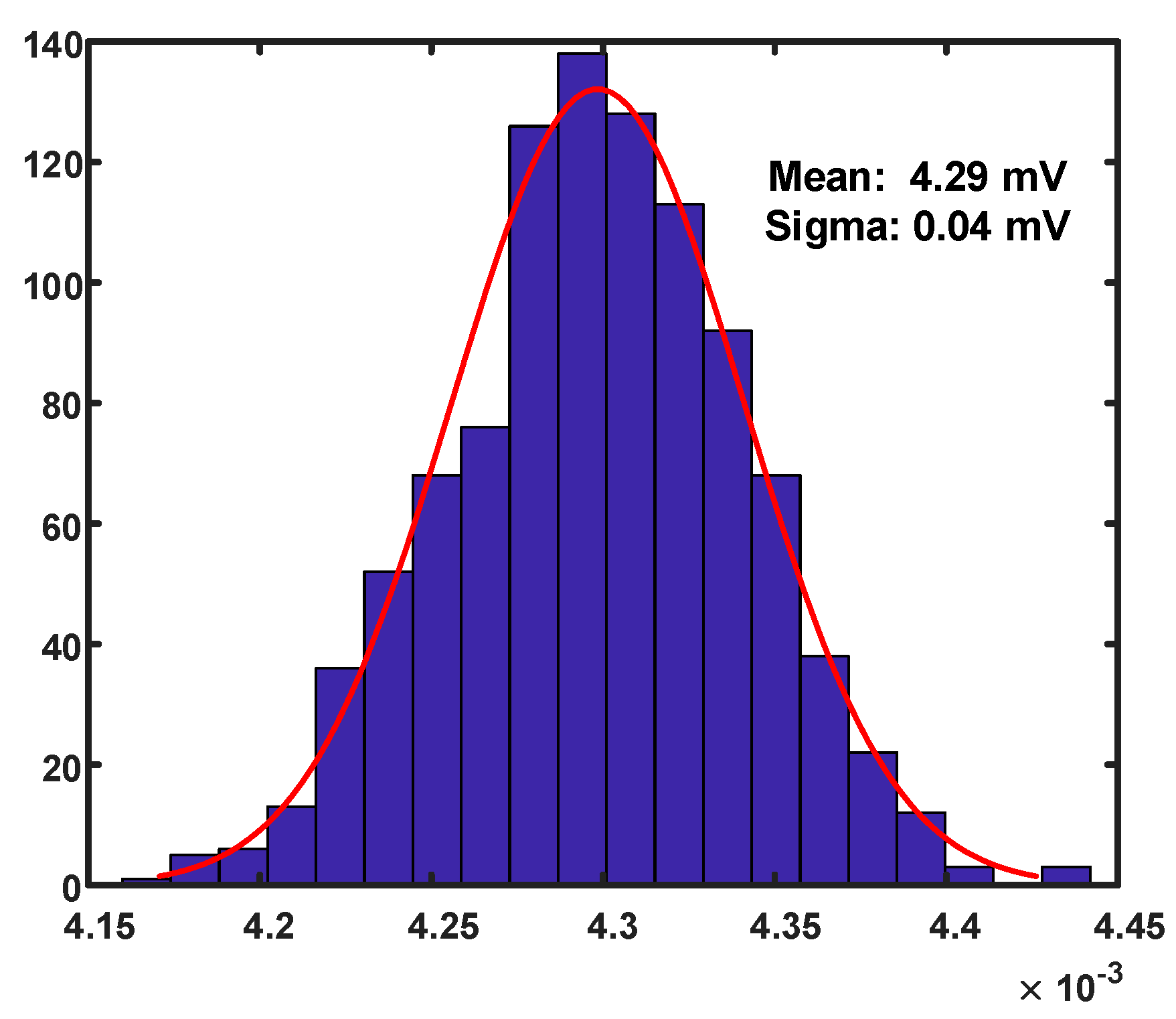
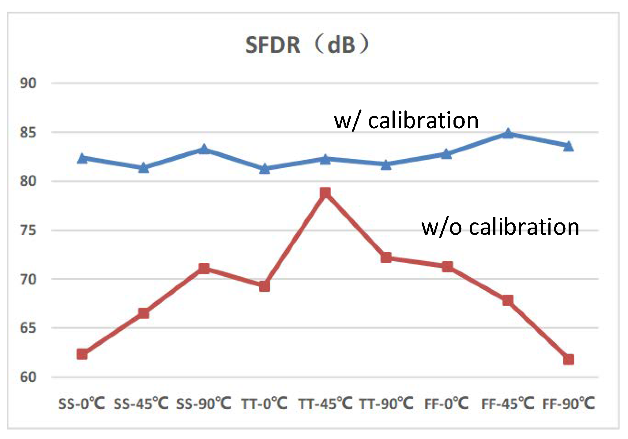
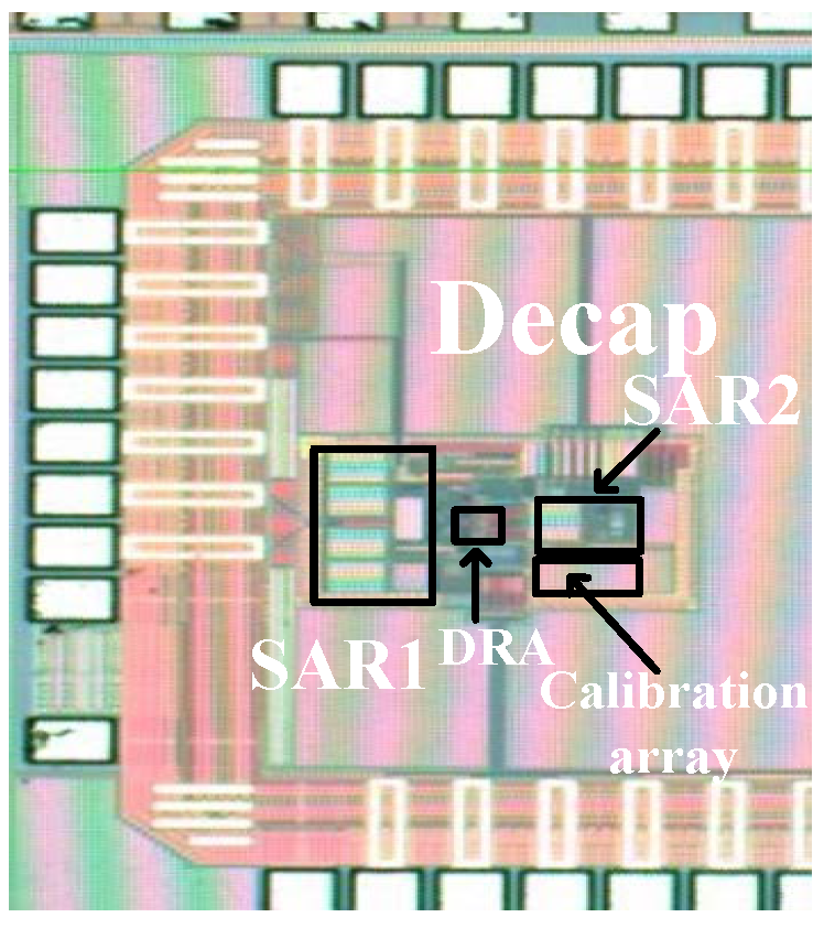
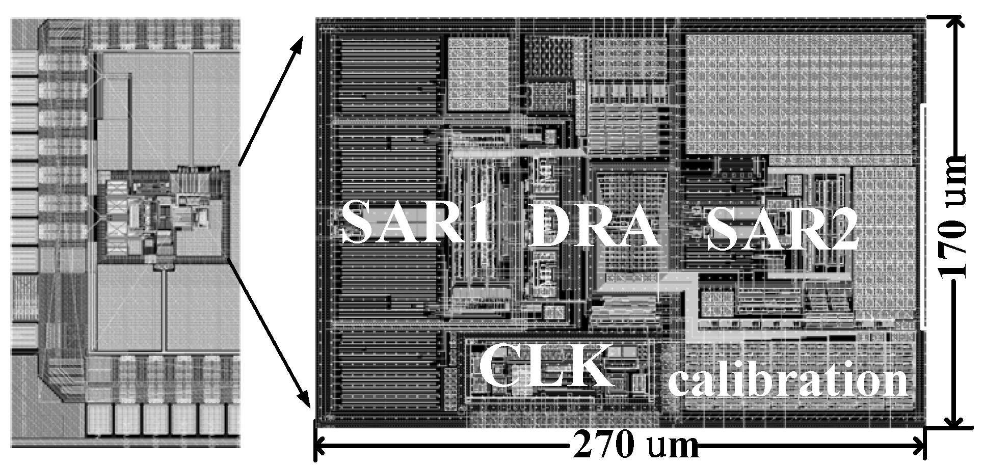
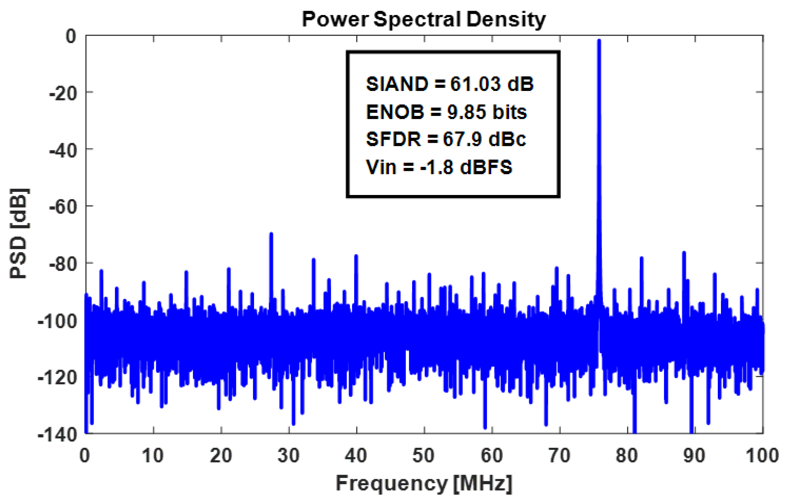
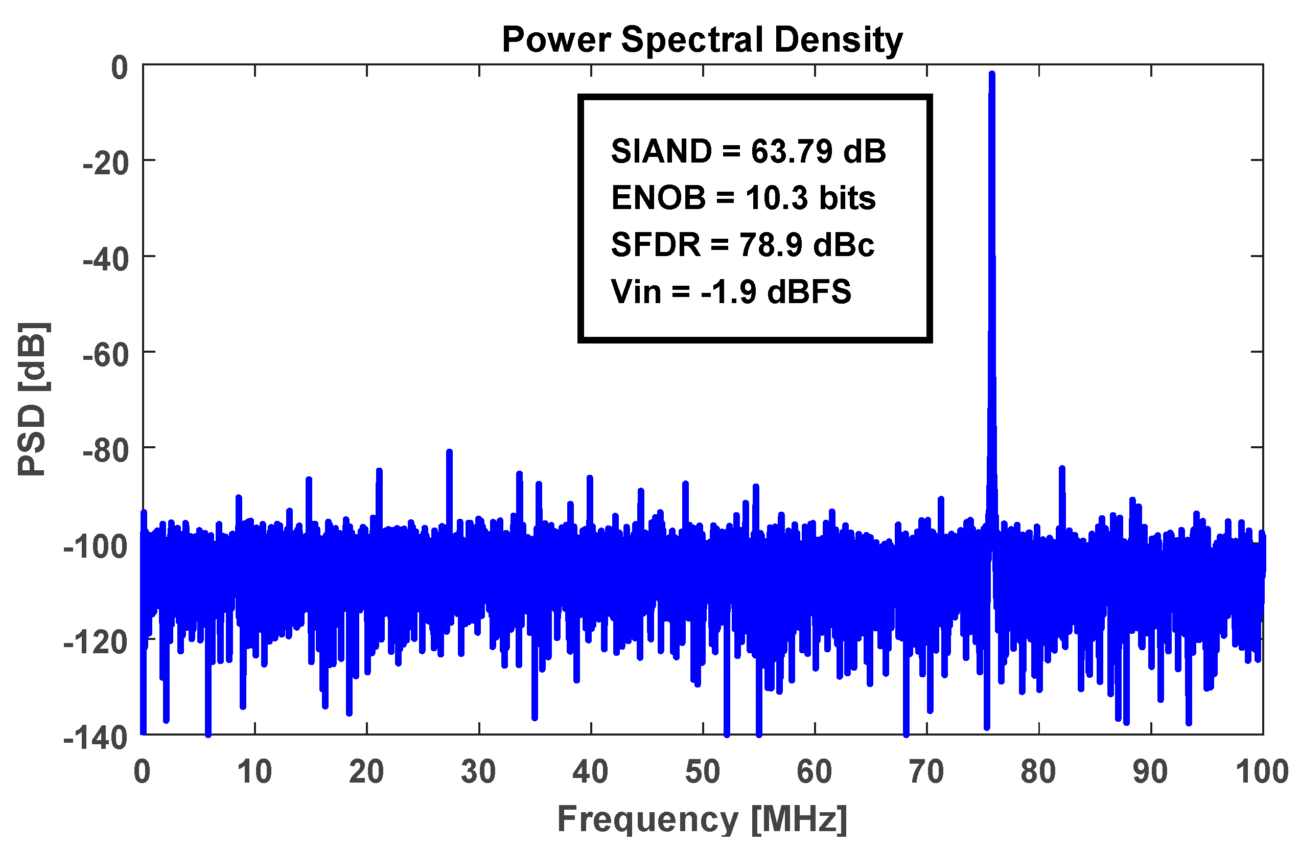
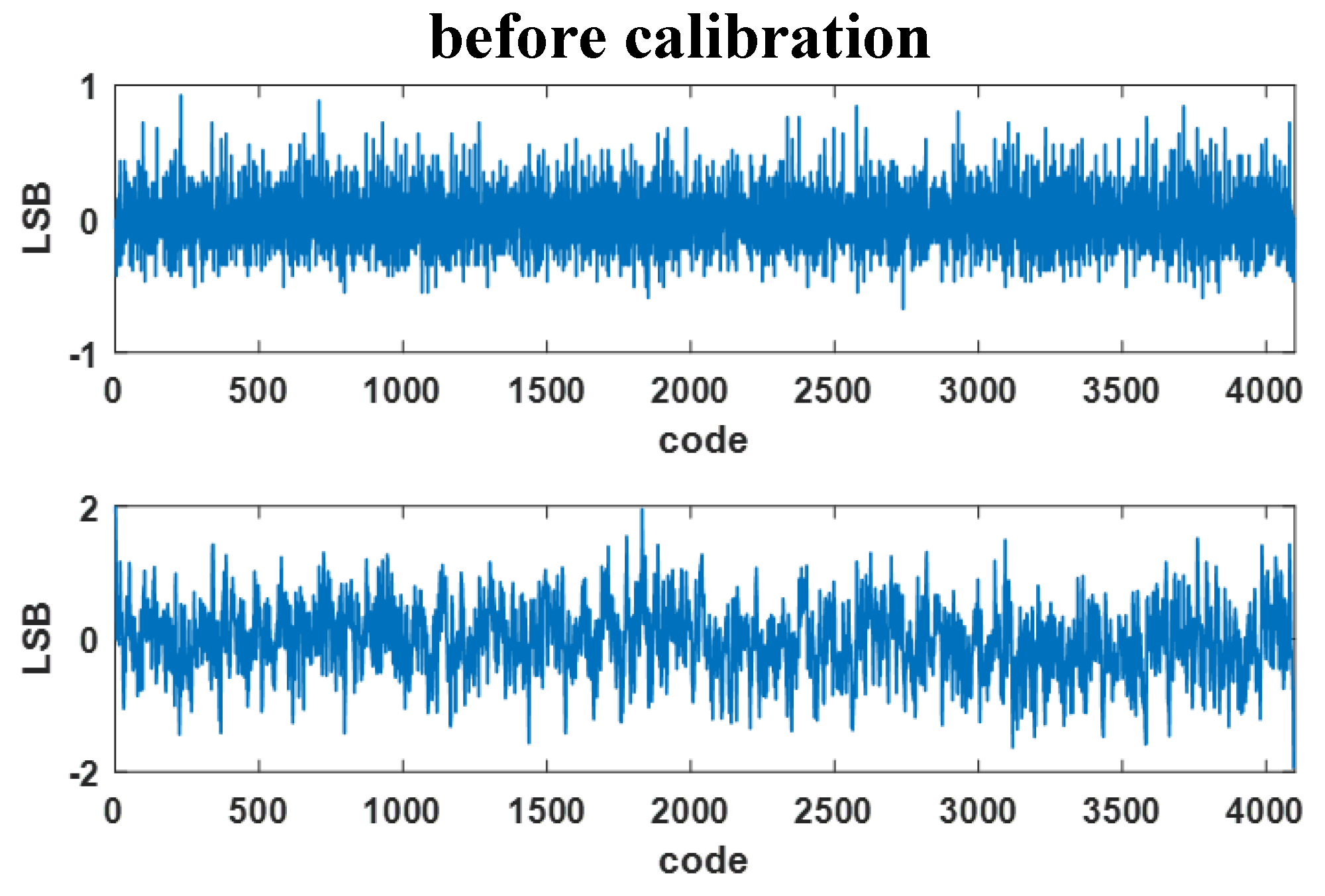
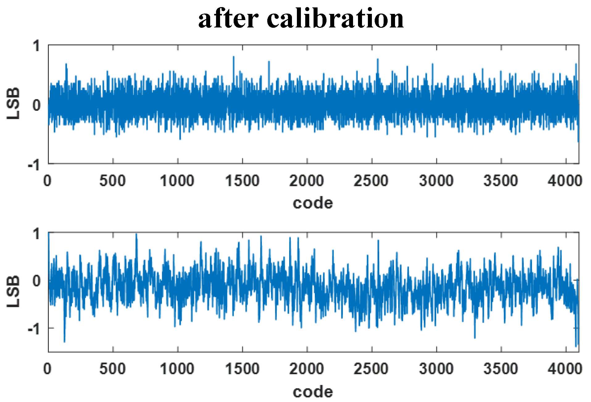
4. Measurement Results

The pipelined-SAR ADC with the proposed background calibration is fabricated on a 40-nm low power (LP) process. The chip photo and its layout graph are shown in Figure 8 and Figure 9, respectively, which occupies about 270 × 170 um. The total power consumption of the ADC core is about 8 mW, including the clock generators.
With 75 MHz input, the signal-to-noise-and-distortion-ratio (SINAD) is improved from 61 dB to 63 dB, and the SFDR is improved from 68 dB to 78 dB, using the proposed calibration, as shown in Figure 10 and Figure 11, respectively. The effective-number-of-bits (ENOB) is also increased. The gain deviation causes large integral-nonlinearity (INL) degradation at several dis-continuities due to the pipelined-SAR structure. After calibration, differential-nonlinearity (DNL) is improved from 0.9 (least-significant-bit) LSB/−0.5LSB to 0.7LSB/−0.3LSB, and INL is improved from 1.9LSBs/−1.89LSBs to 1 LSB/−1.2LSBs, as illustrated in Figure 12 and Figure 13, respectively.
To verify the calibration in real-time, the chip was measured under different power supplies and temperatures. It can be seen that the dynamic performance keeps stable under a wide range of conditions. The SFDR value changed about 1 dB, and the SINAD changed by nearly 0.3 dB under a 1 to 1.2 V supply, as seen in Figure 14. From 0 to 80 °C, the SFDR varied about 2.4 dB, while the SINAD changed about 1.5 dB, as in Figure 15. The Walden figure of merit (FOM) could achieve 31.7 fj/conv-step, which is quite competitive.
In Table 1, the indexes are compared with the state of art works. Compared to [20], this calibration operates in the background and can converge faster than the method in [19], since no dither is injected. The dynamic performance of [17] probably behaved better, and could also converge quite fast without any dither injection. Nonetheless, it consumed large analog overhead. Comprehensively, the proposed calibration can track PVT variations and greatly improve dynamic performance with small overhead.

5. Conclusions

A 12-bit 200 MS/s pipelined-SAR ADC implemented on 40 nm CMOS process was presented. This ADC reuses the comparator of SAR2 to obtain information of the adjustment direction of G in the dynamic amplifier, thus avoiding complex digital calibration or large overhead. The proposed calibration operated in the background and improved SFDR and SINAD by 78.9 and 63.7 dB, respectively. This improvement was also stable under various conditions, and the total power consumption was 8 mW, achieving a 31.7 fj/conv-step Walden FOM.

Author Contributions

Conceptualization, J.W. (Junjie Wu) and J.W. (Jianhui Wu); Data curation, J.W. (Junjie Wu) and J.W. (Jianhui Wu); Funding acquisition, J.W. (Junjie Wu) and J.W. (Jianhui Wu); Investigation, J.W. (Junjie Wu) and J.W. (Jianhui Wu); Methodology, J.W. (Junjie Wu) and J.W. (Jianhui Wu); Resources, J.W. (Junjie Wu) and J.W. (Jianhui Wu); Writing—original draft, J.W. (Junjie Wu) and J.W. (Jianhui Wu); Writing—review & editing, J.W. (Junjie Wu) and J.W. (Jianhui Wu). All authors have read and agreed to the published version of the manuscript.

Funding

This work is supported by the National Natural Science Foundation of China under project number No.61401090 and No.61704088.

Conflicts of Interest

The authors declare no conflict of interest. The funders had no role in the design of the study.

References

  1. Kang, H.; Hong, H.; Kim, W.; Ryu, S. A time-interleaved 12-b 270-MS/s SAR ADC with virtual-timing-reference time-skew calibration scheme. IEEE J. Solid-State Circuit 2018, 53, 2584–2594. [Google Scholar] [CrossRef]
  2. Jun, Y.-H.; Huang, H.-Y.; Lee, S.-Y.; Lai, S.C.; Juang, W.H.; Luo, C.H. A self-testing platform with a foreground digital calibration technique for SAR ADCs. Appl. Sci. 2016, 6, 217. [Google Scholar] [CrossRef] [Green Version]
  3. Hong, H.; Kim, W.; Kang, H.; Park, S.J.; Choi, M.; Park, H.J.; Ryu, S.T. A decision-error-tolerant 45 nm CMOS 7b 1 GS/s nonbinary 2b/Cycle SAR ADC. IEEE J. Solid-State Circuit 2015, 50, 543–555. [Google Scholar] [CrossRef]
  4. Chan, C.; Zhu, Y.; Seng, U.; Martins, R.P. A two-way interleaved 7-b 2.4-GS/s 1-then-2 b/Cycle SAR ADC with background offset calibration. IEEE J. Solid-State Circuit 2017, 53, 850–860. [Google Scholar] [CrossRef]
  5. Furuta, M.; Nozawa, M.; Itakura, T. A 10-bit, 40-MS/s, 1.21 mW pipelined SAR ADC using single-ended 1.5-bit/cycle conversion technique. IEEE J. Solid-State Circuit 2011, 46, 1360–1370. [Google Scholar] [CrossRef]
  6. Lim, Y.; Flynn, M. A 1 mW 71.5 dB SNDR 50 MS/s 13 bit fully differential ring amplifier based SAR-assisted pipelined ADC. IEEE J. Solid-State Circuit 2015, 50, 2901–2911. [Google Scholar] [CrossRef]
  7. Martens, E.; Hershberg, B.; Craninckx, J. A 69-dB SNDR 300-MS/s two-time interleaved pipelined SAR ADC in 16-nm CMOS FinFET with capacitive reference stabilization. IEEE J. Solid-State Circuit 2018, 53, 1161–1171. [Google Scholar] [CrossRef]
  8. Brandolini, M.; Shin, Y.; Raviprakash, K.; Wang, T.; Wu, R.; Geddada, H.M.; Ko, Y.J.; Ding, Y.; Huang, C.S.; Shih, W.T.; et al. A 5 GS/s 150 mW 10b SHA-Less pipelined/SAR hybrid ADC for direct-sampling systems in 28 nm CMOS. IEEE J. Solid-State Circuit 2015, 50, 2922–2934. [Google Scholar] [CrossRef]
  9. Zhu, Y.; Chan, C.; Seng, U.; Martins, R.P. A 10-bit 500-MS/s partial-interleaving pipelined SAR ADC with offset and reference mismatch calibrations. IEEE Trans. Very Large Scale Integr. (VLSI) Syst. 2017, 25, 354–363. [Google Scholar] [CrossRef]
  10. Zhu, Y.; Chan, C.; Seng, U.; Martins, R.P. An 11b 450 MS/s three-way time-interleaved subranging pipelined-SAR ADC in 65 nm CMOS. IEEE J. Solid-State Circuit 2016, 51, 1223–1234. [Google Scholar] [CrossRef]
  11. Lin, C.; Lee, T. A 12-bit 210-MS/s 2-times interleaved pipelined-SAR ADC with a passive residue transfer technique. IEEE Trans. Circuits Syst. I Reg. Pap. 2016, 63, 929–938. [Google Scholar] [CrossRef]
  12. Yoshioka, K.; Sugimoto, T.; Waki, N.; Kim, S.; Kurose, D.; Ishii, H.; Furuta, M.; Sai, A.; Itakura, T. A 0.7V 12b 160 MS/s 12.8 fJ/conv-step pipelined-SAR ADC in 28 nm CMOS with digital amplifier technique. In Proceedings of the 2017 IEEE International Solid-State Circuits Conference Digest of Technical Papers, San Francisco, CA, USA, 5–9 February 2017. [Google Scholar]
  13. Kull, L.; Luu, D.; Menolfi, C.; Braendli, M.; Francese, P.A.; Morf, T.; Kossel, M.; Yueksel, H.; Cevrero, A.; Ozkaya, I.; et al. A 10b 1.5GS/s pipelined-SAR ADC with background second-stage common-mode regulation and offset calibration in 14 nm CMOS FinFET. In Proceedings of the 2017 IEEE International Solid-State Circuits Conference Digest of Technical Papers, San Francisco, CA, USA, 5–9 February 2017. [Google Scholar]
  14. Xu, H.; Cai, Y.; Du, L. A 78.5dB-SNDR radiation-and metastability-tolerant two-step split SAR ADC operating up to 75 MS/s with 24.9 mW power consumption in 65 nm CMOS. In Proceedings of the 2017 IEEE International Solid-State Circuits Conference Digest of Technical Papers, San Francisco, CA, USA, 5–9 February 2017. [Google Scholar]
  15. Verbruggen, B.; Iriguchi, M.; Craninckx, J. A 1.7 mW 11b 250 MS/s 2-times interleaved fully dynamic pipelined SAR ADC in 40 nm digital CMOS. IEEE J. Solid-State Circuit 2011, 47, 2880–2887. [Google Scholar] [CrossRef]
  16. Goes, F.; Ward, C.; Astgimath, S.; Yan, H.; Riley, J.; Zeng, Z.; Jan, M.; Wang, S.; Bult, K. A 1.5 mW 68 dB SNDR 80 MS/s 2×Interleaved pipelined SAR ADC in 28 nm CMOS. IEEE J. Solid-State Circuit 2014, 49, 2835–2845. [Google Scholar] [CrossRef]
  17. Huang, H.; Xu, H.; Chiu, Y. A non-interleaved 12-b 330-MS/s pipelined-SAR ADC with PVT-Stabilized dynamic amplifier achieving sub-1-dB SNDR variation. IEEE J. Solid-State Circuit 2017, 52, 3235–3247. [Google Scholar] [CrossRef]
  18. Zhang, M.; Liu, Q.; Fan, X. Gain-boosted dynamic amplifier for pipelined-SAR ADCs. Electron. Lett. 2017, 53, 708–709. [Google Scholar] [CrossRef]
  19. Zhou, Y.; Xu, B.; Chiu, Y. A 12 bit 160 MS/s two-step SAR ADC with background bit-weight calibration using a time-domain proximity detector. IEEE J. Solid-State Circuit 2015, 50, 920–931. [Google Scholar] [CrossRef]
  20. Zhong, J.; Zhu, Y.; Chan, C. A 12b 180 MS/s 0.068mm2 with full-calibration-integrated pipelined-SAR ADC. IEEE Trans. Circuits Syst. I Reg. Pap. 2017, 64, 1684–1695. [Google Scholar] [CrossRef]
  21. Ginsburg, B.; Chandrakasan, A. An energy-efficient charge recycling approach for a SAR converter with capacitive DAC. In Proceedings of the IEEE International Symposium on Circuits and Systems (ISCAS2005), Kobe, Japan, 23–26 May 2005. [Google Scholar]
Figure 1. (a) Block diagram of the proposed ADC; (b) timing diagram of the proposed ADC.
Electronics 09 00507 g001
Figure 2. Circuit schematic of the background calibration.
Electronics 09 00507 g002
Figure 3. Operation timing of the background calibration.
Electronics 09 00507 g003
Figure 4. Monte Carlo simulation of the calibration voltage due to the mismatch of the resistors.
Electronics 09 00507 g004
Figure 5. Circuit schematic of the DRA with calibration capacitors.
Electronics 09 00507 g005
Figure 6. Simulation results of spurious-free-dynamic-range (SFDR) at different corners.
Electronics 09 00507 g006
Figure 7. The 4-bit example of the bi-directional shift register (BDSR).
Electronics 09 00507 g007
Figure 8. Chip photo of the ADC.
Electronics 09 00507 g008
Figure 9. Layout of the proposed ADC.
Electronics 09 00507 g009
Figure 10. Dynamic performances before calibration.
Electronics 09 00507 g010
Figure 11. Dynamic performances after calibration.
Electronics 09 00507 g011
Figure 12. DNL and INL before calibration.
Electronics 09 00507 g012
Figure 13. DNL and INL after calibration.
Electronics 09 00507 g013
Figure 14. Performances under different supplies.
Electronics 09 00507 g014
Figure 15. Dynamic performances under different temperatures.
Electronics 09 00507 g015
Table 1. Performance of the proposed ADC and comparison with previous studies.
[7][9][20]This Work
Process (nm)65406540
Supply (V)1.21.81.21.1
Resolution (bits)12121212
Power (mW)6.234.9668
Sampling rate (MHz)330160180200
SFDR (dB)83.486.97678.9
SINAD (dB)63.565.36363.7
Process-voltage-temperature stableYesYesNoYes
Area (mm2)0.080.0420.0680.0459
Figure of merit (fj/conv-step)15.420.636.731.7

