Abstract
As an effective means of suppressing electromagnetic interference (EMI) noise, the impedance balancing technique has been adopted in the literature. By suppressing the noise source, this technique can theoretically reduce the noise to zero. Nevertheless, its effect is limited in practice and also suffers from noise spikes. Therefore, this paper introduces an accurate frequency modeling method to investigate the attenuation degree of noise source and redesign the impedance selection accordingly in order to improve the noise reduction capability. Based on a conventional boost converter, the common mode (CM) noise model was built by identifying the noise source and propagation paths at first. Then the noise source model was extracted through capturing the switching voltage waveform in time domain and then calculating its Fourier series in frequency domain. After that, the conventional boost converter was modified with the known impedance balancing techniques. This balanced circuit was analyzed with the introduced modeling method, and the equivalent noise source was precisely estimated by combining the noise spectra and impedance information. Furthermore, two optimized schemes with redesigned impedances were proposed to deal with the resonance problem. A hardware circuit was designed and built to experimentally validate the proposed concepts. The experimental results demonstrate the feasibility and effectiveness of the proposed schemes.
1. Introduction
The switch-mode power supply (SMPS) has played an important role in power generation and conversion systems, which tend to require a higher reliability, a higher power density, and a longer working life. However, the controllable switches adopted in SMPS, like metal-oxide-semiconductor field-effect transistors (MOSFETs), insulated gate bipolar transistors (IGBTs) and especially, the newest wide bandgap (WBG) semiconductor switches, may generate violent voltage and current gradients (dv/dt and di/dt). Those gradients bring a serious EMI problem and threaten the normal operation of electrical equipment. Typically, relevant electromagnetic compatibility (EMC) standards which include conducted emission and radiated emission must be fulfilled before the products enter the market [1,2].
Plenty of efforts have been made to investigate the generation and propagation mechanisms of the conducted noise. Among these investigation approaches, establishing an EMI noise model helps to predict noise spectrum results and adopt appropriate attenuation strategies in the early stage [3,4,5,6,7,8,9,10,11,12,13,14,15]. The lumped circuit modeling method, which depends on the time-domain circuit simulation has been introduced in [3,4]. This general model contains the coefficients of each element and then give EMI prediction result by utilizing simulation software. This model exactly corresponds to the actual circuit, with traits of intuitive and easy to understand. The results comparison shows that the established noise model gives an accurate prediction of conducted noise up to several MHz. However, the extraction of detailed parasitic parameters is difficult in practice, not to mention that the simulation process is time-consuming and may encounter convergence problems.
To process faster and get stable predictions, the frequency domain approach has been developed [5,6,7,8,9,10,11,12,13,14,15]. The early-stage modeling methods used simplified lumped parameters and ideal geometric shapes to replace the circuit impedance and the noise source, respectively [5,6]. However, such approximation has to deal with over-simplification and the accuracy of noise prediction needs further improvement.
Recently, a new branch of frequency domain modeling, namely the “behavioral modeling method” has been proposed and received extensive attention [7,8,9]. Instead of establishing the common (CM) noise model and differential mode (DM) noise model respectively, the behavioral model could predict the CM and DM noise in one integrated model. Both the two-terminal (one port) model and three-terminal (two ports) model have been extracted based on Thevenin or Norton theorems. This method would work well when the object topology is not very complicated, like non-isolated converters and half-bridge circuits. Nevertheless, without the analysis of noise propagation, the impedance identification has always troubled by the lack of a physical meaning. This problem becomes especially significant when modeling complex circuits. The impedance error would continue to affect the precision of the prediction results. Even repeating measurements under different series and shunt conditions may not help to reduce the error.
In order to do further research on the noise generation mechanism and improve the accuracy of the frequency domain model, some works have been focused on the switch voltage waveform [10,11,12,13,14,15]. Generally speaking, the switch has been substituted by a voltage or current source to represent the electric potential fluctuation. By replacing the switch waveform with the trapezoid, the simulation process was simplified and the predicted conducted emissions could match the experimental results around 3MHz [10]. Nevertheless, the fact that the real voltage waveform is not exactly a standard trapezoid should not be neglected. The authors of [11,12,13,14,15] have studied the switching dynamic process of the semiconductor in depth. More details have been concluded in the noise source model and thus help to improve the accuracy of the predicted results.
As an effective method to reduce the conducted noise, the impedance balancing technique has been discussed and implemented in many articles [16,17,18,19,20,21]. In this technique, the switch is surrounded by the impedance bridges while the impedance ratios of each two bridge arms remain the same. Therefore, the noise source could be greatly attenuated and the explanation can stem from the Wheatstone bridge theory. This technique can be flexibly applied to different circuits by adjusting the propagation impedance. The conventional boost converter (CBC) is handled so that the power inductor is spilled into two parts and the parasitic capacitances are adjusted. Furthermore, in the case of inverters, the general method is to coordinate with the external CM choke circuit [18]. The noise level has been suppressed well in these situations, but there are still some problems. Firstly, a serious noise peak occurred because of the impedance resonance. Moreover, it lacks an accurate model that could effectively estimate attenuation effects.
In this work, a novel CM noise modeling method was introduced to analyze and optimize the impedance balancing technique. Specifically, the attenuation degree of noise source was investigated by comparing the impedance and spectra information, and the resonance problem was solved effectively by redesigning the bridge impedances. Since the application of balance would not affect the operation of the switch, the CBC was modeled at first. The accurate noise source method plays a vital role in improving the accuracy of the overall model.
This paper is organized as follows. Section 2 introduces the CM noise model of CBC and gives details of noise source modeling. Section 3 analyzes the mechanism of balancing impedance technique and evaluates the results in the view of impedance and equivalent noise source. Section 4 proposes two schemes to solve the resonance problem and gives experimental results to certify their validity. Finally, Section 5 provides conclusions of this work.
2. Formulation of the Modeling Method with an Accurate Noise Source
Figure 1 shows the configuration of a conventional boost converter connecting with the Line Impedance Stabilization Network (LISN). The LISN is placed between the DC power supply and the boost converter circuit, which provides a standard impedance to the equipment under test (EUT) and evaluates the conducted noise level by integrating with a spectrum analyzer. P and N are the positive pole and negative pole of converter input and G is the frame ground of circuit and LISN. In CBC, Ci and Co are the input side and output side capacitances, and L is the power inductor. Cg is the capacitor that connects the ground and the drain of the MOSFET switch, which simulates the parasitic capacitors between the switch and the heatsink as well as the capacitors between the heatsink and the frame ground.
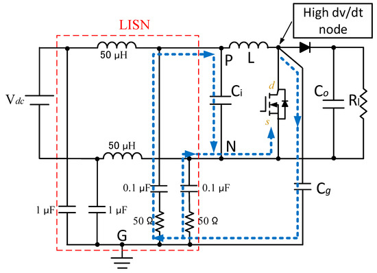
Figure 1.
Configuration of the conventional boost circuit (CBC) and LISN setup.
2.1. Propagation Path of CM Noise Current and the Equivalent Model
At the conducted noise frequency band (from 150 kHz to 30 MHz), the relative impedance of the capacitor is small and the inductor is large. Therefore, Ci (100 μF) and L (500 μH) could be considered as short and open, respectively, in the CM noise model. The conducted noise was generated by the high-frequency voltage fluctuation between the drain and source of the switch. Here in the CBC, the source voltage is almost constant even when the switch is working. On the other hand, as marked as the high dv/dt node in Figure 1, the drain voltage changes rapidly and large CM current flows through Cg to the ground. In conclusion, the blue dotted line in Figure 1 indicates the flow direction of CM current.
The CM noise model resulted from the developed analysis is shown in Figure 2. Here, ZLISN represents the equivalent resistance of LISN, which could be taken as a 25 Ω resistor in CM noise calculation. VN is the noise source, represents the voltage between drain and source of the switch (namely Vds). ZCg is the impedance of Cg. According to the EMI measurement specification, the length of the connecting wire between EUT and LISN should be equal to 80 cm. Here, to improve the accuracy of the noise model, the impedance of the connecting wire is considered and represented as ZW.
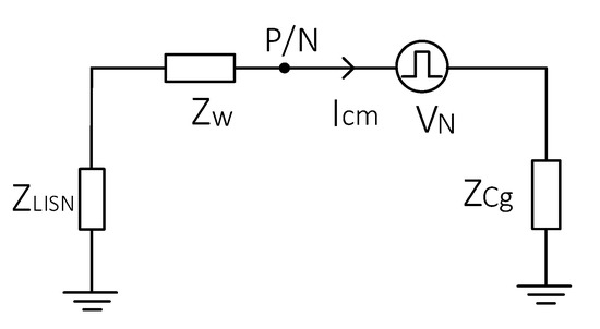
Figure 2.
Common mode (CM) noise model of the conventional boost circuit.
According to the equivalent noise model, the CM noise voltage of CBC could be represented by Equation (1):
This equation is true in both time and frequency domains, and the calculations in this paper are performed in a frequency domain.
2.2. Accurate Noise Source Modeling Method
As mentioned in the introduction, the precision of the noise model is largely affected by the noise source. Thus, plenty of methods have been proposed to obtain the noise source in time or in frequency domain. In this article, a novel frequency domain modeling method is introduced. The computational complexity is reduced while the accuracy is guaranteed. Specifically, the switch voltage waveform during experiment was observed and classified in time domain, and then, the overall spectrum could be obtained in frequency domain by calculating the Fourier series by parts. The accuracy of the noise source model is improved remarkably after considering the high frequency ringing.
The general steps for noise source modeling include:
(1) Capture the turning on and turning off waveforms of the switch by the oscilloscope, while adjusting the appropriate time scale in order to observe the parameters.
(2) Divide the overall waveform into three parts: trapezoid, turn-off ringing, and turn-on ringing. Extract the necessary parameters for the Fourier transform.
(3) Calculate Fourier series of each component separately and then add them together. Finally, the overall spectrum could be obtained.
To specify the modeling process, an experimental setup was established according to Figure 1. Details of the experimental configuration are given in the following section. The key parameters of the circuit are given in Table 1. In addition, 1nF Y-capacitor was adopted as Cg.

Table 1.
Key parameters of CBC.
Figure 3 shows the voltage waveform of switch measured by oscilloscope. The ringing caused by turn-on and turn-off could be seen clearly from the following magnified images. Note that the turn-on ringing is quite limited and thus, its effectiveness could be ignored.
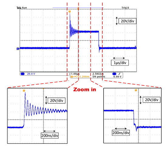
Figure 3.
The experimental voltage waveform of switch measured by oscilloscope.
As the real voltage waveform is an irregular shape, it is difficult to calculate its spectrum directly. This paper decomposed the switch voltage waveform and the Fourier series could be done in steps. The corresponding decomposition process of the overall waveform is shown in Figure 4. The overall waveform is shown at the top of the figure, and it can be divided into the trapezoid component and the ringing component. This decomposition has reduced the complexity of Fourier transformation and improved the precision at the same time. The relative parameters are also marked in Figure 4, which could help to identify the corresponding symbols listed in Table 2.
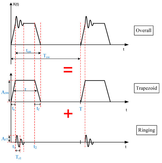
Figure 4.
Decomposition diagram of the switch voltage waveform.
Table 2.
Characteristic parameters of the switch voltage waveform.
According to the mathematical definition [14], the formula for calculating the Fourier series corresponding to trapezoid could be expressed in Equation (2).
In order to approximate the experimental waveform, the difference of turn-on time and turn-off time was also taken into consideration.
Before calculating Fourier series of the ringing waveform, it is better to clarify the corresponding time-domain expressions. The ringing shown in Figure 4 begins after the switch turns off (t1), and will last until the switch turns on (t2). Therefore, it could be written as a piecewise function, as is presented in Equation (3):
According to the definition, the formula for calculating Fourier series can be written as in Equation (4). Then, the Fourier series of the ringing part can be calculated by substituting Equation (3) into Equation (4).
Finally, the Fourier coefficient of the overall switch waveform would be expressed as in Equation (5).
Figure 5 shows the experimental setup for capturing the voltage waveform and measuring the conducted EMI noise. The connection order is the same with configuration in Figure 1. In addition, the spectrum analyzer is connected with LISN to receive and analyze the signal, and the PC is used to display and record the spectra results. The EUT in this article is the conventional boost circuit and the different balanced boost circuits.
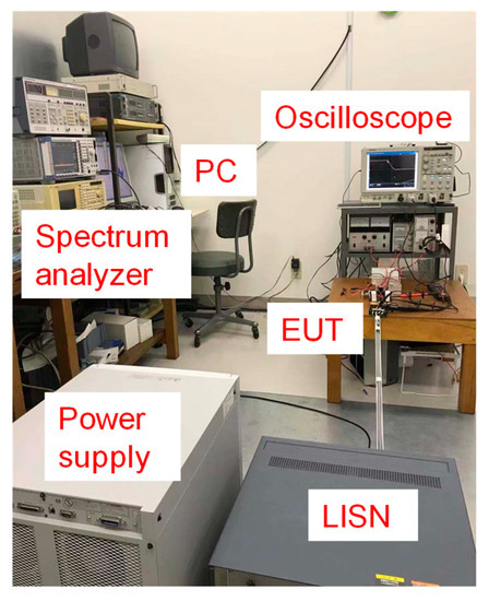
Figure 5.
The experimental setup of conducted noise measurement.
According to Equations (2)–(5) and the measured data, the Fourier series calculation was completed with Matlab 2015b. Figure 6 shows the noise source spectra comparison between experimental and calculation results. The calculation results are plotted in the blue line, and the red experimental results refer to Fast Fourier Transformation (FFT) computed by the oscilloscope. The comparison shows that the calculation results match the experimental result in all frequency ranges. The high-frequency peak is caused by the ringing, and this frequency (around 23.5 MHz) agrees with the frequency of ringing waveform in Figure 3 (Tr1 = 42.3 ns). The effectiveness of this frequency domain modeling method and the obtained parameters was well verified.
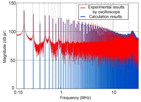
Figure 6.
The frequency spectra of switch voltage (noise source) comparison between calculation and measured results.
Furthermore, based on Equation (1), Figure 7 shows the prediction result of CBC by utilizing the calculated noise source. The experimental result measured by LISN is also given in green. It can be observed that the prediction result matches the measurement in the whole frequency band, and this model is able to predict CM noise with good accuracy.
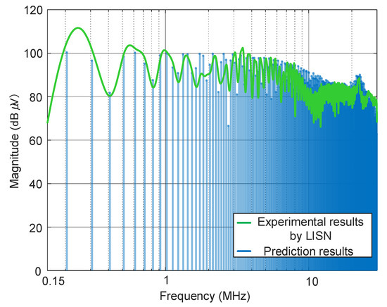
Figure 7.
CM noise spectra comparison of a conventional boost converter (CBC) between prediction and measured results.
3. Analysis and Modeling of Impedance Balancing Technique
Instead of adding conventional passive or active EMI filters, the impedance balancing technique could reduce the conducted noise by changing the topology of CBC. The configuration of balanced boost converter along with LISN is shown in Figure 8. Compared with Figure 1, the power inductor L was split into two parts (L1 and L2) and another capacitor C2 was placed between the N phase and the ground. This action changes the path of the noise current without affecting the efficiency of the circuit.
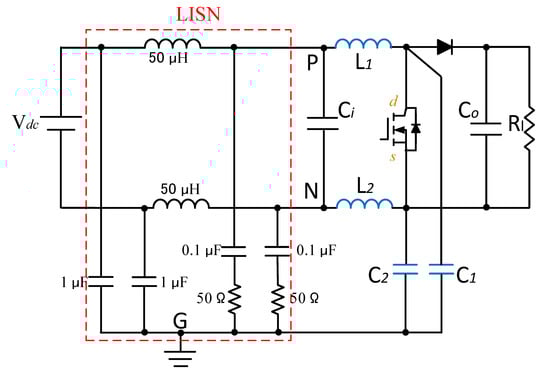
Figure 8.
Configuration of the balanced boost converter and LISN.
3.1. CM Noise Model of Impedance Balanced Boost Circuit
The corresponding CM noise model of balanced boost circuit is shown in Figure 9a. The model includes the equivalent parallel capacitor (EPC) and equivalent parallel resistor (EPR) of each inductor, as well asthe equivalent series inductor (ESL) and equivalent series resistor (ESR) of each capacitor. These parameters may affect the self-resonant frequency and cause impedance unbalancing as well. In addition, a more simplified model obtained according to the Thevenin theorem is shown in Figure 9b.
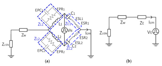
Figure 9.
(a) CM noise model of the impedance balanced boost circuit; (b) simplified CM noise model by the Thevenin theorem.
VE and ZE in the figure are the equivalent noise source and the equivalent impedance, respectively. VN is the same with CBC since the driver circuit of the switch is the same with CBC, and the implement of balancing impedance would not affect the efficiency of the circuit. The relationships between VE, ZE, VN, and the impedance bridge arms are shown in Equations (6) and (7).
where ZL1, ZL2, ZC1 and ZC2 are the impedance of each arm. Furthermore, the voltage of LISN can be expressed as in Equation (8), which has a similar form as Equation (1).
Specifically, no CM current would flow through LISN if the impedance of each bridge arm could satisfy the condition in Equation (9):
where n represents the impedance ratio.
According to the above analysis, the most important step of a balanced circuit is selecting the appropriate impedance arms and keeping the impedance ratio (n) stable during all the target frequency bands. The coupled inductor has been previously used in publications due to its smaller size [19,20,21]. However, unexpected problems have also arisen. Firstly, the coupling coefficient not only affects the inductance value after decoupling but also imposes specific requirements on the selection of core. In [19], the toroidal core has been replaced because it is hard to acquire a high coupling coefficient when the turn ratio is high. Secondly, the parasitic capacitors between the primary side and secondary side make the route of CM noise propagation really complicated. This component has greatly increased the difficulty of modeling analysis and may cause poor reduction results at the same time. Therefore, two isolated inductances were adopted in this paper to prevent these consequences.
In this article, as the power inductor in the CBC is 500 μH, two 250 μH inductors (L1, L2) and two 1nF Y-capacitors (C1, C2) were utilized to build the balanced circuit. The magnitude spectra of impedance bridge arms are shown in Figure 10. The figure shows that both inductors and capacitances are well matched over the frequency range. The condition of balancing impedance is properly satisfied.
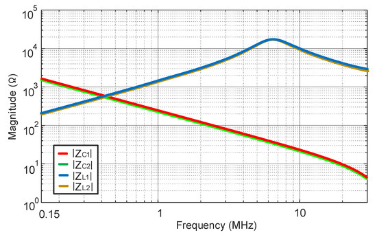
Figure 10.
Magnitude comparison of bridge arms impedance (ZC1 VS. ZC2 and ZL1 VS. ZL2).
Figure 11 shows the experimental CM noise spectrum of balanced boost circuit, which is plotted in red. Meanwhile, the green envelope is the CM noise of CBC (same as in Figure 7). By utilizing the balanced technique, the noise level was well attenuated from 0.5 MHz and upwards. The effect of this technique is obvious, as much as 40 dB reduction was done at some frequency points. Nevertheless, the noise peak at low frequency bands degraded the performance. The relative analysis and solution are given in the following sections.
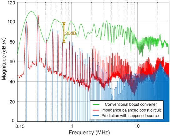
Figure 11.
CM noise spectra comparison of balanced impedance circuit.
3.2. Noise Source Evaluation and Noise Spectrum Prediction
As is shown in Figure 11, the CM noise of balanced boost circuit did not dropped to zero, even if the impedance arms are almost balanced. This means that Equation (7) could not calculate the equivalent noise source accurately. This error may be caused by the interference of the PCB layout and the inevitable mismatch of the impedance. Therefore, this article proposed a novel method to evaluate the attenuation level of the noise source and give prediction accordingly.
Comparing the voltage of LISN in the CBC and the balanced boost circuits, which are represented in Equations (1) and (8), respectively, it should be noted that the two formulas have the same form and the difference is the impedance ZE and ZCg in the denominator. This also means that the first half of Equations (1) and (8) are the same when ZE equals to ZCg, and then the differences of the two noise sources can be directly deducted from the CM noise spectra, as shown in Figure 11.
The equivalent impedance of balanced boost circuit ZE could be calculated by Equations (6), or measured directly. The error between the two results is small. Referring to Equation (6), ZE0 represents the entire impedance of 250 μH inductors (L1, L2) paralleled with 1 nF capacitors (C1, C2). Figure 12 shows the impedance variation of ZCg and ZE0 through frequency. The ZCg is larger than ZE0 from 0.15 MHz to 0.69 MHz, and then the ZE0 becomes larger from 0.69 MHz.
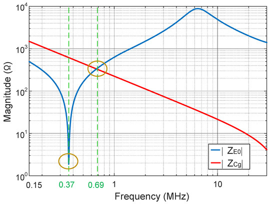
Figure 12.
Magnitude spectra comparison between ZE0 (250 μH and 1 nF) and ZCg.
According to Figure 12, it should be noted that ZCg equals ZE0 at the point of 0.69 MHz, where the noise of balanced circuit is 80 dBμV and the CBC is about 100 dBμV. This spectra difference equals to 20 dBμV, which means that VN is about 10 times of VE according to the definition. Therefore, this paper assumed that VE is one-tenth of VN and then substituted other measured impedance values into Equations (8) for calculation.
The prediction results are plotted in translucent blue in Figure 11 and are basically consistent with the measured spectrum except for the medium frequency band. This comparison confirms the hypothesis.
In addition, the resonance frequency of impedance arms could be calculated by Equations (10).
Specially, when L1 and L2 equal to 250 μH, C1 and C2 equal to 1nF, the series resonance of ZE0 happens at 0.37 MHz, which agrees with the noise peak in Figure 10. Therefore, it is necessary to find corresponding countermeasures to optimize the known impedance balancing technique.
4. Optimized Schemes with Redesigned Impedance Arms
As shown in Figure 11, the noise peak occurs at the resonant frequency; thus, several researchers have proposed different methods to solve the spike problem. In [17], the authors changed the inductance value and added a pF-class capacitor to cooperate with the impedance ratio in Equation (9). However, this may push the noise spike to the middle or high frequency band. The designing method of the inductor in [21] achieved satisfactory results, but this result is based on an additional CM choke filter. As opposed to previous methods, this paper adjusted the values of passive elements to move the resonance peak out of the conductive frequency range.
As was mentioned in the previous section, a low-frequency peak occurs because of the series resonance among the four impedance bridge arms. On the other hand, it is hard to further suppress the equivalent noise source because the impedance arms are well matched, especially at a low frequency. Thus, the more practical method is to redesign the value of inductors or capacitors. Without changing the balancing configuration shown in Figure 8. This paper has proposed two alternative schemes to attenuate the noise peak according to Equations (10). One is increasing the inductor to 1.4 mH and the other is increasing the value of Y-capacitors to 4.7 nF. The following sections will investigate and compare the two approaches.
4.1. Balanced Boost Circuit with 1.4 mH Inductors and 1 nF Y-capacitors
After calculation using Equations (10), the inductance should be larger than 1.3 mH if the capacitors C1 and C2 are kept constant. Here, two1.4mH inductors were utilized to replace the 250 μH inductors. The experimental results were recorded and drawn with black in Figure 13, compared with the former balanced boost circuit in red and the green envelope of CBC. These experimental results show that the proposed balanced scheme with 1.4 mH inductors and 1nF capacitors could attenuate noise level over all frequency range compared with CBC. Furthermore, the spike at 0.37 MHz was effectively suppressed. However, the noise at high frequency increased in contrast with the former balanced boost circuit (250 μH and 1 nF). The valley at 0.8 MHz is due to the self-resonance between the 1.4 mH inductor and its EPCs.
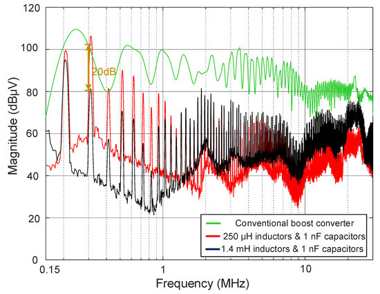
Figure 13.
CM noise comparison after replacing the 250 μH inductors with 1.4 mH inductors.
Referring to Equations (6), ZE1 identifies the whole impedance including 1.4 mH inductors and 1nF Y-capacitors. Figure 14 gives its magnitude in black and makes comparison with ZCg in red. Note that ZE1 equals to ZCg at 0.24 MHz, which means that the noise source attenuation degree could be speculated quickly With the same analysis method as the one in Section 3. According to Figure 13, the noise spectra difference around 0.24 MHz reached about 20 dBμV, which indicates that the equivalent noise source VE in the optimized scheme was attenuated well compared with CBC. However, a drawback of this approach is the increased weight and volume of the circuit.
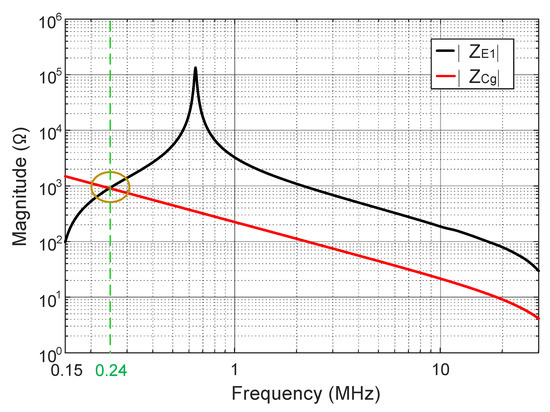
Figure 14.
Impedance comparison between ZE1 (1.4 mH and 1 nF) and ZCg.
4.2. Balanced Boost Circuit with 250 μH Inductors and 4.7 nF Y-capacitors
Other than using a pair of larger inductors, this scheme utilized greater Y-capacitors to decrease the series resonant frequency. After calculation, 4.7 nF capacitors were selected to replace the former 1nF capacitors and the other experimental conditions were kept the same.
The CM noise spectra comparison is shown in Figure 15. The purple curve is for the case of an optimized solution after replacing the 1 nF Y-capacitors with 4.7 nF, the green one is the noise envelope of CBC, and the red one is for the former balanced circuit boost (250 μH and 1 nF). The comparison shows that after utilizing the scheme with 4.7 nF capacitors, a low-frequency spike was also moved out from the frequency band of interest and the CM noise was significantly attenuated. Meanwhile, at a high frequency, the noise after adopting 4.7 nF capacitors is lower than the former case using 1 nF capacitors.
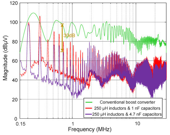
Figure 15.
CM noise comparison after replacing the 1 nF Y-capacitors with 4.7 nF Y-capacitors.
Similarly to ZE1, ZE2 represents the whole bridge impedance of 250 μH inductors and 4.7 nF Y-capacitors. The comparison between ZE2 (purple) and ZCg (red) is shown in Figure 16. The resonant frequency of optimized impedance ZE2 was removed to around 0.16 MHz and the performance at high frequency is almost the same compared to that in Figure 12. At 0.68 MHz, where ZE2 equals ZCg, about 30 dB reduction was achieved according to Figure 15. Compared with the former balanced boost circuit (250 μH and 1 nF), the noise source was significantly attenuated and the performance was improved over the entire frequency range.
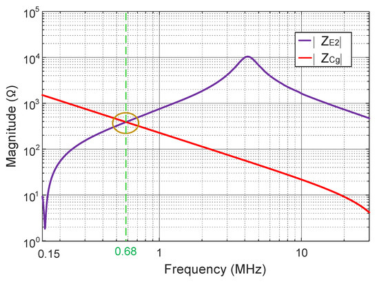
Figure 16.
Impedance comparison between ZE2 (250 μH and 4.7 nF) and ZCg.
There may be some concerns that the greater capacitor may increase the CM current and exceed relative standards. Figure 17 shows the CM currents comparison between CBC and the optimized balanced boost circuit (250 μH and 4.7 nF). The results show that with optimized schemes, the CM current becomes even smaller because the noise source has been effectively attenuated.
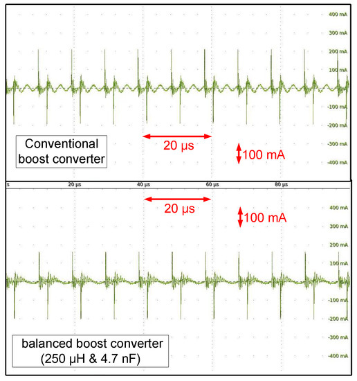
Figure 17.
Experimental CM current waveforms comparison between CBC and optimized impedance balancing boost converter (250 μH and 4.7 nF).
In summary, the optimized scheme of changing the capacitors is more effective than replacing the inductors, which not only considers the attenuation results but also the cost and the difficulty of implementation.
A comparative investigation between the proposed work and the previously published relevant arts was carried out and is addressed in Table 3. The comparison reveals the effectiveness and practicability of the proposed schemes.
Table 3.
Comparison of noise optimization effects.
5. Conclusions
Focusing on the noise attenuation with impedance balancing technique, a frequency domain modeling method and two optimized schemes are introduced in this paper. The accurate noise source model was extracted by capturing the switch voltage waveform and then calculating its Fourier series. Furthermore, for both noise source and CM noise of the conventional boost circuit, the accuracy of the noise model were verified by comparing the prediction results with the experimental measurements.
Then, the impedance balancing technique was adopted to attenuate the noise. Although this technique is effective to some extent, it suffers from noise spikes and also lacks a model that can predict the noise quantitatively. In this research, the noise source attenuation degree was evaluated by combining the noise spectra and impedance information. Furthermore, a quantitative prediction based on the proposed noise model is provided. A comparison between prediction and experimental results was conducted and the accuracy of the proposed noise model was practically verified.
Based on the basic impedance balancing configuration and the calculation formula of resonance frequency, two optimized schemes were proposed to deal with the noise peak in the low-frequency band. The size of the impedance arms was redesigned and the two schemes were investigated in different aspects. Finally, the experimental results were presented to demonstrate the analysis. The contribution of this research is enhancing the feasibility and effectiveness of the known impedance balancing technique.
Author Contributions
Conceptualization, methodology, investigation, S.Z., B.Z., M.S., and G.M.D.; validation, S.Z. and Q.L.; writing—review and editing S.Z. and G.M.D.; supervision M.S. and G.M.D.; project administration, E.T. All authors have read and agreed to the published version of the manuscript.
Funding
This research received no external funding.
Conflicts of Interest
The authors declare no conflict of interest.
References
- Mainali, K.; Oruganti, R. Conducted EMI Mitigation Techniques for Switch-Mode Power Converters: A Survey. IEEE Trans. Power Electron. 2010, 25, 2344–2356. [Google Scholar] [CrossRef]
- Tarateeraseth, V.; Hu, B.; See, K.Y.; Canavero, F.G. Accurate Extraction of Noise Source Impedance of an SMPS Under Operating Conditions. IEEE Trans. Power Electron. 2010, 25, 111–117. [Google Scholar] [CrossRef]
- Yang, L.; Lu, B.; Dong, W.; Lu, Z.; Xu, M.; Lee, F.C.; Odendaal, W.G. Modeling and characterization of a 1 KW CCM PFC converter for conducted EMI prediction. In Proceedings of the Nineteenth Annual IEEE Applied Power Electronics Conference and Exposition, APEC’04, Anaheim, CA, USA, 22–26 February 2004; Volume 2, pp. 763–769. [Google Scholar]
- Lai, J.; Huang, X.; Pepa, E.; Chen, S.; Nehl, T.W. Inverter EMI modeling and simulation methodologies. IEEE Trans. Ind. Electron. 2006, 53, 736–744. [Google Scholar]
- Gubia, E.; Sanchis, P.; Ursua, A.; Lopez, J.; Marroyo, L. Frequency domain model of conducted EMI in electrical drives. IEEE Power Electron. Lett. 2005, 3, 45–49. [Google Scholar] [CrossRef]
- Pei, X.; Zhang, K.; Kang, Y.; Chen, J. Prediction of common mode conducted EMI in single phase PWM inverter. In Proceedings of the 2004 IEEE 35th Annual Power Electronics Specialists Conference (IEEE Cat. No.04CH37551), Aachen, Germany, 20–25 June 2004; Volume 4, pp. 3060–3065. [Google Scholar]
- Liu, Q.; Wang, F.; Boroyevich, D. Modular-Terminal-Behavioral (MTB) Model for Characterizing Switching Module Conducted EMI Generation in Converter Systems. IEEE Trans. Power Electron. 2006, 21, 1804–1814. [Google Scholar]
- Bishnoi, H.; Mattavelli, P.; Burgos, R.; Boroyevich, D. EMI Behavioral Models of DC-Fed Three-Phase Motor Drive Systems. IEEE Trans. Power Electron. 2014, 29, 4633–4645. [Google Scholar] [CrossRef]
- Kerrouche, B.; Bensetti, M.; Zaoui, A. New EMI Model with the Same Input Impedances as Converter. IEEE Trans. Electromagn. Compat. 2019, 61, 1072–1081. [Google Scholar] [CrossRef]
- Mainali, K.; Oruganti, R. Simple Analytical Models to Predict Conducted EMI Noise in a Power Electronic Converter. In Proceedings of the IECON 2007—33rd Annual Conference of the IEEE Industrial Electronics Society, Taipei, Taiwan, 5–8 November 2007; pp. 1930–1936. [Google Scholar]
- Jin, M.; Weiming, M. Power Converter EMI Analysis Including IGBT Nonlinear Switching Transient Model. IEEE Trans. Ind. Electron. 2006, 53, 1577–1583. [Google Scholar] [CrossRef]
- Xia, Y.; Gu, Y.; Shen, J. Conducted EMC Modeling for EV Drives Considering Switching Dynamics and Frequency Dispersion. In Proceedings of the 2018 IEEE Energy Conversion Congress and Exposition (ECCE), Portland, OR, USA, 23–27 September 2018; pp. 4195–4202. [Google Scholar]
- Xiang, Y.; Pei, X.; Zhou, W.; Kang, Y.; Wang, H. A Fast and Precise Method for Modeling EMI Source in Two-Level Three-Phase Converter. IEEE Trans. Power Electron. 2019, 34, 10650–10664. [Google Scholar] [CrossRef]
- Zhang, B.; Zhang, S.; Li, H.; Shoyama, M.; Takegami, E. An Improved Simple EMI Modeling Method for Conducted Common Mode Noise Prediction in DC-DC Buck Converter. In Proceedings of the IEEE ICDCM’19, Matsue, Japan, 20–23 May 2019; pp. 1–6. [Google Scholar]
- Kim, T.; Feng, D.; Jang, M.; Agelidis, V.G. Common Mode Noise Analysis for Cascaded Boost Converter with Silicon Carbide Devices. IEEE Trans. Power Electron. 2017, 32, 1917–1926. [Google Scholar] [CrossRef]
- Shoyama, M.; Li, G.; Ninomiya, T. Balanced switching converter to reduce common-mode conducted noise. IEEE Trans. Ind. Electron. 2003, 50, 1095–1099. [Google Scholar] [CrossRef]
- Wang, S.; Kong, P.; Lee, F.C. Common Mode Noise Reduction for Boost Converters Using General Balance Technique. IEEE Trans. Power Electron. 2007, 22, 1410–1416. [Google Scholar] [CrossRef]
- Xing, L.; Sun, J. Conducted Common-Mode EMI Reduction by Impedance Balancing. IEEE Trans. Power Electron. 2012, 27, 1084–1089. [Google Scholar] [CrossRef]
- Kong, P.; Wang, S.; Lee, F.C. Improving balance technique for high frequency common mode noise reduction in boost PFC converters. In Proceedings of the 2008 IEEE Power Electronics Specialists Conference, Rhodes, Greece, 15–19 June 2008; pp. 2941–2947. [Google Scholar]
- Kong, P.; Wang, S.; Lee, F.C. Common Mode EMI Noise Suppression for Bridgeless PFC Converters. IEEE Trans. Power Electron. 2008, 23, 291–297. [Google Scholar] [CrossRef]
- Zhang, Y.; Zheng, F.; Wang, Y. Alleviation of Electromagnetic Interference Noise Using a Resonant Shunt for Balanced Converters. IEEE Trans. Power Electron. 2015, 30, 4762–4773. [Google Scholar] [CrossRef]
© 2020 by the authors. Licensee MDPI, Basel, Switzerland. This article is an open access article distributed under the terms and conditions of the Creative Commons Attribution (CC BY) license (http://creativecommons.org/licenses/by/4.0/).