A Four-Channel CMOS Front-End for Interference-Robust GNSS Receiver


Abstract
1. Introduction
2. System Architecture
3. Circuit Implementations
3.1. LNA
3.2. Mixer
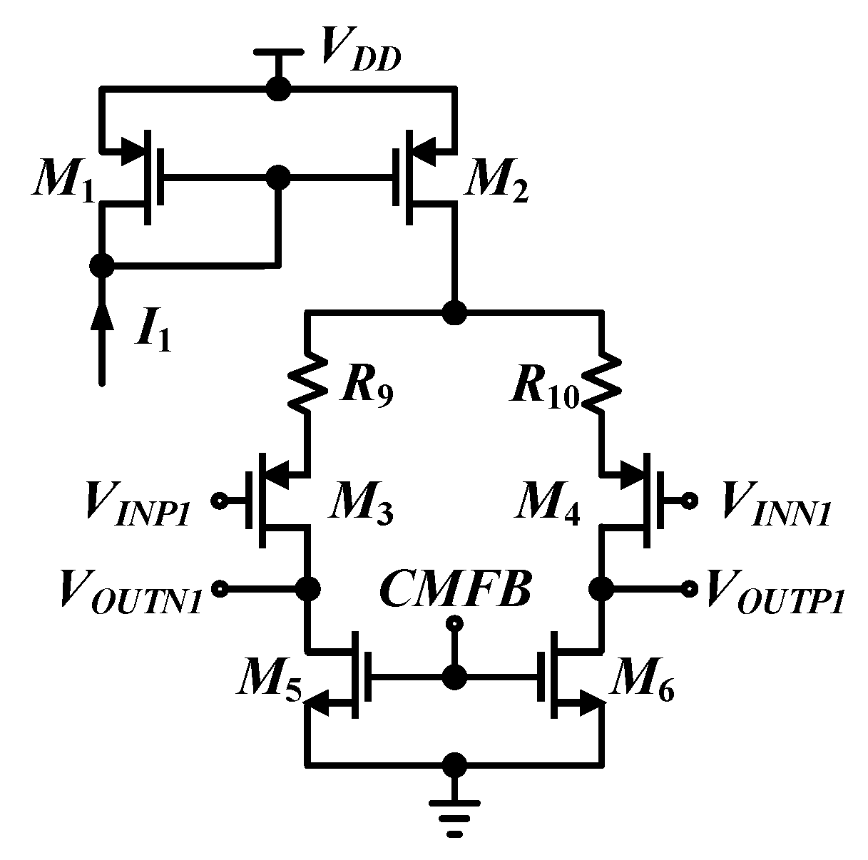
3.3. IFA
3.4. PLL
4. Measurement Results
5. Conclusions
Author Contributions
Funding
Conflicts of Interest
References
- Braasch, M.S.; Van Dierendonck, A.J. GPS receiver architectures and measurements. Proc. IEEE 1999, 87, 48–64. [Google Scholar] [CrossRef]
- Wang, Y.; Gao, B.; Li, P.; Ni, X.; Zhou, R. A RF CMOS GNSS receiver with a passive mixer for GPS L1/Galileo E1/Compass B1 band. IEICE Electron. Express 2018, 15-20180551. [Google Scholar] [CrossRef]
- Valle De Lima, D.; Da Costa, J.P.C.L.; Maranhao, J.P.A.; de Sousa, R.T. Time-delay estimation via procrustes estimation and Khatri-Rao factorization for GNSS multipath mitigation. In Proceedings of the 2017 11th International Conference on Signal Processing and Communication Systems (ICSPCS), Gold Coast, Australia, 13–15 December 2017; pp. 1–7. [Google Scholar] [CrossRef]
- Schafer, E.; Irteza, S.; Jager, A.; Bieske, B.; Richter, A.; Khan, M.A.; Sathyamurthy, M.; Kerkmann, S.; Rolapp, A.; Hennig, E.; et al. A four-channel GNSS front-end IC for a compact interference- and jamming-robust multi-antenna Galileo/GPS receiver. In Proceedings of the 2014 7th ESA Workshop on Satellite Navigation Technologies and European Workshop on GNSS Signals and Signal Processing (NAVITEC), Noordwijk, The Netherlands, 3–5 December 2014; pp. 1–6. [Google Scholar] [CrossRef]
- Konovaltsev, A.; Antreich, F.; Hornbostel, A. Performance assessment of antenna array algorithms for multipath and interferers mitigation. In Proceedings of the 2007 GNSS Signals and Signal Processing Workshop, Noordwijk, The Netherlands, 24–25 April 2007; pp. 24–25. [Google Scholar]
- Chen, D.; Pan, W.; Jiang, P.; Jin, J.; Mo, T.; Zhou, J. Reconfigurable dual-channel multiband RF receiver for GPS/Galileo/BD-2 systems. IEEE Tran. Microw. Theory Tech. 2012, 60, 3491–3501. [Google Scholar] [CrossRef]
- Wu, J.; Jiang, P.; Chen, D.; Zhou, J. A dual-band GNSS RF front end with a pseudo-differential LNA. IEEE Trans. Circuits Syst. II Exp. Briefs 2011, 58, 134–138. [Google Scholar] [CrossRef]
- Li, S.; Li, J.; Gu, X.; Wang, H.; Li, C.; Wu, J.; Tang, M. Reconfigurable all-band RF CMOS transceiver for GPS/GLONASS/Galileo/Beidou with digitally assisted calibration. IEEE Trans. Very Large Scale Integr. (VLSI) Syst. 2014, 23, 1814–1827. [Google Scholar] [CrossRef]
- Steyaert, M.; Coppejans, P.; De Cock, W.; Leroux, P.; Vancorenland, P. A fully-integrated GPS receiver front-end with 40mW power consumption. In Proceedings of the 2002 IEEE International Solid-State Circuits Conference. Digest of Technical Papers (ISSCC), San Francisco, CA, USA, 7 February 2002; pp. 320–528. [Google Scholar] [CrossRef]
- Galileo OS SIS ICD. Available online: https://www.gsc-europa.eu/sites/default/files/sites/all/files/Galileo-OS-SIS-ICD.pdf (accessed on 1 December 2016).
- General Specification for BDS/GNSS RTK Receiver. Available online: http://m.beidou.gov.cn/zt/bdbz/201911/W020191125788479580570.pdf (accessed on 1 December 2019).
- Kim, T.W.; Kim, B.; Lee, K. Highly linear receiver front-end adopting MOSFET transconductance linearization by multiple gated transistors. IEEE J. Solid-State Circuits 2004, 39, 223–229. [Google Scholar] [CrossRef]
- Gao, W.; Chen, Z.; Liu, Z.; Cui, W.; Gui, X. A highly linear low noise amplifier with wide range derivative superposition method. IEEE Microw. Wirel. Compon. Lett. 2015, 25, 817–819. [Google Scholar] [CrossRef]
- Shahani, A.R.; Shaeffer, D.K.; Lee, T.H. A 12-mW wide dynamic range CMOS front-end for a portable GPS receiver. IEEE J. Solid-State Circuits 1997, 32, 2061–2070. [Google Scholar] [CrossRef]
- Zhao, M.; Liao, J. A compact low power current-mode LNA-Mixer for RF receiver. IEICE Electron. Express 2017, 14, 20170773. [Google Scholar] [CrossRef][Green Version]
- Kianpour, I.; Hussain, B.; Tavares, V.G.; Mendonça, H.S. A low-power multi-tanh OTA with very low harmonic distortion. In Proceedings of the 2015 IEEE International Symposium on Circuits and Systems (ISCAS), Lisbon, Portugal, 24–27 May 2015; pp. 645–649. [Google Scholar] [CrossRef]
- Liscidini, A.; Mazzanti, A.; Tonietto, R.; Vandi, L.; Andreani, P.; Castello, R. Single-stage low-power quadrature RF receiver front-end: The LMV cell. IEEE J. Solid-State Circuits 2006, 41, 2832–2841. [Google Scholar] [CrossRef]
- Heiberg, A.C.; Brown, T.W.; Fiez, T.S.; Mayaram, K. A 250 mV, 352μW GPS Receiver RF Front-End in 130 nm CMOS. IEEE J. Solid-State Circuits 2011, 46, 938–949. [Google Scholar] [CrossRef]


| This Work | [4] | [6] | [17] | [18] | |||
|---|---|---|---|---|---|---|---|
| Process (nm) | 180 | 180 | 180 | 130 | 130 | ||
| Number of Channels | 4 | 4 | 2 | 1 | 1 | ||
| Frequency (GHz) | 1.2 | 1.57 | 1.2/1.57 | 1.57 | 1.575 | ||
| Supply (V) | 1.8/3.3 | 1.8/3.3 | 1.8 | 1.2 | 0.25 | 0.3 | 0.4 |
| Gain (dB) | 40 * | 83 | 110 * | 36 * | 41.8 | 42.2 | 42.5 |
| P-1dB (dBm) | −18 | −73.5 | −42/−39 | −31 | −48 | −47 | −45.7 |
| IIP3 (dBm) | −8 | − | − | −19 | −35.8 | −35.2 | −34 |
| Phase noise at 1 MHz (dBc/Hz) | −126.26 | −107 | −122/−124 | −104 | −112.4 | −112.5 | −113.8 |
| S11 (dB) | −16 | − | −13/−12 | <−10 | <−10 | ||
| JSR (dB) | 72 | 45 | − | − | − | ||
| Area (mm2) | 20 | 25 | 2.4 | 1.5 | 5.76 | ||
© 2020 by the authors. Licensee MDPI, Basel, Switzerland. This article is an open access article distributed under the terms and conditions of the Creative Commons Attribution (CC BY) license (http://creativecommons.org/licenses/by/4.0/).
Share and Cite
Han, F.; Gao, J.; Li, X.; Chen, Z. A Four-Channel CMOS Front-End for Interference-Robust GNSS Receiver. Electronics 2020, 9, 291. https://doi.org/10.3390/electronics9020291
Han F, Gao J, Li X, Chen Z. A Four-Channel CMOS Front-End for Interference-Robust GNSS Receiver. Electronics. 2020; 9(2):291. https://doi.org/10.3390/electronics9020291
Chicago/Turabian StyleHan, Fang, Jian Gao, Xiaoran Li, and Zhiming Chen. 2020. "A Four-Channel CMOS Front-End for Interference-Robust GNSS Receiver" Electronics 9, no. 2: 291. https://doi.org/10.3390/electronics9020291
APA StyleHan, F., Gao, J., Li, X., & Chen, Z. (2020). A Four-Channel CMOS Front-End for Interference-Robust GNSS Receiver. Electronics, 9(2), 291. https://doi.org/10.3390/electronics9020291