1. Introduction
Bidirectional direct current-direct current (DC-DC) converters are widely employed in various applications such as renewable energy, battery chargers of electric vehicles (EVs), DC micro-grids and other battery energy storage system (BESS) applications. Typically, to achieve soft switching with superior electro-magnetic interference (EMI) considerations, these converters are implemented based on resonant converters [
1,
2,
3,
4]. This kind of converters have different topologies with respect to their power ratings, voltage levels and input or output required voltage (current) source models. Among them, series resonant converters (SRCs) are the most resilient and practical topologies, which have various control methods, reduced numbers of passive elements and improved efficiency. Moreover, SRCs are more compatible with BESS due to their intrinsic voltage source behavior [
3,
4,
5,
6,
7].
For high power applications such as fast charging of EVs, a dual-active bridge SRC (DAB-SRC) is the well-known structure for the bidirectional power flow control at EV charging infrastructures [
4,
5,
6,
7].
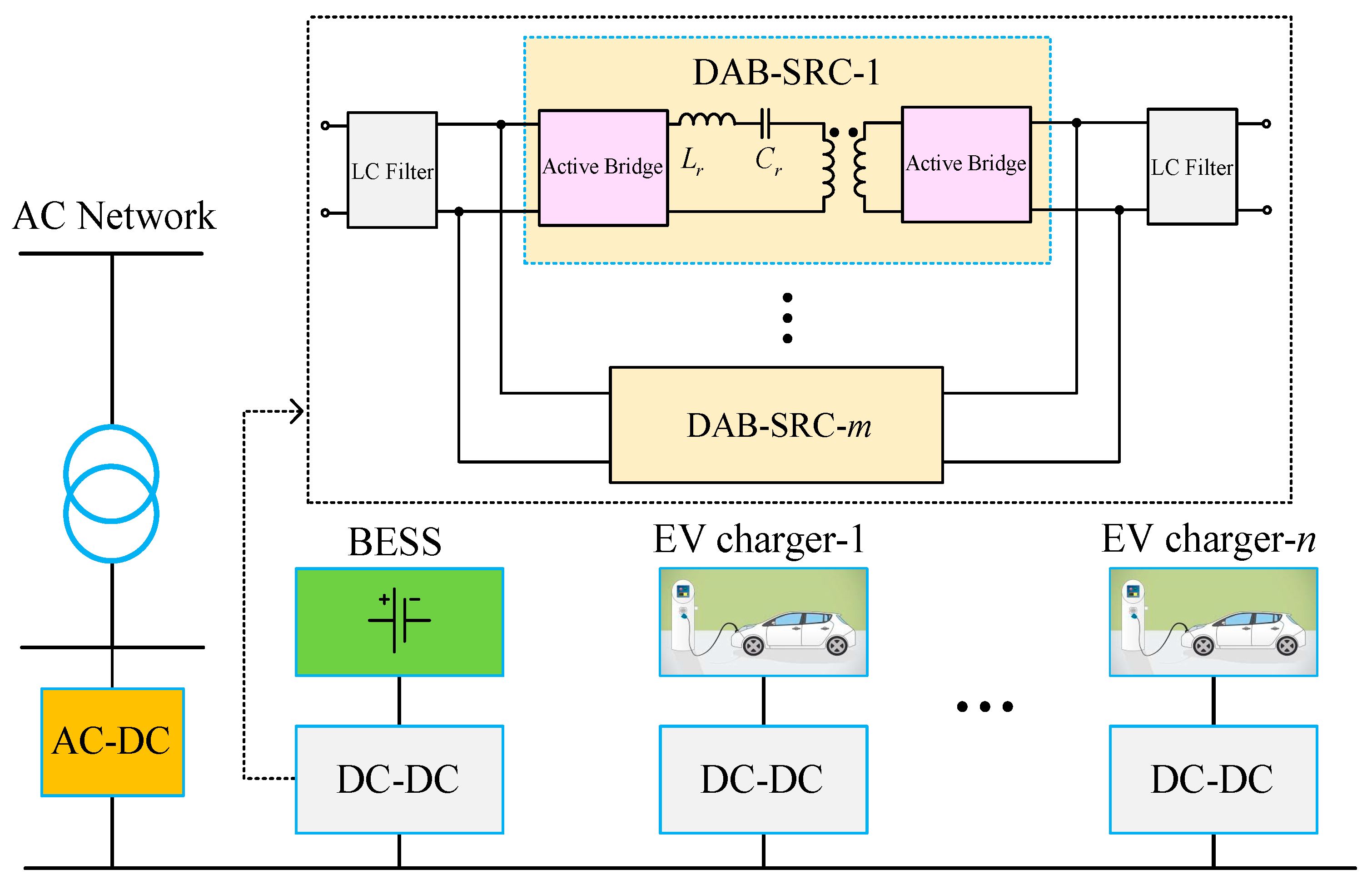
Figure 1 shows a charging stage of EVs based on DAB-SRCs to achieve bidirectional power flow capability between the grid and the electric vehicle, i.e., V2G capability [
8,
9,
10]. Another advantage of DAB-SRC is that it can be implemented in a modular structure without the need for extra input or output filters, as shown in
Figure 1.
The most important problems associated with the state-of-the-art are the power and frequency tuning of these power converters with minimum phase displacement or circulating current [
7,
10,
11,
12]. Current researches are mainly based on algorithms which utilize phase-locked loop (PLL) techniques. PLLs are well-known techniques to tune the switching frequency of resonant converters; however, they are sensitive to uncertainty and tolerances in resonant tank circuits [
3]. Due to high power rating of fast DC chargers, about 100–200 kW, robustness and ability to cope with deviations or tolerances in a resonant tank are essential [
13].
To address this problem, a self-tuning method is proposed which has fast dynamics and is not sensitive to the tolerances. Recently, this method has been utilized for power and frequency tuning of wireless charging of EVs using inductive power transfer (IPT) technology, DC-DC converters and various battery chargers [
3,
14,
15,
16,
17]. Moreover, in self-tuning methods, all the switching methods such as pulse width modulation (PWM), pulse density modulation (PDM) and the phase-shift control method can be implemented. However, in the available researches, the bidirectional capability of the SRCs is not considered in the self-tuning method. Moreover, the formulations and analysis of the self-tuning are derived for an ohmic load [
14,
15,
16,
17].
In this paper, design considerations of the DAB-SRC such as DC-link voltages, bandwidth of the switching frequency, the minimum and maximum of the transferred power and the time displacement between the two active bridges are derived based on the self-tuning loop’s parameters. In addition, a simple control method is proposed which can change the direction of the output power with less transients and power fluctuations. Another advantage is direct control of the phase displacement between the dual active bridges hence; the minimum phase displacement can be achieved simply, which is essential for a DAB-SRC [
11,
12].
As presented in [
16], the proposed method can be implemented based on phase shift and PWM modulations which is essential for DAB-SRCs with different DC-link voltages. However, for the sake of simplicity, the power and frequency tuning is devised based on phase shift controlling between the two active bridges which is a usual solution for approximately equal DC-link voltages [
7].
The rest of this paper is organized as follows: a description of DAB-SRC with and its mathematical model are presented in
Section 2.
Section 3 presents modeling and formulation of the proposed tuning loop for the DAB-SRC.
Section 4 presents simulation results and modification of the analysis to verify the proposed control method in the transient and steady-state conditions and the main conclusions of the paper are summarized in
Section 5.
2. Modeling of a Dual-Active Bridge Series Resonant Converter (DAB-SRC)
In this section, the principle of operation for a DAB-SRC is set forth as follows.
Figure 2 shows the two active bridges with
DC-link voltage of
Vin for the charger side and
VBatt for the EV side as the battery voltage level. In this figure, for simplicity, the input/output filters are not considered and a high-frequency transformer (HFT) is utilized for isolation and better impedance matching between these two sides. In the proposed tuning loop, a current transformer (CT) is used for the resonant tank current sensing,
io, while
Io represents phasor state of
io.
Two simple first order phase shifters are considered for phase displacement between the two bridges, while the Micro-Controller Unit (MCU) can digitally implement these two phase shifters in the discrete time mode. The active bridge that is supposed to send the power is responsible to regulate the power, hence only the leading phase shifter is considered variable. By digital implementation, the system will be more compact and less sensitive to tolerances occurring in the phase shifter circuits. For analog implementation, the variable leading phase shifter resistor,
RT1, can be implemented using a digital-potentiometer or combination of a light-emitting diode and light-dependent resistor (LED-LDR) as discussed in [
17]. In this implementation, the digital-potentiometer or light of LED can be controlled directly from the MCU [
17].
In this paper, the two bridges are switching with duty cycle of about 50%, i.e., neglecting the dead time,
td, between the low side and high side switches. Hence, the two bridges can be considered as two square wave voltage sources connected together by the series resonant tank, i.e., resonant inductor,
Lr and resonant capacitor,
Cr. Using fundamental components, each square voltage source can be modeled as a sinusoidal voltage source as shown in
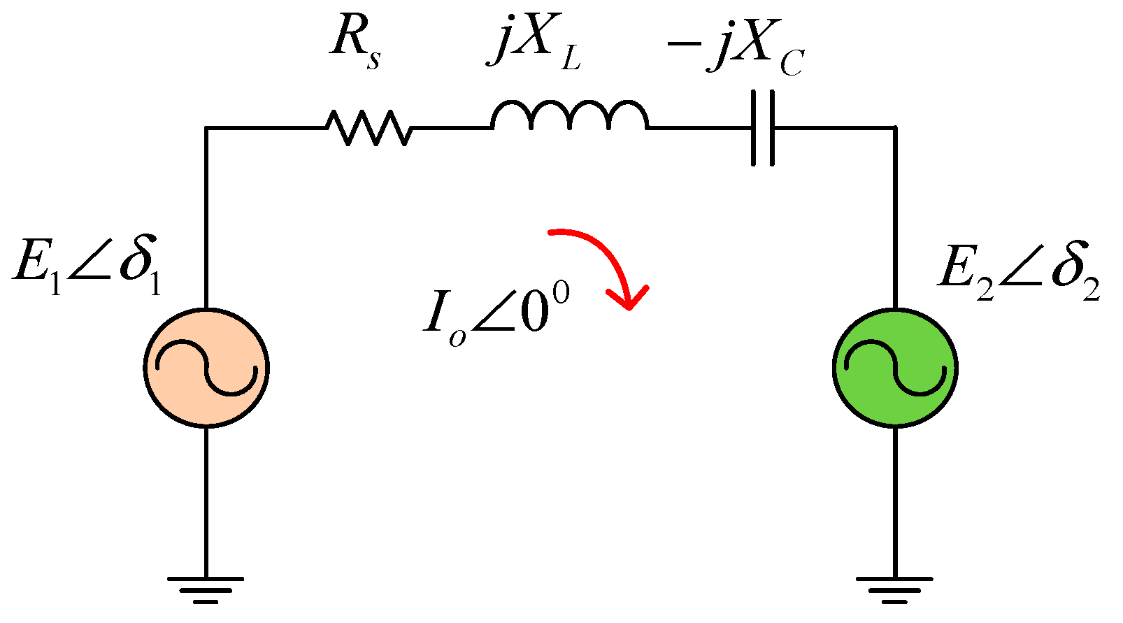
Figure 3. In this Figure,
Rs is the winding resistance of the HFT and
Io is considered as the reference phasor.
E1 and
E2 represent fundamental harmonics of the output voltage of the charger side and EV side referred to the primary side of the HFT, while
e1 and
e2 represent their instantaneous state, respectively. Moreover,
δ1 and
δ2 are phase angles of the aforementioned sinusoidal voltages with respect to the reference phasor, i.e.,
Io. Hence, for the forward power transfer, battery charging, and considering zero voltage switching (ZVS) for the two active bridges, the phase angles must be derived as
δ1 > 0 and
δ2 < 0. This rule is reversed when the battery sends its energy back to the station side while ZVS is achieved [
6,
7,
8,
9,
10]. In the following equations, each phasor is considered based on its maximum value.
E1,
E2 and the natural angular frequency of the power converter are derived by the following equations according to the system parameters:
The impedances presented in
Figure 3 and the equivalent impedance,
Xt, between these two bridges neglecting the series resistor,
Rs ≈ 0, are defined as follows:
where,
ωs is the angular switching frequency. Regarding
Figure 3 and
Rs ≈ 0, the power-angle equation is derived as follow in the forward power direction, i.e., the battery is charging [
7].
Regarding (5), there are different strategies for power flow regulation which are the frequency control, phase control or combination of them [
4,
5,
6,
7,
8,
9,
10]. Using frequency control,
Xt changes to regulate the power while phase control has direct effect on the two phase angles,
δ1 and
δ2. The relation between
E1,
E2 and
Io, is derived by (6), considering
Rs ≈ 0. Hence, the relation between angles and amplitude of the input and output voltages are derived by (7b).
Moreover, the relation between amplitude of resonant tank current, angles and voltage amplitudes are derived as:
To achieve ZVS, the snubber capacitors,
Cs, of the power switches should be considered. Hence, a minimum required phase displacement for each active bridge is defined for the worst case, the minimum current or light load conditions. For the charger and the battery side bridges, the minimum phase displacements for the active bridges with respect to the minimum resonant tank current
Iomin are derived by (9) and (10), respectively, to assure ZVS for the two active bridges. Equations (9) and (10) are derived assuming that the resonant inductor is large enough to keep the current constant at the dead time,
td, of switching.
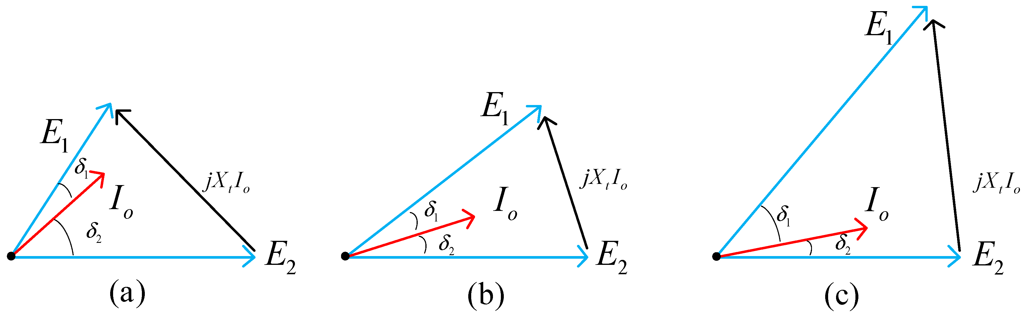
For DAB-SRC there are six possible conditions regarding voltage ratio of the two DC-link sides and three possible conditions are depicted in
Figure 4 in the forward power flow, the battery is charging. Regarding
Figure 4, the equivalent impedance is considered as a pure inductive, meaning that
Rs ≈ 0 and
ωs >
ωn. For
Figure 4a,c, the corresponding phase angle of the lower voltage is significantly derived from the lower rather than the other side phase angle. Hence, in these conditions the lower angle should be considered at the minimum required phase angle for ZVS even for full load condition. This fact is essential for minimum phase displacement achieving and reducing the circulation current. This approach requires precise controlling methods which are depend on system parameters identification.
Another fact is that for unequal voltages, the system requires higher operating frequencies to assure ZVS condition due to large phase difference between the two bridges. In this condition, the wave forms are far from a sinusoidal equation, also achieving ZVS is more difficult for the lower voltage active bridge.
Figure 4b is an idea condition for DAB-SRCs by achieving an equal phase displacement for the two bridges and intrinsic ZVS for simply operating frequencies higher than the natural frequency of the system. This condition
E1 ≈
E2 is proposed for high power application and power and frequency control methods can be applied simply. Moreover, in this condition, the operating frequency can be selected near the natural frequency to achieve almost pure sinusoidal waveforms to reduce power losses in the HFT.
Regardless of the three possible conditions and their corresponding applications, previous research required complex control methods for power and frequency-tuning methods which mainly depend on parameters of the DAB-SRC [
7]. These control methods are sensitive to possible system tolerances. Moreover, systems that are based on PLLs have transients to achieve ZVS which imposes extra EMI at transient conditions and is not recommended for high power applications.
In the next section, the proposed tuning loop is devised based on self-oscillating methods presented in [
17] and the main formulation of the system is derived based on DAB-SRC. The new tuning method can simply assure ZVS condition, regardless of system tolerances. Moreover, the tuning loop has fast dynamics in start-up and power direction changing.
3. Modeling of the Proposed Tuning Loop
Similar to the other self-tuning methods for voltage source inverters [
3], the switching signals are generated by the series resonant load current,
io, which is received by the MCU using CT, as shown in
Figure 2. In this figure, output of the CT is passed through the two phase shifters. For forward power flow, the variable leading phase shifter is considered for the left active bridge and the constant lagging phase shifter is considered for the battery side active bridge. For changing the power flow direction, the two phase shifters are replaced by each other while the CT signal must be considered with 180
0 phase shift, which can be done simply by using NOT gates at the outputs of the two zero detector units. Without loss of generality, the system formulation and analysis are considered in the forward direction.
For the DAB-SRC start-up, the series resonant tank should be charged up by turning Sa1, Sa4, Sb1 and Sb3, as shown in
Figure 2, i.e., Trigger1 is applied. Hence considered zero initial condition for the tank circuit, the instantaneous resonant current,
io, is derived by the following for the first half cycle and considering that the leading phase shifter makes no phase displacement at start-up.
After the first half cycle, the EV side bridge is activated for switching by applying the Trigger2 signal, while the leading phase shifter makes the minimum time constant,
τ1min, defined by the MCU, which corresponds to the minimum output power,
Pmin. The lagging phase shifter has a fixed time constant,
τ2. In the self-tuning method, the state of the switches reversed at the zero crossing of the phase shifters’ output signals. In the positive half cycles of leading phase shifter output, Sa2 and Sa3 are turned on and in the negative half-cycle Sa1 and Sa4 are turned on. For the EV side, Sb1 and Sb4 are turned on for the negative half cycles and Sb2 and Sb3 are turned on for the positive cycles of the output signal of the lagging phase shifter. Hence, considering the time constants for the two phase shifters, the phase displacements for the two active bridges are derived as follows:
where
CT1,
RT1 are the tuning capacitor and resistor of the leading phase shifter while
RT1 is a variable resistor which can be implemented with a digital potentiometer connected to the MCU.
RT2 and
CT2 are the tuning resistor and capacitor of the lagging phase shifter which are constant and should be designed to make the minimum phase displacement that assures ZVS at the predefined light load condition,
Iomin or
Pmin. Regarding (10) and (13b),
τ2 is derived by (14b), where
ωmax is the predefined maximum switching frequency of the DAB-SRC at the light load condition:
Despite previous research on the self-tuning methods that are based on one active bridge, here the two phase displacements of the active bridges must be satisfied. Hence, to derive a relationship between the time constants of the proposed tuning loop and the angular switching frequency of the converter Equation (7) should be considered. Equation (15b) derives the relationship between the switching frequency and the time constants:
For conditions where
E1 ≈
E2, as described in
Figure 4b, Equation (15b) is simplified in (16), which shows that the angular switching frequency is equal to geometric mean of the two time constants.
Hence, the minimum and maximum values for
τ1 whit respect to the predefined minimum,
ωmin, and maximum,
ωmax, operating frequencies of the converter can be derived by the followings:
The phase displacements can be derived by (18) with respect to the time constants. It is worth noting that regarding (18), the converter intrinsically reduces the required phase displacement for high power conditions. Equation (19) derives the time displacement,
tδ, between these two bridges and shows that for
ωmin <
ωs <
ωmax, the time displacement is approximately constant which is essential for high power loads, where a better power factor is needed.
Regarding (5) and (17), the transferred power between the two bridges is derived according to the time constants of
τ1 and
τ2, as follows:
Regarding (2), (16) and (18), the resonant inductor and capacitor can be designed according to the maximum power and ωmin. Comparing Equations (5) and (20), it is concluded that the new tuning method proposes a simplified equation for power regulation, which not only depends on ωs or variable τ1 but also intrinsically applies the required phase displacement at light load and gradually decreases the phase displacement for high power conditions, as described.
4. Simulation Results and Improved Feedback Circuit
In this section, the DAB-SRC is tuned based on the proposed self-oscillating power and frequency control loop. In the following simulations, the main parameters of the power converter are Lr = 100 µH, Cr = 100 nF, Vin = 200 V, VBatt = 200 V, τ2 = 1 µs and τ1 varies between 2 µs up to 10 µs depending on the desired output power. The DC-links of the two active bridges are compensated by LC filters with filter’s inductor of 100 µH and capacitor of 200 µF. For simplicity, the power switches and HFT are considered as ideal elements and the maximum and minimum operating frequencies are considered 85.5 kHz and 53.5 kHz, respectively. The maximum and minimum power for equal 200 V level for the two active bridges are designed as 4.5 kW and 700 W, respectively.
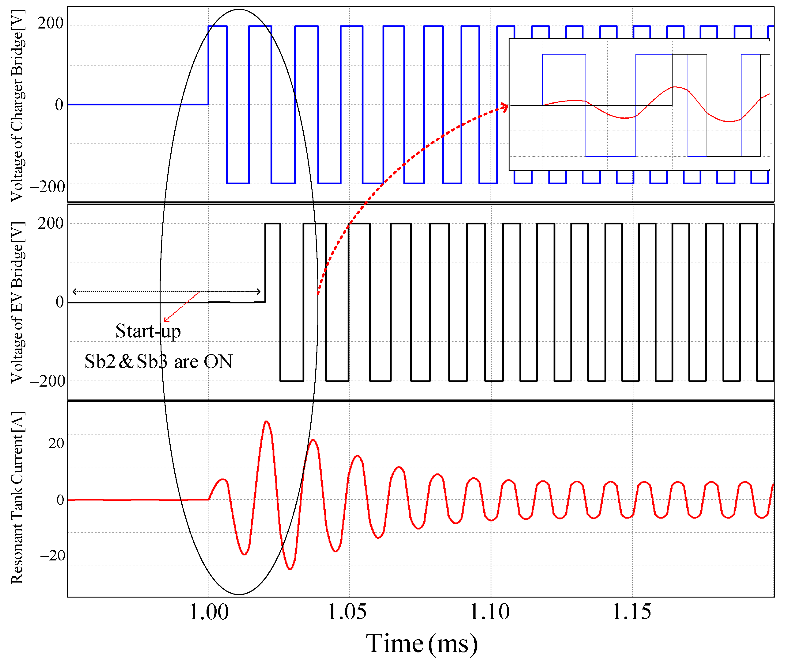
Figure 5 shows the output voltages of the active bridges at start-up, while the tuning loop is set at the lowest output power, the worst case for start-up and achieving ZVS condition.
In this simulation, Sb2 and Sb3 are switched on for about one cycle of the resonant current, about 20 µs, for charging-up of the series resonant tank, as can be seen from
Figure 5. The time constants of the tuning loop are considered as
τ2 = 1 µs and
τ1 = 2 µs and the converter is considered in forward power flow, meaning that the switching states of the charger bridge is determined by zero crossings of the lead phase shifter. As can be seen from
Figure 5, the converter properly starts without current stresses according to its nominal peak current rating for
io, which is about 40 A, moreover, ZVS is achieved at the beginning of the cycles.
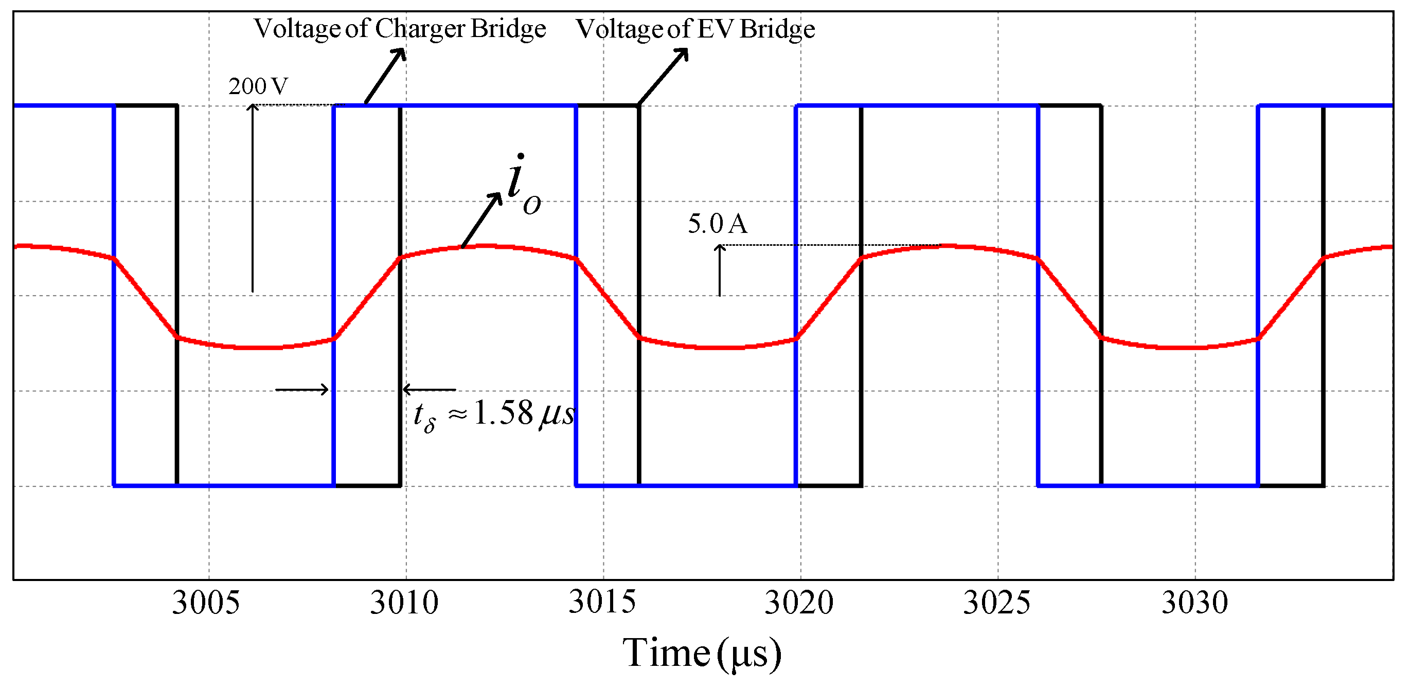
Figure 6 shows the output voltages of the active bridges and the resonant tank current at steady-state condition and forward power direction for
τ2 = 1 µs and
τ1 = 2 µs. It can be seen that ZVS is achieved for the two bridges with minimum phase displacements or circulating currents. In condition of
Figure 6, the transferred power from the right side bridge to the EV side is almost 700 W with operating frequency of about 87.5 kHz. Regarding Equation (16) and
τ2 = 1 µs and
τ1 = 2 µs, the operating frequency is derived about 112.5 kHz. The difference between analysis and simulation result is caused by the non-sinusoidal behavior of
io at light load conditions. To improve this, a new feedback circuit is devised at the end of this section.
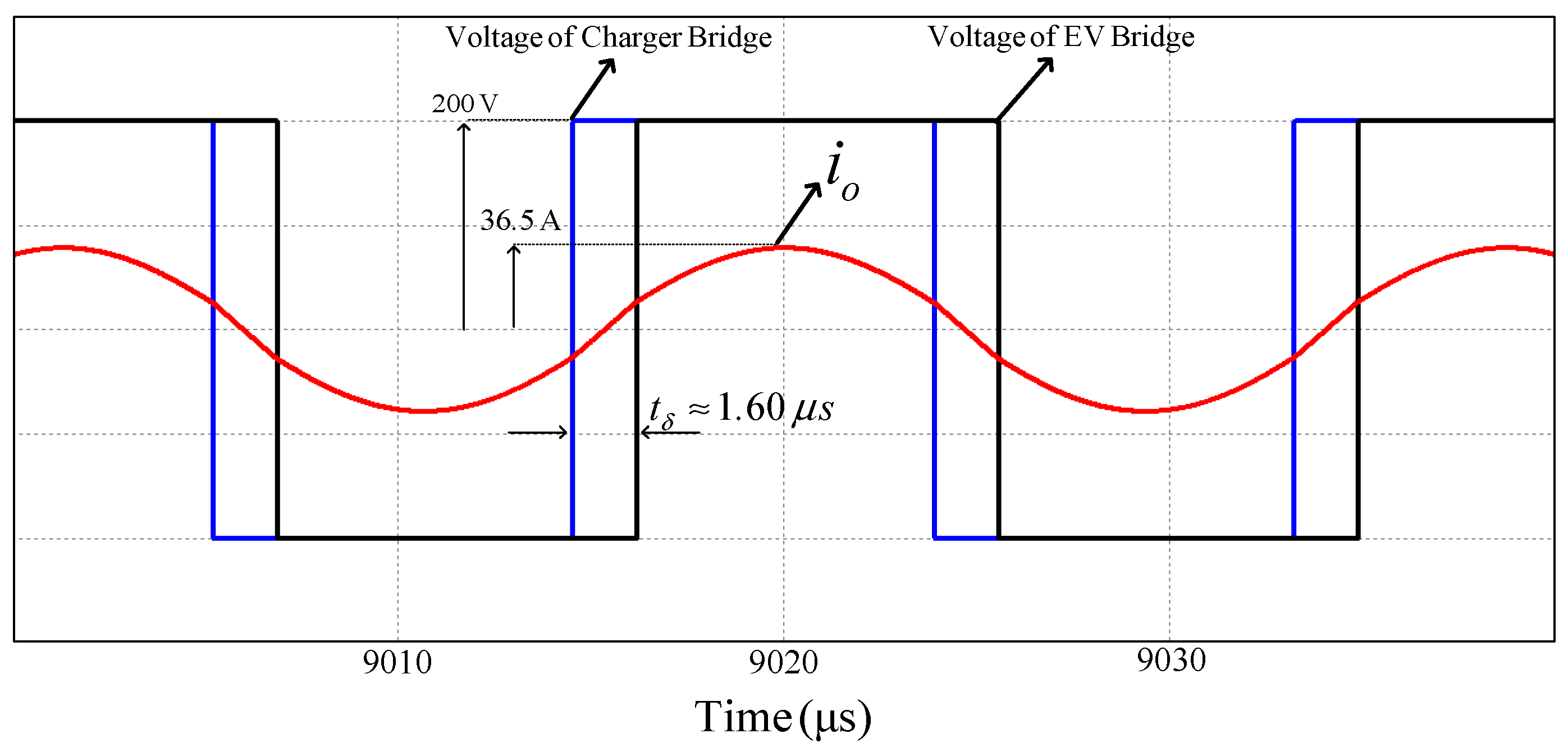
For the maximum power, the converter is simulated for
τ2 = 1 µs and
τ1 = 10 µs and the power direction is considered forward. The output voltages and
io are shown in
Figure 7 which shows that the converter properly operates with the proposed minimum phase displacement at the high power condition. In
Figure 7, the transferred power is about 4.5 kW with operating frequency of 53.4 kHz, which is approximately in fair agreement with Equations (16) and (20).
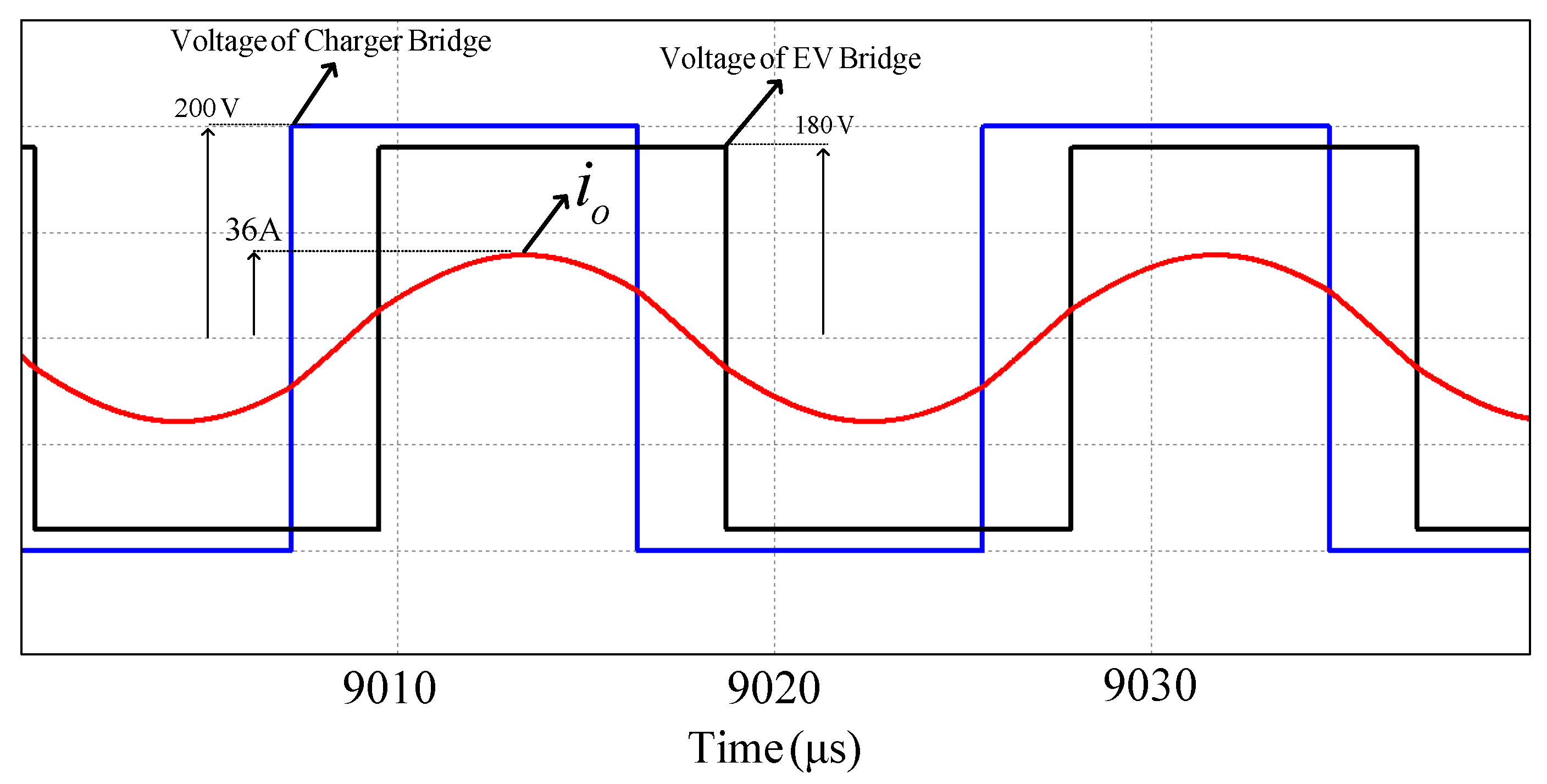
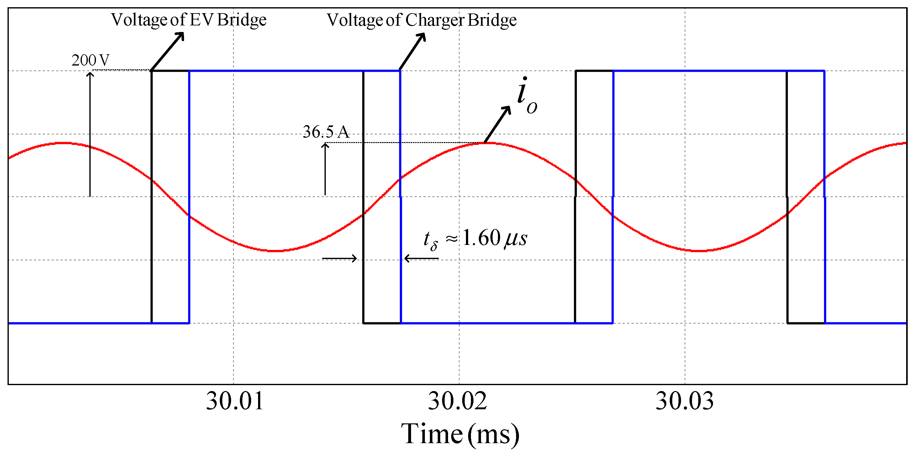
To show the effectiveness of the proposed tuning loop, the unequal DC-link voltages condition is simulated for
Vin = 200 V and
VBatt = 180 V. In the following simulation, the maximum output power is achieved for
τ1 ≈ 4.7 µs while the operating frequency is about 54.5 kHz, as shown in
Figure 8. As can be seen, in this simulation, minimum phase displacement required for ZVS is achieved which shows the proper performance of the proposed tuning loop under unequal DC-link voltages. Regarding simulations, for
VBatt <
Vin, the required time constant to achieve maximum output power occurs between
τ1max and
τ1min derived by (17). Regarding
Figure 6 and
Figure 7,
tδ is approximately constant from low power up to high power conditions. Moreover, regarding simulation results, Equation (19) should be modified to Equation (21).
Moreover, the DC-link of charger sides is connected to an approximately constant DC bus, as shown in
Figure 1. Hence, a well-design HFT can be used to achieve
VBatt ≤
Vin for different conditions and state of charges of batteries. As a result, the tuning loop time constants and DAB-SRC parameters can be designed according to the analysis presented in
Section 3. For large difference in DC-link voltages, the two phase shifters must be considered variable to transfer power in both directions from light load condition up to full load condition.
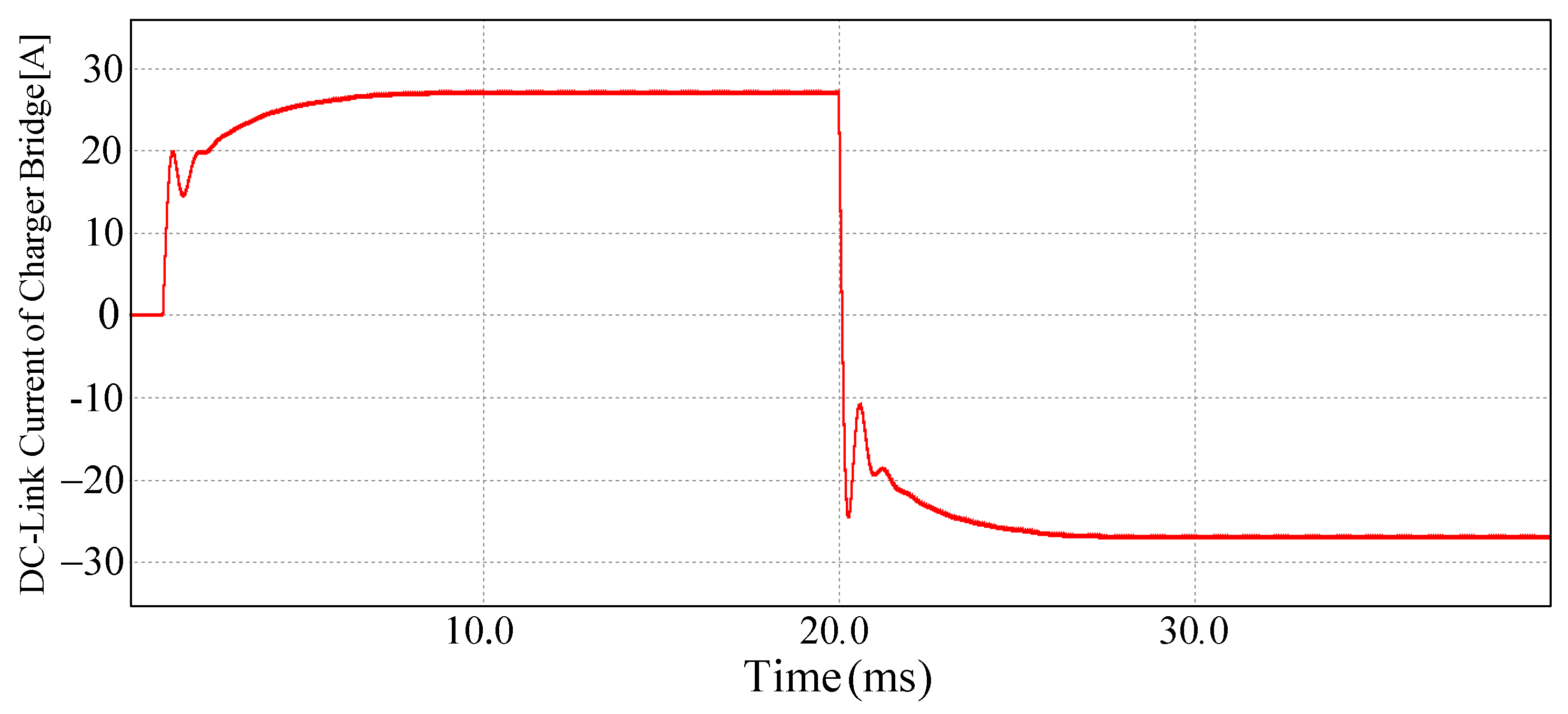
To show the performance of the proposed tuning loop under direction changing of the power flow, a simulation has been undertaken as shown in
Figure 9. In this simulation at
t = 20 ms, the phase shifter of the charger bridge is changed to the fixed lagging phase shifter while the phase shifter of the EV bridge is changed to the variable leading phase shifter.
Figure 9, shows that the tuning loop properly changes the direction of the power flow under full load condition.
Figure 10 shows the output voltages of the two bridges and
io under stead-state condition and backward direction of power flow with transferred power of about 4.5 kW and operating frequency of about 54.5 kHz. The following simulations show that ZVS and minimum phase displacement can be achieved similar to the forward direction with a fast transient.
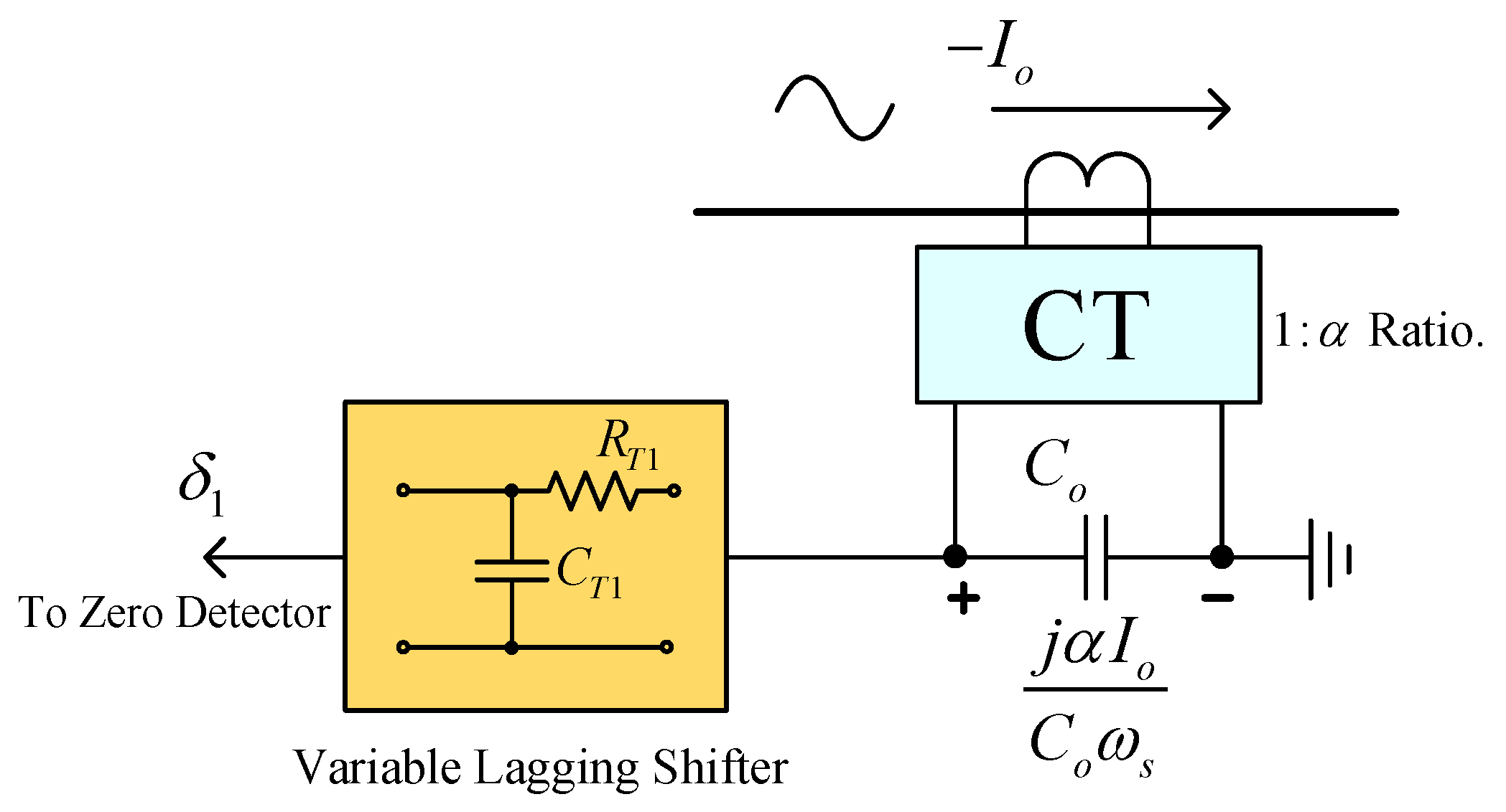
To improve the accuracy of the proposed tuning loop, a new feedback circuit for the power generator bridge is devised, as shown in
Figure 11. In this circuit, output of the CT is directly connected to a capacitive load,
Co, in comparison with conventional CT circuits which utilizes a resistive load. Hence, regarding
Figure 11 and effect of
Co, the output signal of the CT is 90
0 lead with respect to
io. Using a variable lagging phase shifter with the same
RT1 and
CT1,
δ1 can be derived by (22) which is similar to Equation (12). Therefore, without any change in the previous analysis,
Co and the variable low pass filter, effectively suppress the high order harmonics.
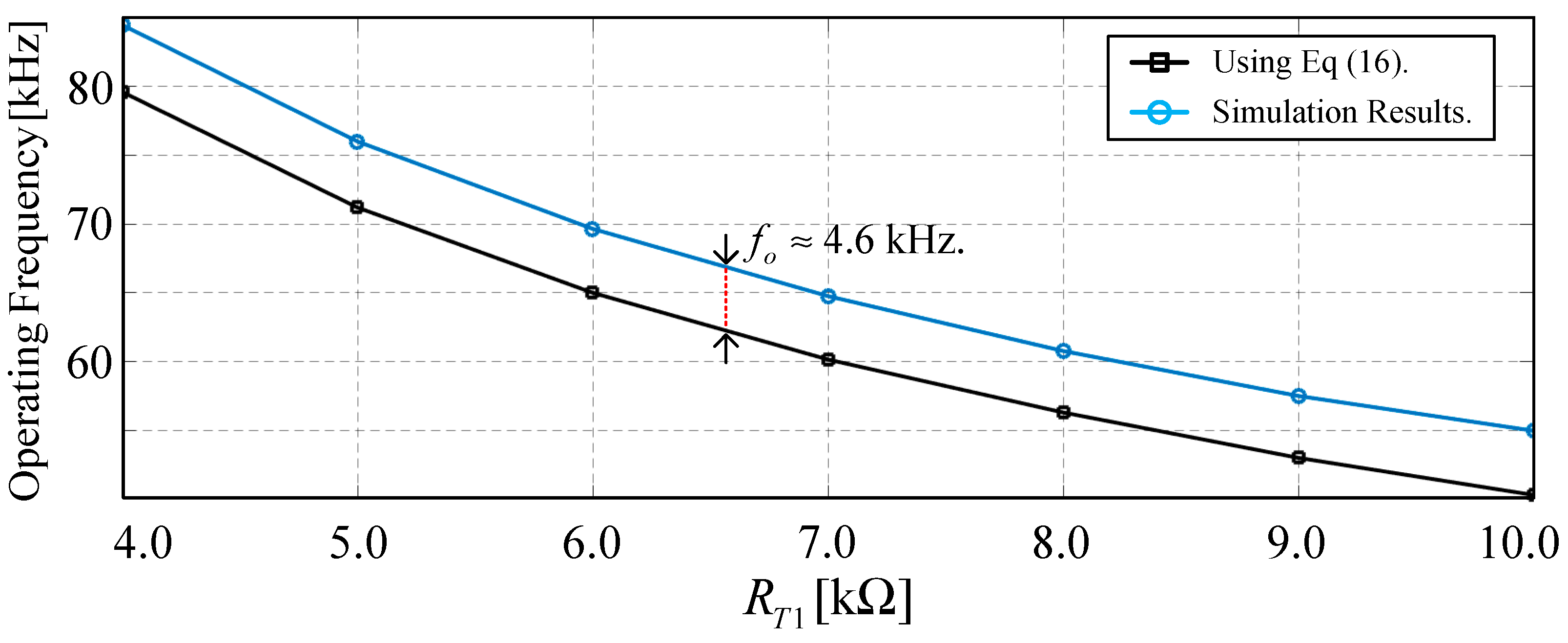
Figure 12 shows dependency of the converter’s operating frequency against
RT1 using (16) beside the simulation results, based on the new feedback circuit for the charger bridge, i.e., the forward power direction. In this figure, the operating frequency is derived for different tuning resistors,
RT1, for the variable lagging phase shifter and in a wide range of operating frequencies, i.e. 51 kHz up to 85 kHz. Regarding
Figure 12, there is only a fixed offset,
fo ≈ 4.6 kHz, between the analysis and the simulation results. Hence, Equation (16) should be revised to the following equation:
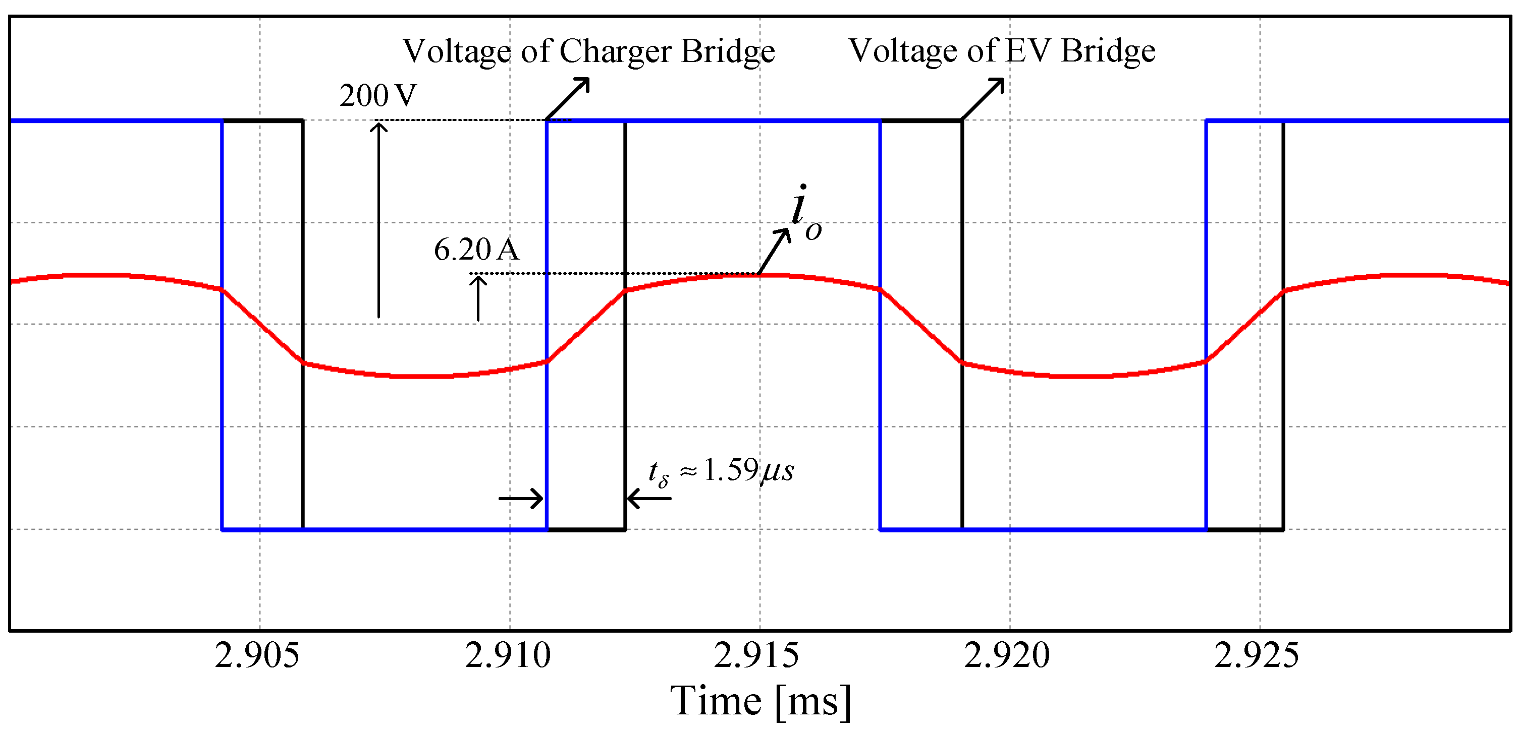
To validate the above modification, a simulation is undertaken using previous parameters for the DAB-SRC, as shown in
Figure 13. In the following simulation, the new feedback circuit is used for the charger bridge with
CT1 = 1 nF and
RT1 = 5 kΩ. At the steady state, the operating frequency of the system is about 75.78 kHz, while using (22) the operating frequency is derived at about 75.77 kHz, which shows the accuracy of the tuning loop based on the new feedback circuit. Moreover, regarding
Figure 13, the time displacement between,
tδ, active bridges is about 1.59 µs which is compatible with Equation (21).
For the fixed offset,
fo, a sensitivity analysis based on more than 200 simulations with different resonant tank parameters and different
τ1 and
τ2 has been undertaken. Based on the analysis,
fo is only related to the fixed time constant, i.e.,
τ2. The relationship between
fo and
τ2 is derived by the following which has maximum error 3% for all scenarios in the sensitivity analysis.
5. Experimental Results
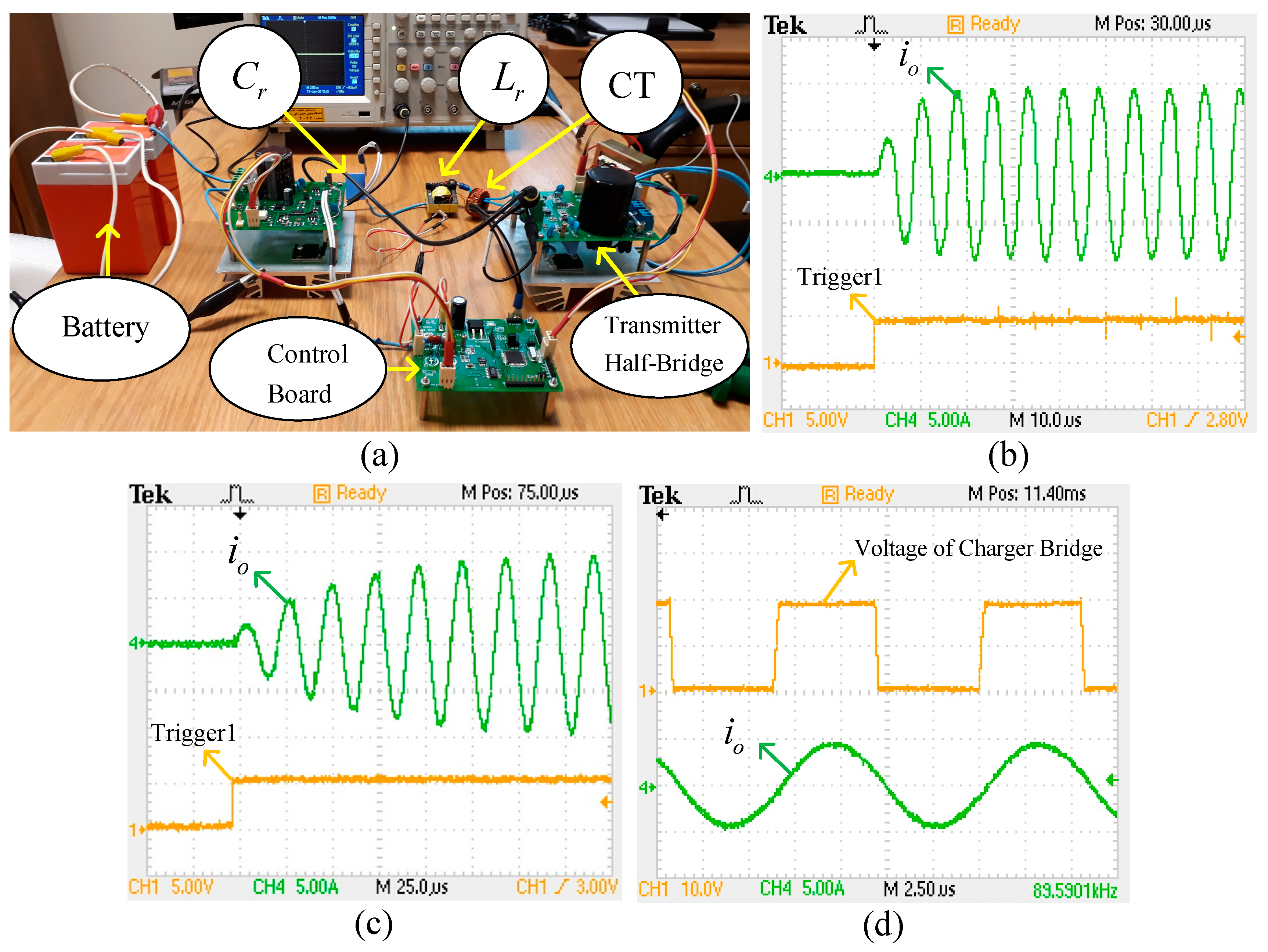
For simplicity, experimental results of the SRC are derived based on dual-active half-brides, connected together by resonant capacitor and inductor, as shown in
Figure 14a. In this setup, the resonant inductor is about 15 µH and different resonant capacitors are used to assess the validity of the proposed tuning loop under different resonant frequencies. The power switches are IRFP260N power MOSFETs while the drivers are implemented by IR2104S bootstrap gate drivers.
The MCU is ATMEGA16 with 8 MHz clock pulse and the zero detector circuits are constructed using LT1016 comparators with sensitivity of 5 mV and propagation delay of about 10 ns. It is worth noting that using 32-bit micro-controllers is essential for final fabrication and better dynamic responses. The CT turn ratio is 100 and a 100 Ω resistor is connected to the CT, i.e. 1ampere/volt gain. In this setup, one of the half bridge DC-link is directly connected to a battery bank with voltage of about 20 V. Moreover, for the power transmitter half-bridge, the DC-link voltage is set to 20 V.
Figure 14b shows
io and Trigger1 signal at start-up condition while
τ1 ≈ 2.2 µs and
τ2 ≈ 1 µs. Regarding this figure, the operating frequency is about 109.6 kHz which is derived from about 111.9 kHz using Equations (23) and (24). In this result the resonant capacitor is about 180 nF.
Figure 14c shows the start-up condition for the same signals while
τ1 ≈ 16 µs,
τ2 ≈ 1 µs and the resonant capacitor is about 1200 nF. Regarding this figure, the operating frequency is about 44.4 kHz which is also compatible with Equations (23) and (24) with less than 3% error.
Figure 14d, shows the output current and voltage of the charger inverter at steady state, while ZVS is achieved with a minimum phase displacement with
τ1 ≈ 3.6 µs,
τ2 ≈ 1 µs and the resonant capacitor is about 400 nF. Operating frequency is about 89.6 kHz while using Equations (23) and (24), the operating frequency is about 88.5 kHz. Experimental results show the accuracy of the previous analysis and the new tuning loop can be considered as a simple and fast tuning loop for DAB-SRC.


