A Compact and Robust Technique for the Modeling and Parameter Extraction of Carbon Nanotube Field Effect Transistors

 ,
,  ,
,  ,
,  ,
,  ,
,  , and
, and
Abstract
:1. Introduction
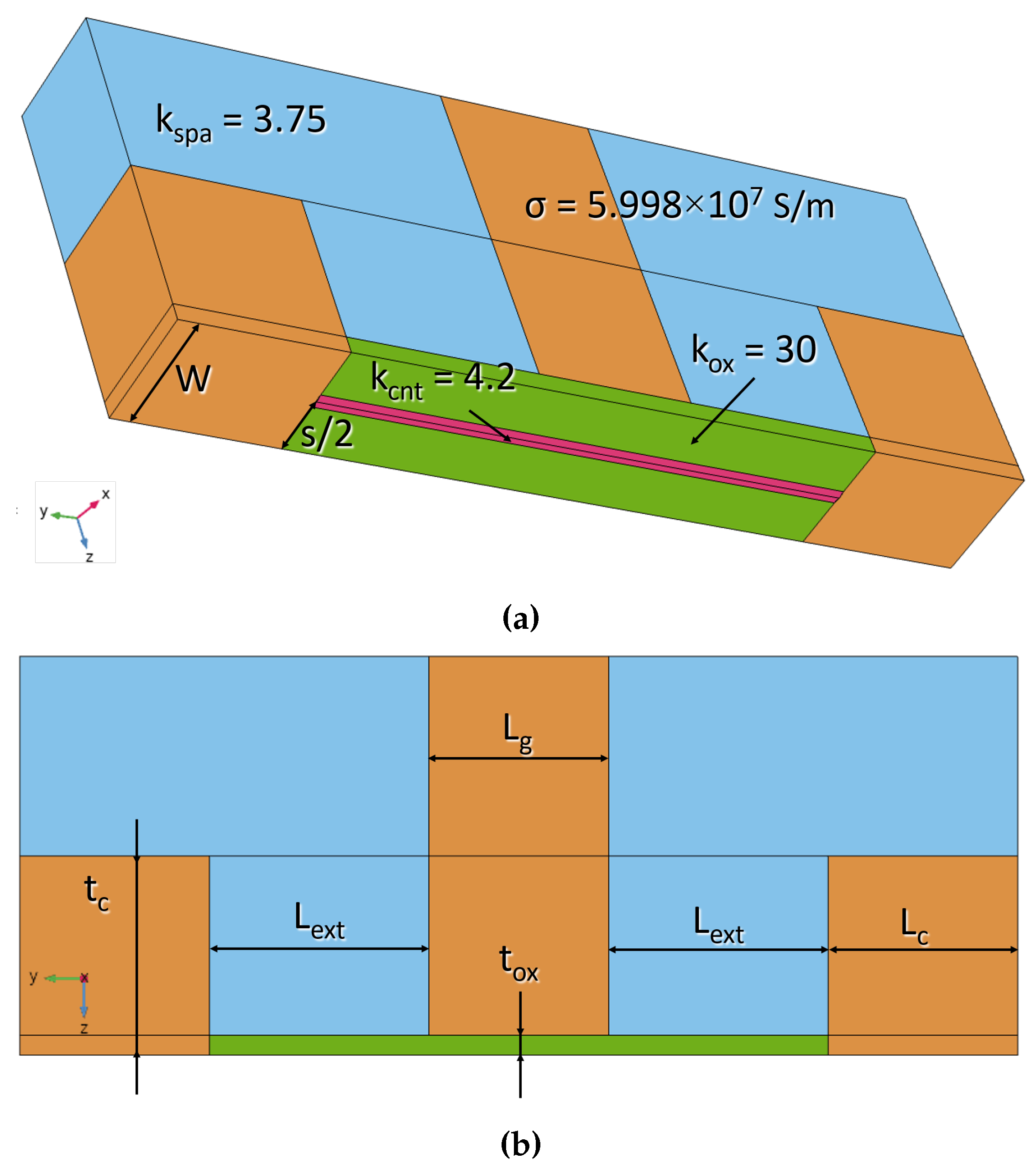
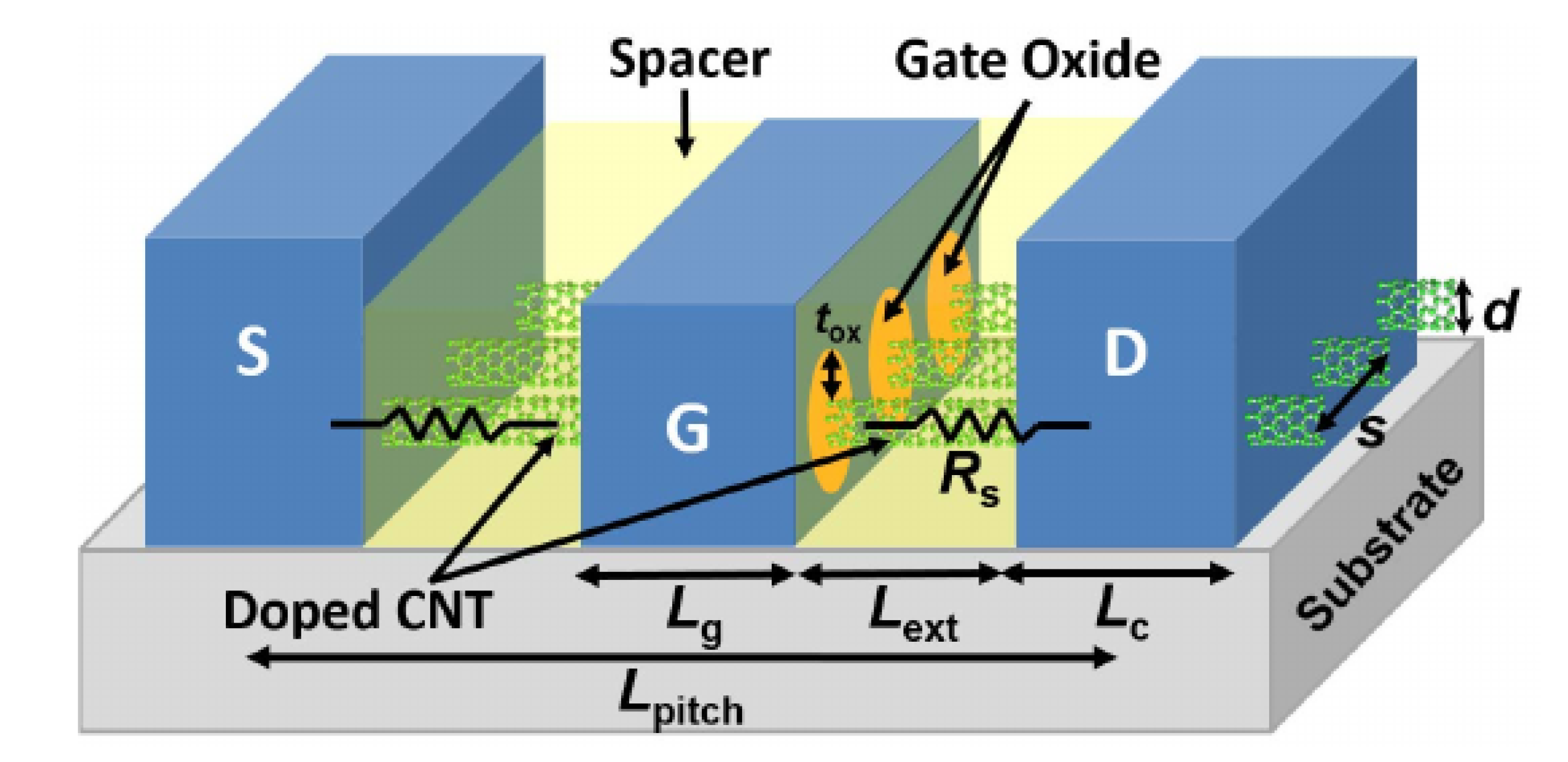
2. Full-Wave Simulation
- The Matlab procedure calculates the charge inside the tube, considering a null electric potential, and then provides it to COMSOL as an input;
- COMSOL calculates the electric potential in each point of the device, including the nanotube;
- The electric potential along the tube is provided to the Matlab procedure, then the loop is repeated until convergence is reached.
3. Formulation of the Compact CNTFET Model
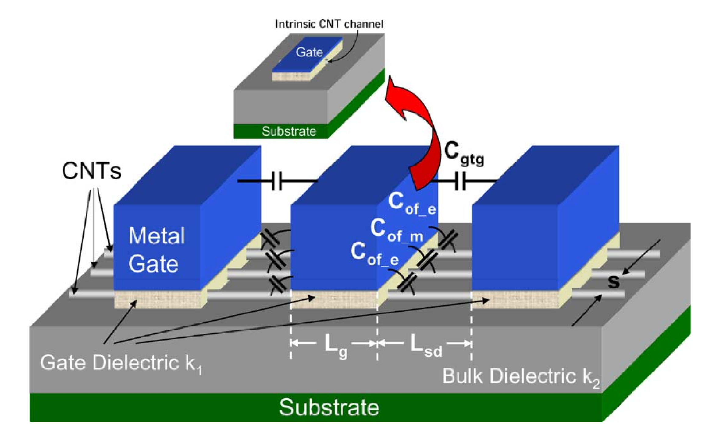
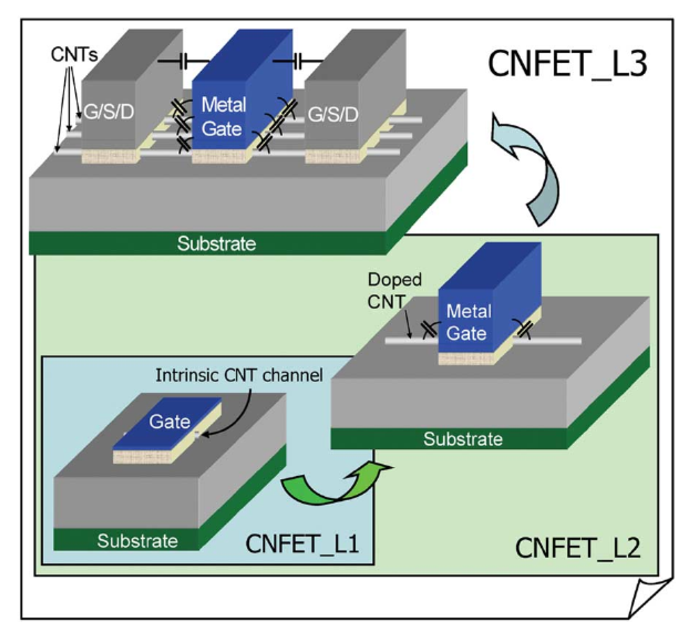
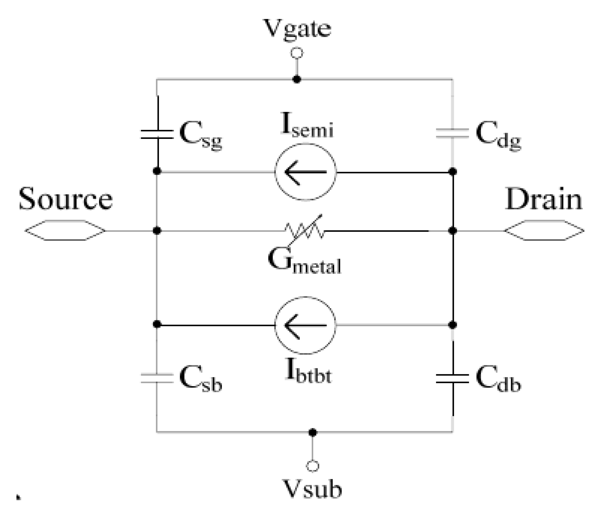
3.1. A Circuit Compatible SPICE Model for CNTFET
CNTFET Device Model Level 1
3.2. A Compact Virtual-Source Model for CNT
VS Model for CNTFET
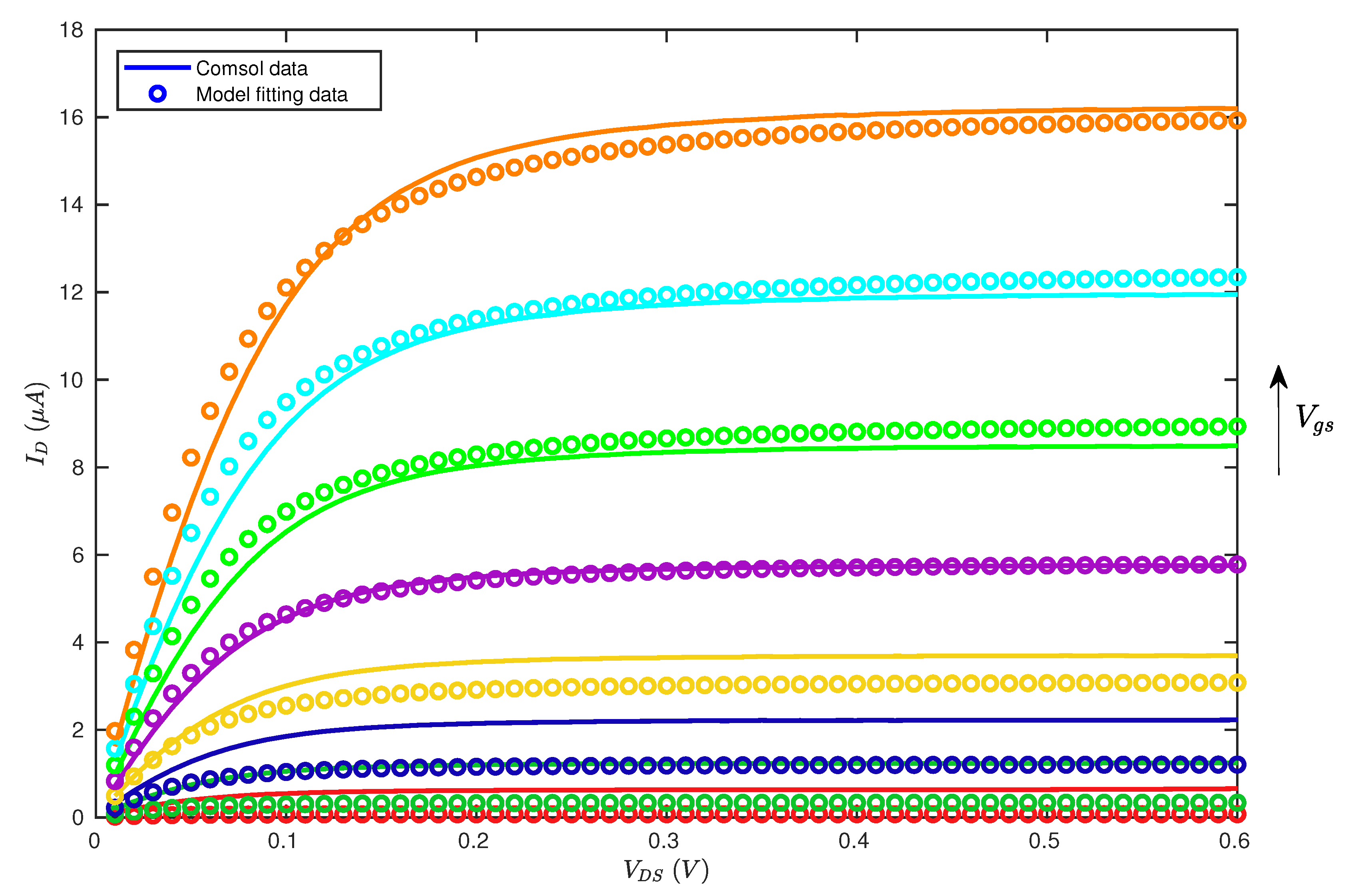
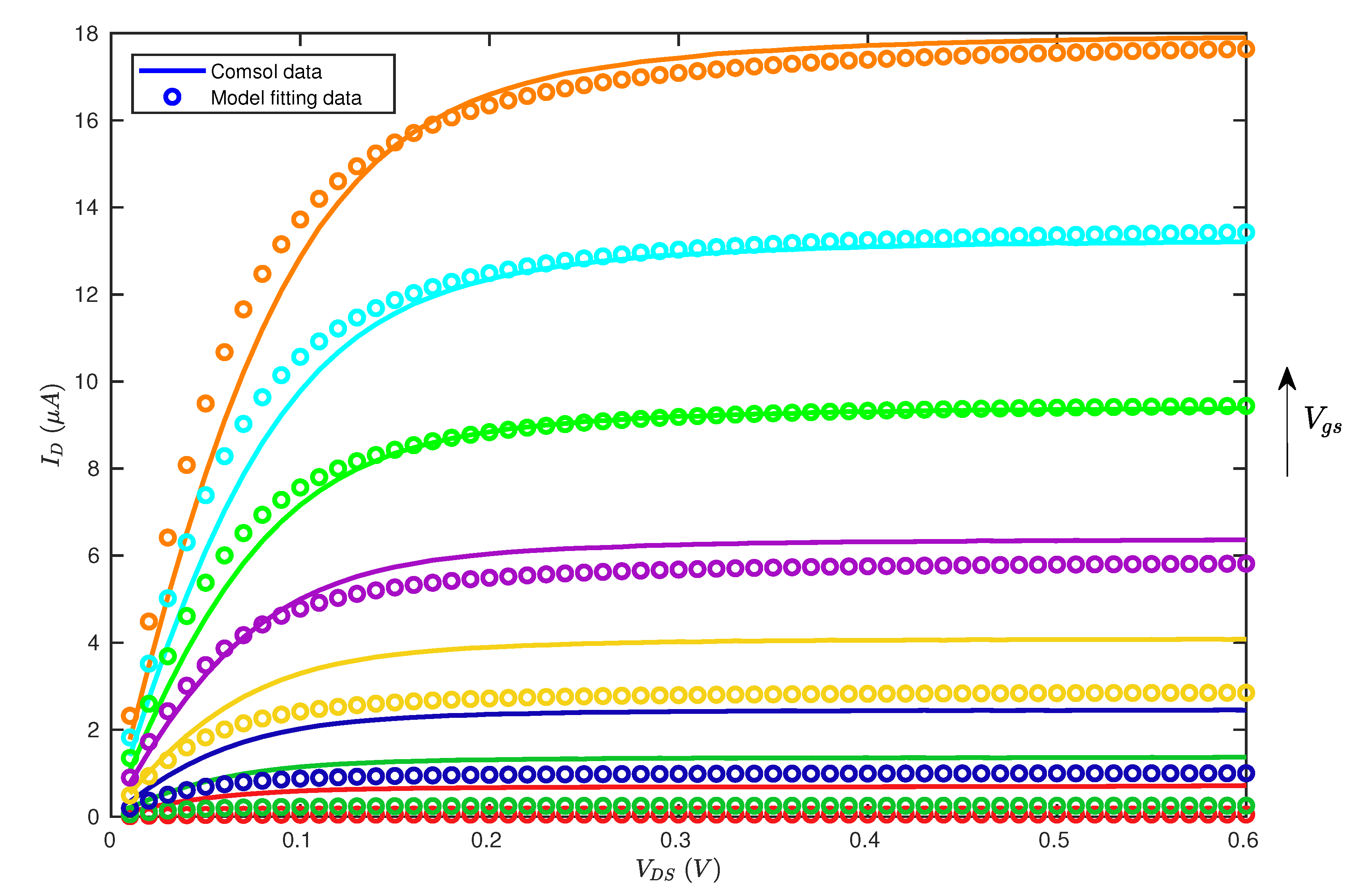
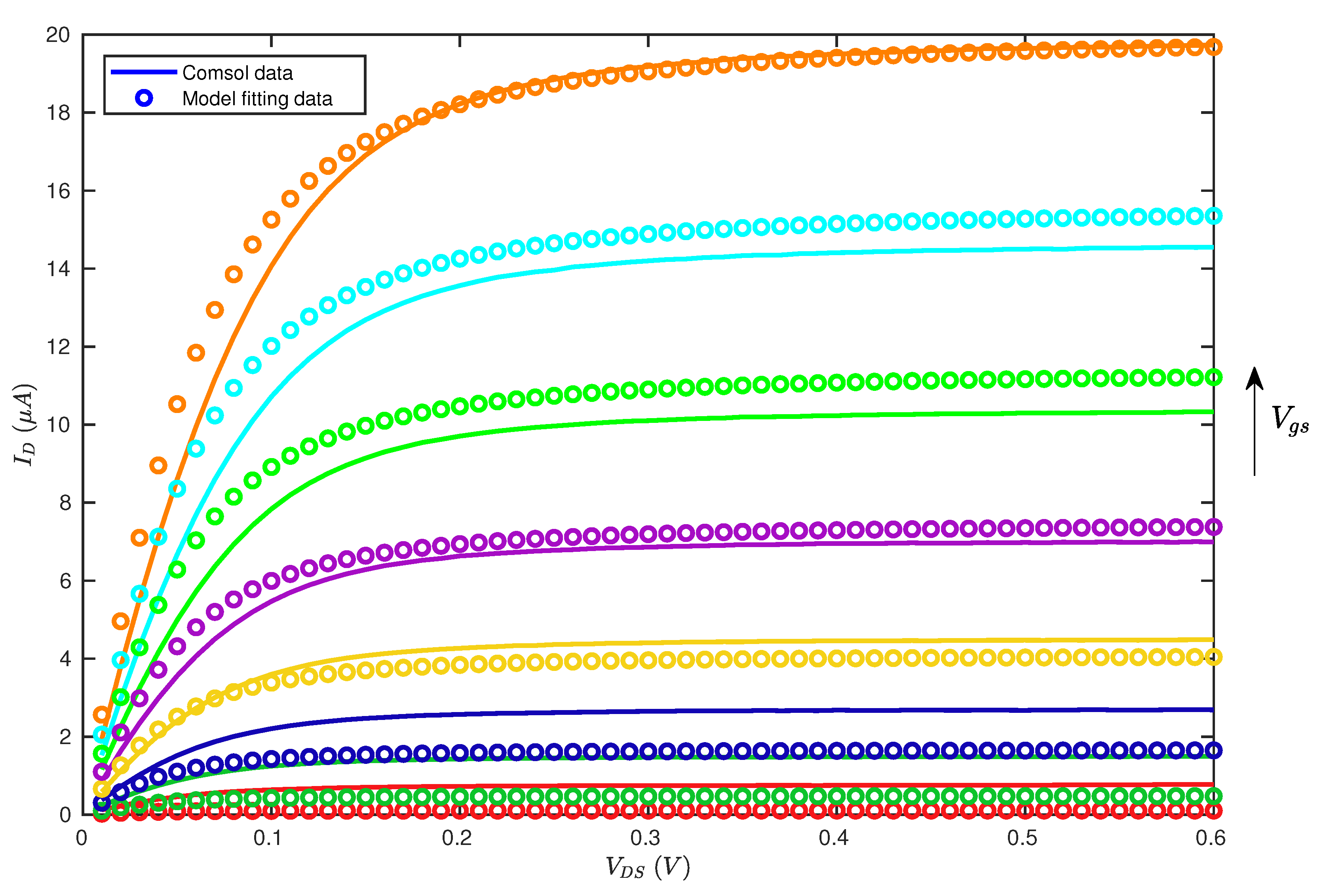
4. Results and Discussion
4.1. Model Fitting
4.2. Simulations Results
5. Conclusions
Author Contributions
Funding
Conflicts of Interest
References
- Mencarelli, D.; Rozzi, T.; Camilloni, C.; Maccari, L.; di Donato, A.; Pierantoni, L. Modelling of multi-wall CNT devices by self-consistent analysis of multichannel transport. Nanotechnology 2008, 19, 165202. [Google Scholar] [CrossRef] [PubMed]
- Bishop, M.; Hills, G.; Srimani, T.; Lau, C.; Murphy, D.; Fuller, S.; Humes, J.; Ratkovich, A.; Nelson, M.; Shulaker, M. Fabrication of carbon nanotube field-effect transistors in commercial silicon manufacturing facilities. Nat. Electron. 2020, 3, 492–501. [Google Scholar] [CrossRef]
- Mao, S. Chapter 5-Graphene Field-Effect Transistor Sensors. In Graphene Bioelectronics; Tiwari, A., Ed.; Advanced Nanomaterials; Elsevier: Amsterdam, The Netherlands, 2018; pp. 113–132. [Google Scholar]
- Mencarelli, D.; Rozzi, T.; Pierantoni, L. Coherent carrier transport and scattering by lattice defects in single- and multibranch carbon nanoribbons. Phys. Rev. B Condens. Matter Mater. Phys. 2008, 77. [Google Scholar] [CrossRef]
- Deng, J.; Wong, H.P. A Compact SPICE Model for Carbon-Nanotube Field-Effect Transistors Including non-idealities and Its Application—Part I: Model of the Intrinsic Channel Region. IEEE Trans. Electron Devices 2007, 54, 3186–3194. [Google Scholar] [CrossRef]
- Deng, J.; Wong, H.P. A Compact SPICE Model for Carbon-Nanotube Field-Effect Transistors Including non-idealities and Its Application—Part II: Full Device Model and Circuit Performance Benchmarking. IEEE Trans. Electron Devices 2007, 54, 3195–3205. [Google Scholar] [CrossRef]
- Luo, J.; Wei, L.; Lee, C.; Franklin, A.D.; Guan, X.; Pop, E.; Antoniadis, D.A.; Wong, H.P. Compact Model for Carbon Nanotube Field-Effect Transistors Including non-idealities and Calibrated With Experimental Data Down to 9-nm Gate Length. IEEE Trans. Electron Devices 2013, 60, 1834–1843. [Google Scholar] [CrossRef]
- Khakifirooz, A.; Nayfeh, O.M.; Antoniadis, D. A Simple Semiempirical Short-Channel MOSFET Current-Voltage Model Continuous Across All Regions of Operation and Employing Only Physical Parameters. IEEE Trans. Electron Devices 2009, 56, 1674–1680. [Google Scholar] [CrossRef]
- Lee, C.S.; Pop, E.; Franklin, A.D.; Haensch, W.; Wong, H.S.P. A Compact Virtual-Source Model for Carbon Nanotube FETs in the Sub-10-nm Regime—Part I: Intrinsic Elements. IEEE Trans. Electron Devices 2015, 62, 3061–3069. [Google Scholar] [CrossRef] [Green Version]
- Lee, C.S.; Pop, E.; Franklin, A.D.; Haensch, W.; Wong, H.S.P. A Compact Virtual-Source Model for Carbon Nanotube FETs in the Sub-10-nm Regime—Part II: Extrinsic Elements, Performance Assessment, and Design Optimization. IEEE Trans. Electron Devices 2015, 62, 3070–3078. [Google Scholar] [CrossRef] [Green Version]
- Vincenzi, G.; Deligeorgis, G.; Coccetti, F.; Dragoman, M.; Pierantoni, L.; Mencarelli, D.; Plana, R. Extending ballistic graphene FET lumped element models to diffusive devices. Solid-State Electron. 2012, 76, 8–12. [Google Scholar] [CrossRef] [Green Version]
- Bethoux, J.; Happy, H.; Dambrine, G.; Derycke, V.; Goffman, M.; Bourgoin, J. An 8-GHz f/sub t/ carbon nanotube field-effect transistor for gigahertz range applications. IEEE Electron Device Lett. 2006, 27, 681–683. [Google Scholar] [CrossRef]
- Zhang, H.; Pesetski, A.A.; Baumgardner, J.E.; Murduck, J.M.; Przybysz, J.X.; Adam, J.D. K-band Carbon Nanotube FET Operation. In Proceedings of the 2006 IEEE MTT-S International Microwave Symposium Digest, San Francisco, CA, USA, 11–16 June 2006; pp. 1688–1691. [Google Scholar]
- Shulaker, M.M.; Pitner, G.; Hills, G.; Giachino, M.; Wong, H.P.; Mitra, S. High-performance carbon nanotube field-effect transistors. In Proceedings of the 2014 IEEE International Electron Devices Meeting, San Francisco, CA, USA, 15–17 December 2014; pp. 33.6.1–33.6.4. [Google Scholar]
- Raychowdhury, A.; Mukhopadhyay, S.; Roy, K. A circuit-compatible model of ballistic carbon nanotube field-effect transistors. IEEE Trans. Comput. Aided Des. Integr. Circuits Syst. 2004, 23, 1411–1420. [Google Scholar] [CrossRef]
- Fregonese, S.; Cazin d’Honincthun, H.; Goguet, J.; Maneux, C.; Zimmer, T.; Bourgoin, J.; Dollfus, P.; Galdin-Retailleau, S. Computationally Efficient Physics-Based Compact CNTFET Model for Circuit Design. IEEE Trans. Electron Devices 2008, 55, 1317–1327. [Google Scholar] [CrossRef]
- Goguet, J.; Fregonese, S.; Maneux, C.; Zimmer, T. Compact Model of a Dual Gate CNTFET: Description and Circuit Application. In Proceedings of the 2008 8th IEEE Conference on Nanotechnology, Arlington, TX, USA, 18–21 August 2008; pp. 388–389. [Google Scholar]
- Wei, L.; Frank, D.J.; Chang, L.; Wong, H.P. A non-iterative compact model for carbon nanotube FETs incorporating source exhaustion effects. In Proceedings of the 2009 IEEE International Electron Devices Meeting (IEDM), Baltimore, MD, USA, 7–9 December 2009; pp. 1–4. [Google Scholar]
- Balijepalli, A.; Sinha, S.; Cao, Y. Compact modeling of carbon nanotube transistor for early stage process-design exploration. In Proceedings of the 2007 International Symposium on Low Power Electronics and Design (ISLPED ’07), Portland, OR, USA, 27–29 August 2007; pp. 2–7. [Google Scholar]
- Sinha, S.; Balijepalli, A.; Cao, Y. Compact Model of Carbon Nanotube Transistor and Interconnect. IEEE Trans. Electron Devices 2009, 56, 2232–2242. [Google Scholar] [CrossRef]
- Pregaldiny, F.; Lallement, C.; Kammerer, J. Design-oriented compact models for CNTFETs. In Proceedings of the International Conference on Design and Test of Integrated Systems in Nanoscale Technology, 2006. DTIS 2006, Tunis, Tunisia, 5–7 September 2006; pp. 34–39. [Google Scholar]
- Yamacli, S.; Avci, M. Accurate SPICE compatible CNT interconnect and CNTFET models for circuit design and simulation. Math. Comput. Model. 2013, 58, 368–378. [Google Scholar] [CrossRef]
- Rakheja, S.; Antoniadis, D. MVS Nanotransistor Model (Silicon). 2015. Available online: https://nanohub.org/publications/15/4 (accessed on 8 October 2020).
- Verilog-A Language Reference Manual: Analog Extensions to Verilog HDL; Open Verilog International: Los Gatos, CA, USA, 1996.
- Lee, C.S.; Wong, H.S.P. Stanford Virtual-Source Carbon Nanotube Field-Effect Transistors Model. 2015. Available online: https://nanohub.org/publications/42/2 (accessed on 8 October 2020).
- Kirkpatrick, S.; Gelatt, C.D.; Vecchi, M.P. Optimization by simulated annealing. Science 1983, 220, 671–680. [Google Scholar] [CrossRef] [PubMed]
- Van Laarhoven, P.J.; Aarts, E.H. Simulated annealing. In Simulated Annealing: Theory and Applications; Springer: Dordrecht, The Netherlands, 1987; pp. 7–15. [Google Scholar]


| Name | Description | Type |
|---|---|---|
| s | spacing between the CNTs (center-to-center) (m) | geometrical |
| W | transistor width (m) | geometrical |
| physical gate length (m) | geometrical | |
| gate height (m) | geometrical | |
| contact length (m) | geometrical | |
| source/drain extension length or spacer length (m) | geometrical | |
| d | CNT diameter (m) | geometrical |
| gate oxide thickness (m) | physical | |
| gate oxide dielectric constant | physical | |
| CNT dielectric constant | physical | |
| substrate dielectric constant | physical | |
| source/drain spacer dielectric constant | physical | |
| Fermi level to the band edge (eV) at the source/drain, related to the doping density | physical | |
| flat band voltage (V) (for threshold voltage adjustment) | physical | |
| device geometry | geometrical | |
| contact mode | physical | |
| user-defined series resistance () | physical | |
| source-to-drain tunneling (SDT) mode | physical | |
| band-to-band tunneling mode | physical | |
| T | temperature (°C) | physical |
| Name | Value |
|---|---|
| s | 10 nm |
| W | 1 m |
| 90 nm, 190 nm, 290 nm | |
| 5 nm | |
| d | 1.26 nm |
| 10 nm | |
| 30 | |
| 4.2 | |
| 3.75 | |
| 0.5557 eV | |
| top-gate | |
| off | |
| on | |
| T | 16.85 °C (290 K) |
| Name | Description |
|---|---|
| gate capacitance in strong inversion region (F/m) | |
| low-field effective mobility (mVs) | |
| threshold voltage (V) | |
| n (SS) | inverse subthreshold slope factor (V/dec) |
| (DIBL) | drain-induced barrier lowering coefficient (V/V) |
| series resistance () | |
| VS carrier velocity (m/s) | |
| CNT quantum capacitance param 1 (F/m) | |
| CNT quantum capacitance param 2 (F/m) |
| Parameter | nm | nm | nm |
|---|---|---|---|
| (fF/m) | 0.761 | 1.571 | 2.206 |
| (cmVs) | 1100 | 1416 | 1554 |
| (V) | 0.549 | 0.564 | 0.543 |
| SS (mV/dec) | 100 | 100 | 100 |
| DIBL (V/V) | 0.760 | 0.787 | 0.751 |
| (k) | 0.554 | 8.135 | 0.479 |
| (cm/s) | 1.030 | 5.937 | 0.427 |
| (fF/m) | 0.022 | 0.027 | 0.012 |
| (fF/m) | 0.011 | 0.006 | 0.034 |
Publisher’s Note: MDPI stays neutral with regard to jurisdictional claims in published maps and institutional affiliations. |
© 2020 by the authors. Licensee MDPI, Basel, Switzerland. This article is an open access article distributed under the terms and conditions of the Creative Commons Attribution (CC BY) license (http://creativecommons.org/licenses/by/4.0/).
Share and Cite
Falaschetti, L.; Mencarelli, D.; Pelagalli, N.; Crippa, P.; Biagetti, G.; Turchetti, C.; Deligeorgis, G.; Pierantoni, L. A Compact and Robust Technique for the Modeling and Parameter Extraction of Carbon Nanotube Field Effect Transistors. Electronics 2020, 9, 2199. https://doi.org/10.3390/electronics9122199
Falaschetti L, Mencarelli D, Pelagalli N, Crippa P, Biagetti G, Turchetti C, Deligeorgis G, Pierantoni L. A Compact and Robust Technique for the Modeling and Parameter Extraction of Carbon Nanotube Field Effect Transistors. Electronics. 2020; 9(12):2199. https://doi.org/10.3390/electronics9122199
Chicago/Turabian StyleFalaschetti, Laura, Davide Mencarelli, Nicola Pelagalli, Paolo Crippa, Giorgio Biagetti, Claudio Turchetti, George Deligeorgis, and Luca Pierantoni. 2020. "A Compact and Robust Technique for the Modeling and Parameter Extraction of Carbon Nanotube Field Effect Transistors" Electronics 9, no. 12: 2199. https://doi.org/10.3390/electronics9122199
APA StyleFalaschetti, L., Mencarelli, D., Pelagalli, N., Crippa, P., Biagetti, G., Turchetti, C., Deligeorgis, G., & Pierantoni, L. (2020). A Compact and Robust Technique for the Modeling and Parameter Extraction of Carbon Nanotube Field Effect Transistors. Electronics, 9(12), 2199. https://doi.org/10.3390/electronics9122199