Contact Resistance Parallel Model for Edge-Contacted 2D Material Back-Gate FET


Abstract
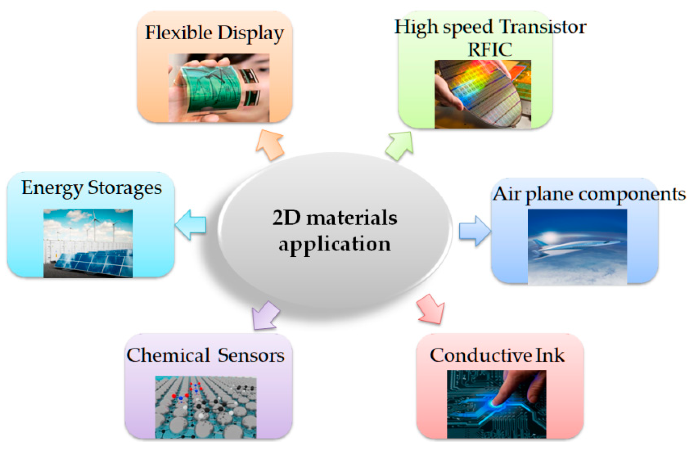
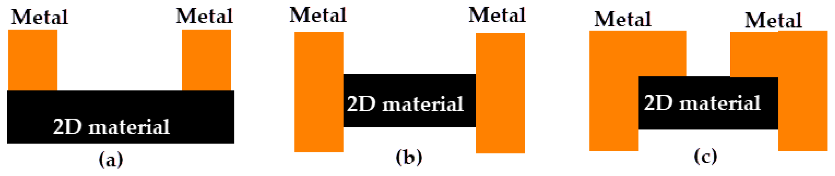
1. Introduction
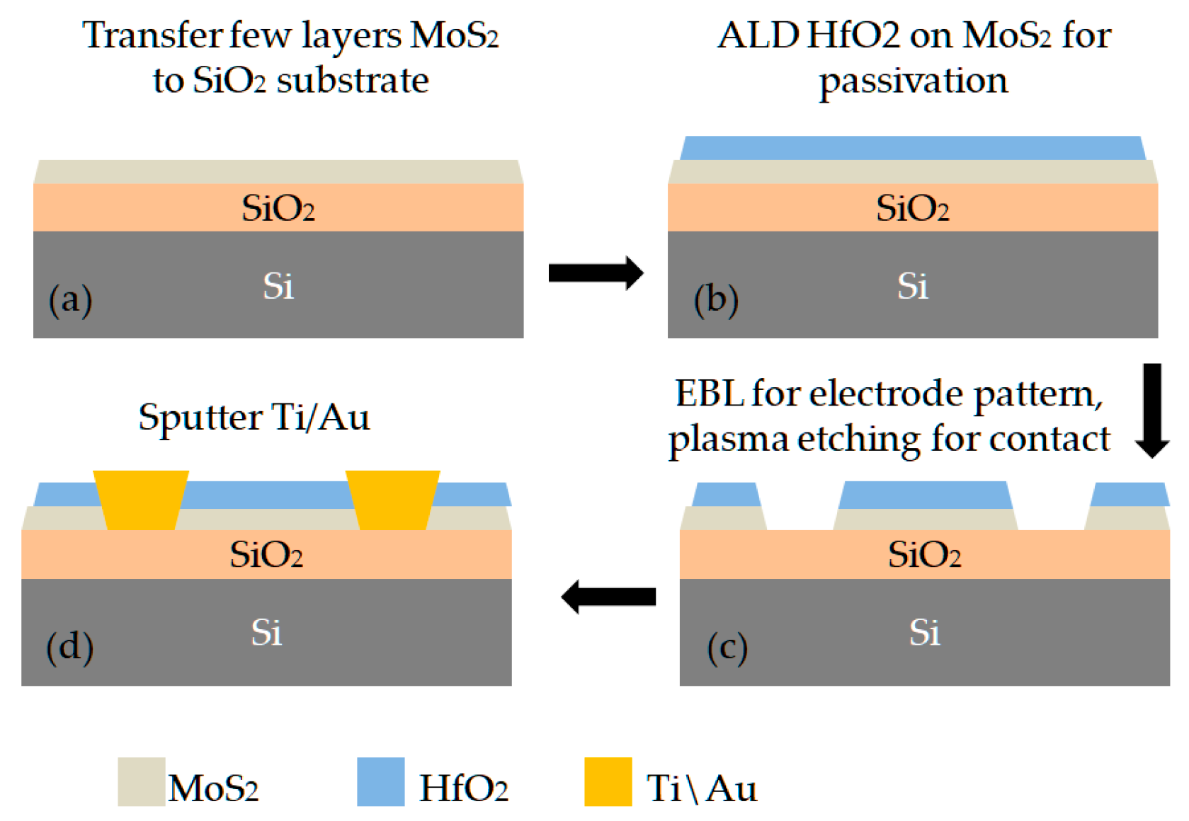
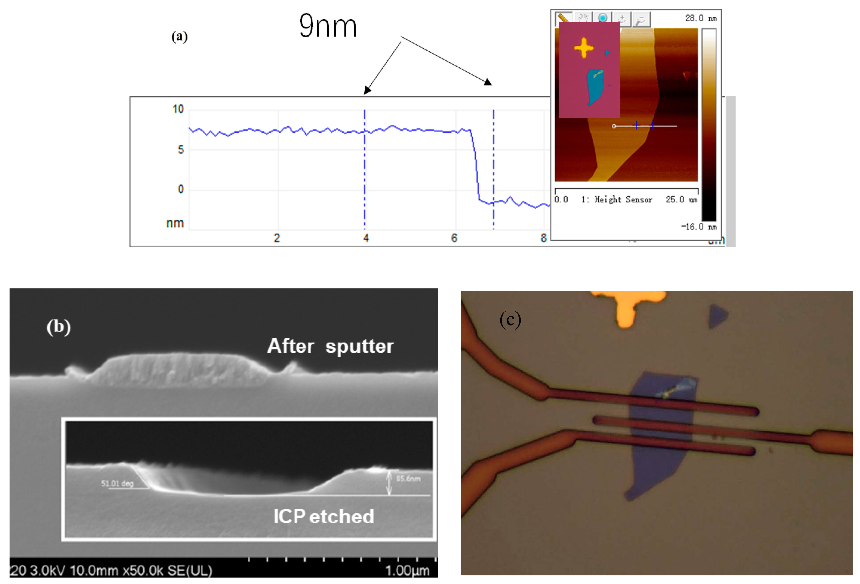
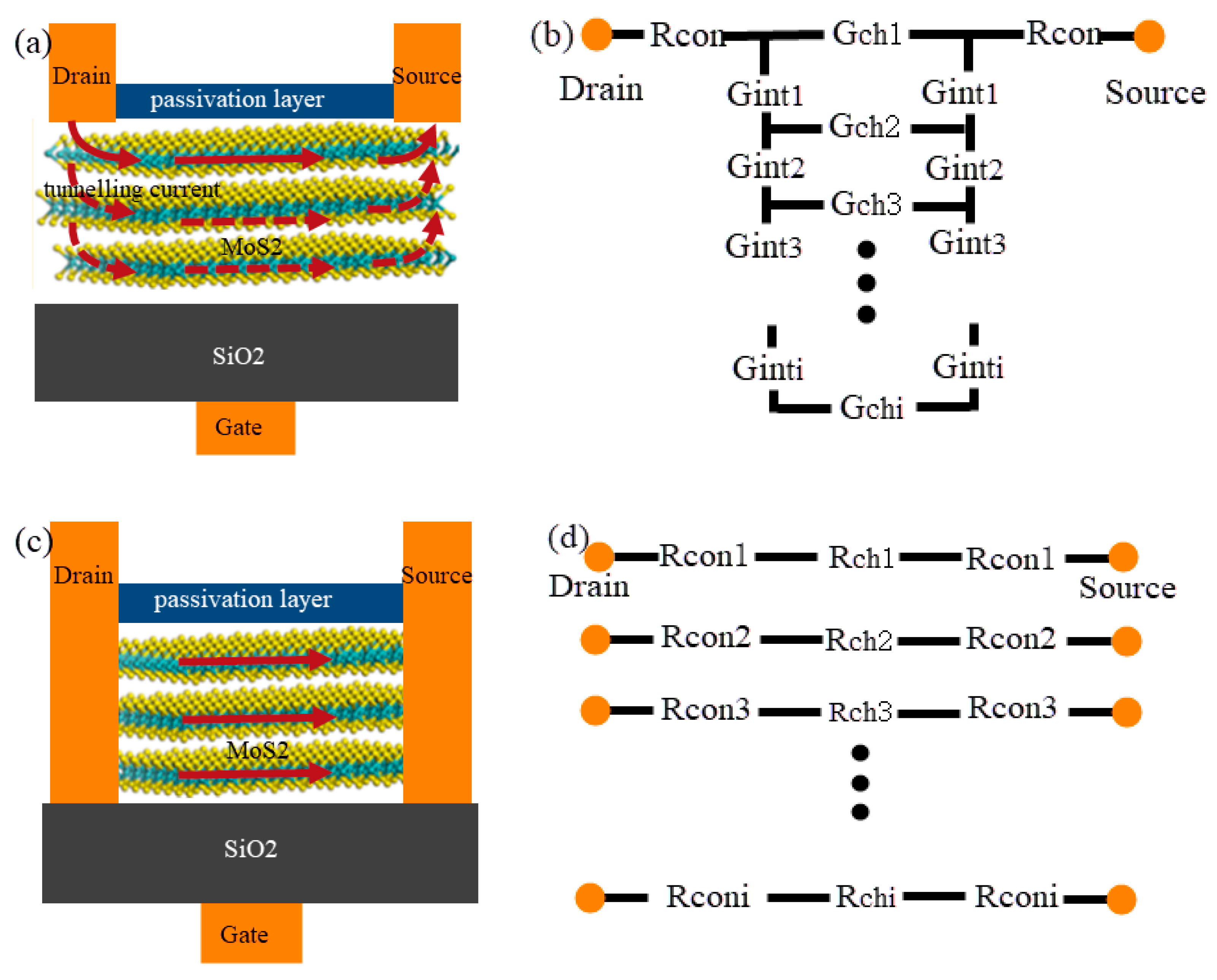
2. Fabrication
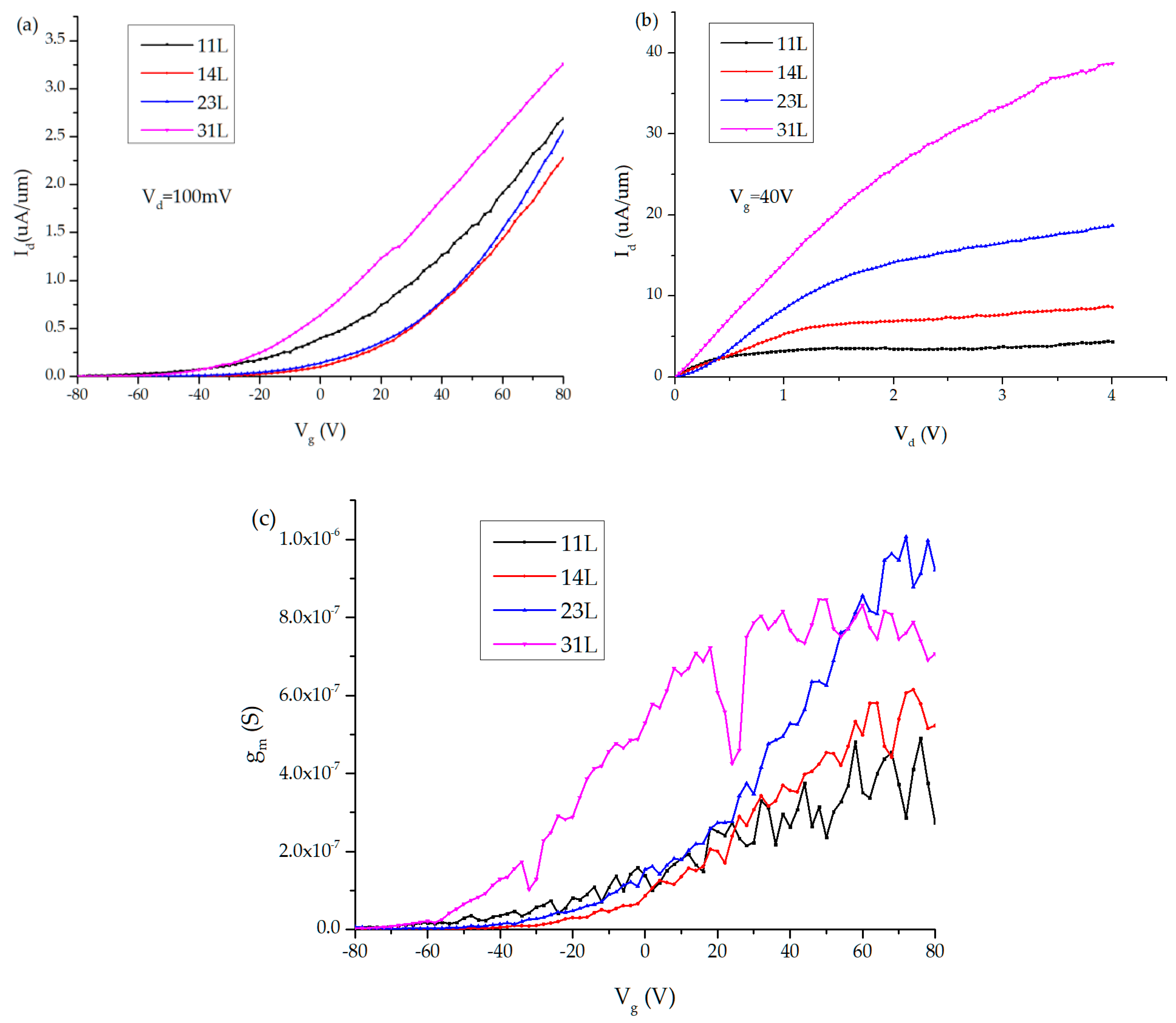
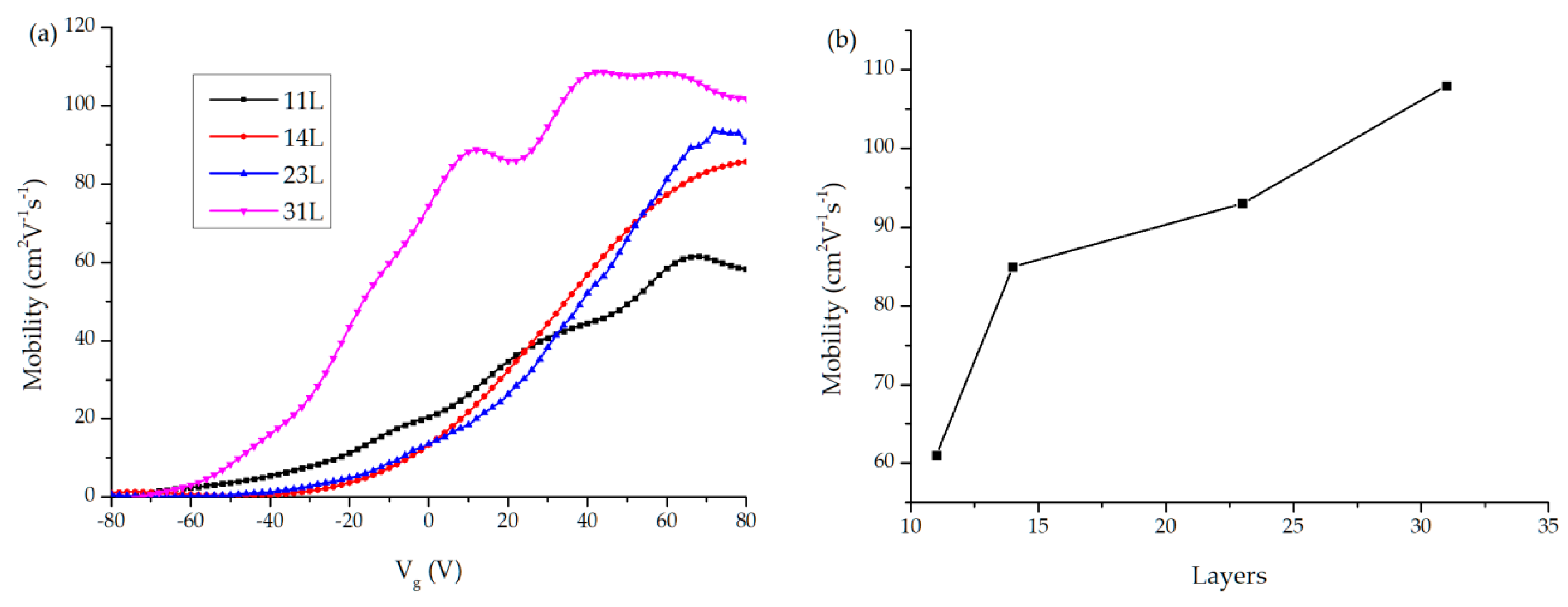
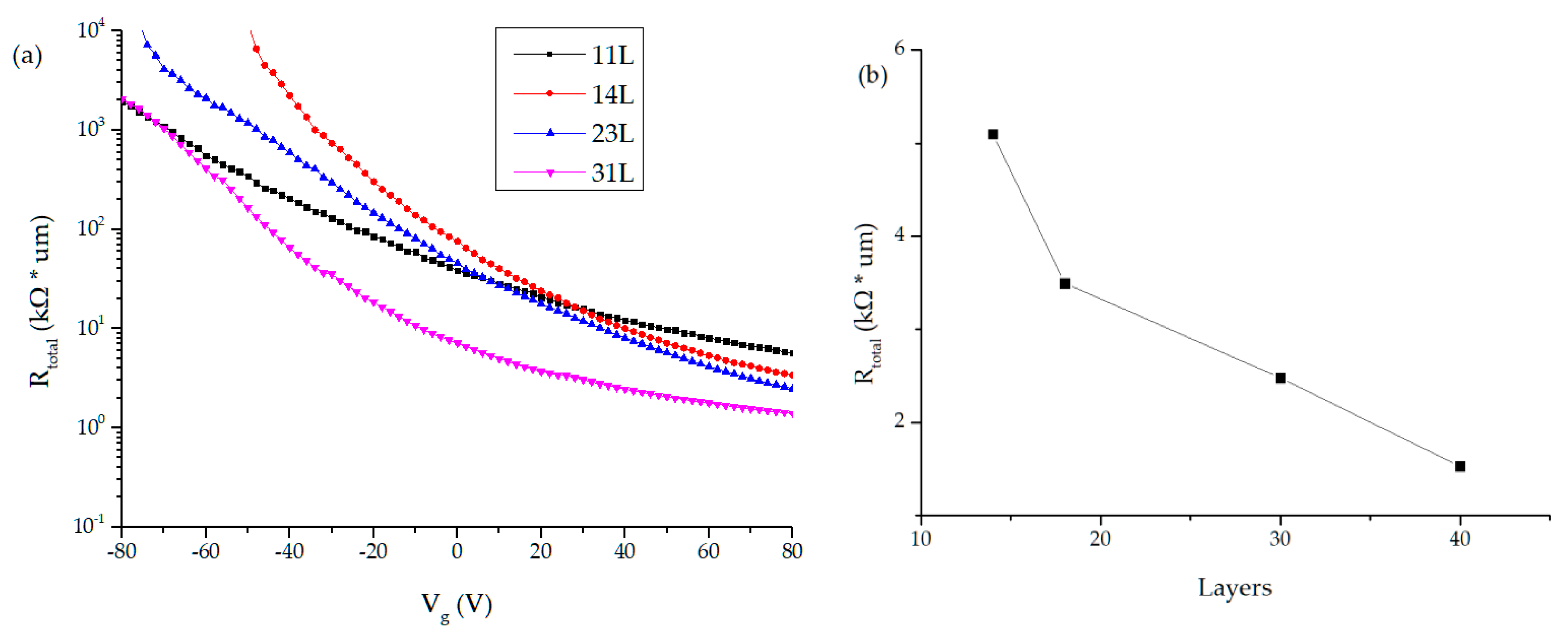
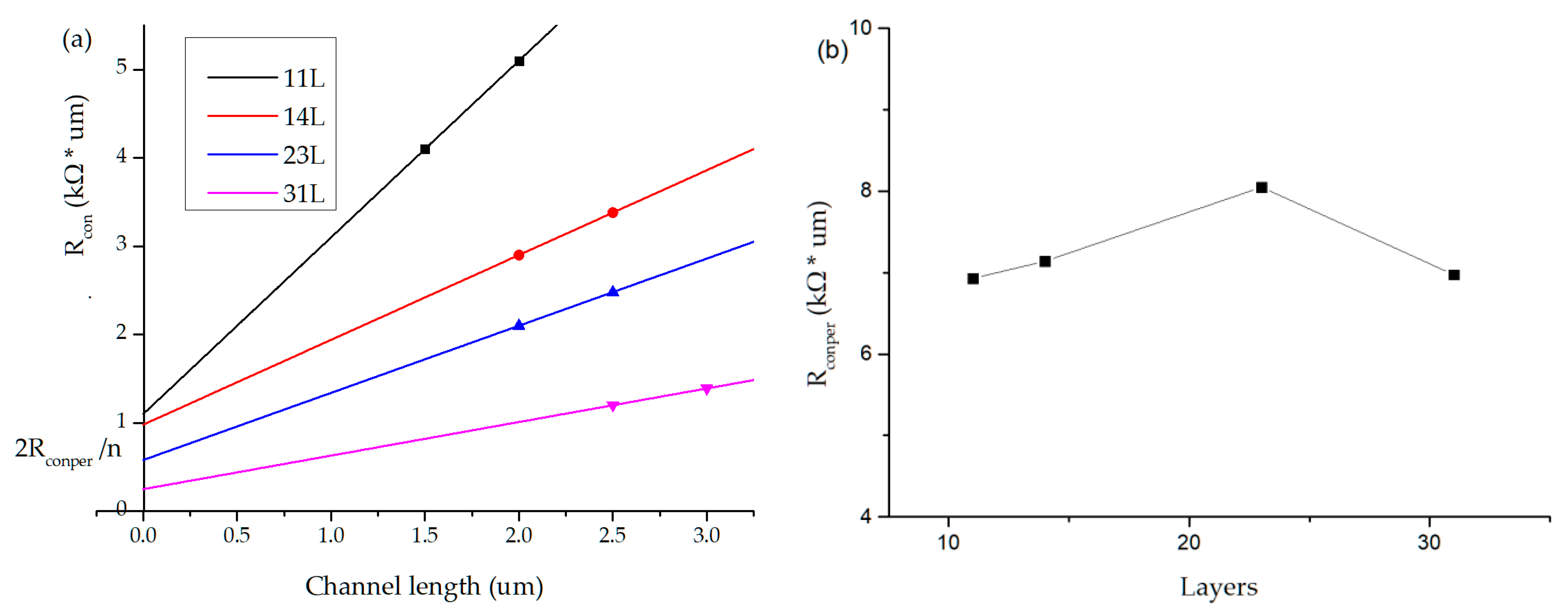
3. Results and Discussion
4. Conclusions
Author Contributions
Funding
Acknowledgments
Conflicts of Interest
References
- Mas-Ballesté, R.; Gómez-Navarro, C.; Gómez-Herrero, J.; Zamora, F. 2D materials: To graphene and beyond. Nanoscale 2011, 3, 20–30. [Google Scholar] [CrossRef]
- Gupta, A.; Sakthivel, T.; Seal, S. Recent development in 2D materials beyond graphene. Prog. Mater. Sci. 2015, 73, 44–126. [Google Scholar] [CrossRef]
- Novoselov, K.S.; Mishchenko, A.; Carvalho, A.; Neto, A.H.C. 2D materials and van der Waals heterostructures. Science 2016, 353. [Google Scholar] [CrossRef]
- Glavin, N.R.; Rao, R.; Varshney, V.; Bianco, E.; Apte, A.; Roy, A.; Ringe, E.; Ajayan, P.M. Emerging applications of elemental 2D materials. Adv. Mater. 2020, 32, 1904302. [Google Scholar] [CrossRef]
- Yin, Z.; Li, H.; Li, H.; Jiang, L.; Shi, Y.; Sun, Y.; Zhang, H. Single-layer MoS2 phototransistors. ACS Nano 2012, 6, 74–80. [Google Scholar] [CrossRef]
- Liu, L.; Park, J.; Siegel, D.A.; McCarty, K.F.; Clark, K.W.; Deng, W.; Gu, G. Heteroepitaxial growth of two-dimensional hexagonal boron nitride templated by graphene edges. Science 2014, 343, 163–167. [Google Scholar] [CrossRef] [PubMed]
- Choi, W.; Choudhary, N.; Han, G.H.; Park, J.; Akinwande, D.; Lee, Y.H. Recent development of two-dimensional transition metal dichalcogenides and their applications. Mater. Today 2017, 20, 116–130. [Google Scholar] [CrossRef]
- Liu, W.; Liu, M.; Liu, X.; Wang, X.; Deng, H.X.; Lei, M.; Wei, Z. Recent advances of 2D materials in nonlinear photonics and fiber lasers. Adv. Opt. Mater. 2020, 8, 1901631. [Google Scholar] [CrossRef]
- Shukla, V. Computational Studies of 2D Materials: Application to Energy Storage and Electron. Transport. in Nanoscale Devices. Ph. D. Thesis, Acta Universitatis Upsaliensis, Uppsala, Sweden, 1 March 2019. [Google Scholar]
- Akinwande, D.; Brennan, C.J.; Bunch, J.S.; Egberts, P.; Felts, J.R.; Gao, H.; Liechti, K.M. A review on mechanics and mechanical properties of 2D materials—Graphene and beyond. Extreme Mech. Lett. 2017, 13, 42–77. [Google Scholar] [CrossRef]
- Das, S.; Appenzeller, J. Where does the current flow in two-dimensional layered systems? Nano Lett. 2013, 13, 3396–3402. [Google Scholar] [CrossRef]
- Chu, T.; Chen, Z. Understanding the electrical impact of edge contacts in few-layer graphene. ACS Nano 2014, 8, 3584–3589. [Google Scholar] [CrossRef] [PubMed]
- Zhang, P.; Zhang, Y.; Wei, Y.; Jiang, H.; Wang, X.; Gong, Y. Contact engineering for two-dimensional semiconductors. J. Semicond. 2020, 41, 1–16. [Google Scholar] [CrossRef]
- Liu, W.; Zhang, A.; Zhang, Y.; Wang, Z.L. Density functional studies on edge-contacted single-layer MoS2 piezotronic transistors. Appl. Phys. Lett. 2015, 107, 083105. [Google Scholar] [CrossRef]
- Calado, V.E.; Goswami, S.; Nanda, G.; Diez, M.; Akhmerov, A.R.; Watanabe, K.; Vandersypen, L.M. Ballistic Josephson junctions in edge-contacted graphene. Nat. Nanotechnol. 2015, 10, 761–764. [Google Scholar] [CrossRef]
- Wang, L.; Meric, I.; Huang, P.Y.; Gao, Q.; Gao, Y.; Tran, H.; Guo, J. One-dimensional electrical contact to a two-dimensional material. Science 2013, 342, 614–617. [Google Scholar] [CrossRef]
- Galiy, P.V.; Randle, M.; Lipatov, A.; Wang, L.; Gilbert, S.; Vorobeva, N.; Yin, S. Building the quasi one dimensional transistor from 2D materials. In Proceedings of the 2019 IEEE 2nd Ukraine Conference on Electrical and Computer Engineering (UKRCON), Lviv, Ukraine, 2–6 July 2019; pp. 679–682. [Google Scholar]
- Wang, L.; Chen, Z.; Dean, C.R.; Taniguchi, T.; Watanabe, K.; Brus, L.E.; Hone, J. Negligible environmental sensitivity of graphene in a hexagonal boron nitride/graphene/h-BN sandwich structure. ACS Nano 2012, 6, 9314–9319. [Google Scholar] [CrossRef]
- Liu, W.; Kang, J.; Cao, W.; Sarkar, D.; Khatami, Y.; Jena, D.; Banerjee, K. High-performance few-layer-MoS 2 field-effect-transistor with record low contact-resistance. In Proceedings of the 2013 IEEE International Electron. Devices Meeting, Washington, DC, USA, 9–11 December 2013; pp. 19.4.1–19.4.4. [Google Scholar]
- Kim, S.Y.; Park, S.; Choi, W. Enhanced carrier mobility of multilayer MoS2 thin-film transistors by Al2O3 encapsulation. Appl. Phys. Lett. 2016, 109, 152101. [Google Scholar] [CrossRef]
- Chee, S.S.; Seo, D.; Kim, H.; Jang, H.; Lee, S.; Moon, S.P.; Ham, M.H. Lowering the Schottky Barrier Height by Graphene/Ag Electrodes for High-Mobility MoS2 Field-Effect Transistors. Adv. Mater. 2019, 31, 1804422. [Google Scholar] [CrossRef] [PubMed]
- Jiang, J.; Zhang, Y.; Wang, A.; Duan, J.; Ji, H.; Pang, J.; Han, L. Construction of High Field-Effect Mobility Multilayer MoS2 Field-Effect Transistors with Excellent Stability through Interface Engineering. ACS Appl. Electron. Mater. 2020, 2, 2132–2140. [Google Scholar] [CrossRef]
- Nagashio, K.; Nishimura, T.; Kita, K.; Toriumi, A. Contact resistivity and current flow path at metal/graphene contact. Appl. Phys. Lett. 2010, 97, 143514. [Google Scholar] [CrossRef]
- Matsuda, Y.; Deng, W.Q.; Goddard, W.A., III. Contact resistance for “end-contacted” metal− graphene and metal− nanotube interfaces from quantum mechanics. J. Phys. Chem. C 2010, 114, 17845–17850. [Google Scholar] [CrossRef]
- Venugopal, A.; Colombo, L.; Vogel, E.M. Contact resistance in few and multilayer graphene devices. Appl. Phys. Lett. 2010, 96, 13512. [Google Scholar] [CrossRef]
- Pacheco-Sanchez, A.; Jimenez, D. Efficient contact resistance extraction from individual device characteristics of graphene FETs. In Proceedings of the 2019 IEEE 14th Nanotechnology Materials and Devices Conference (NMDC), Stockholm, Sweden, 27–30 October 2019; pp. 1–4. [Google Scholar]
- Luo, S.; Lam, K.T.; Wang, B.; Hsu, C.H.; Huang, W.; Yao, L.Z.; Liang, G. Effects of contact placement and Intra/Interlayer interaction in current distribution of black phosphorus Sub-10-nm FET. IEEE Transact. Electron. Devices 2016, 64, 579–586. [Google Scholar] [CrossRef]
- Jang, J.; Kim, Y.; Chee, S.S.; Kim, H.; Whang, D.; Kim, G.H.; Yun, S.J. Clean Interface Contact Using a ZnO Interlayer for Low-Contact-Resistance MoS2 Transistors. ACS Appl. Mater. Interfaces 2019, 12, 5031–5039. [Google Scholar] [CrossRef]
- Walter, T.N.; Cooley, K.A.; Domask, A.C.; Mohney, S.E. Nickel diffusion into MoS2 and the effect of annealing on contact resistance. Mater. Sci. Semicond. Process. 2020, 107, 104850. [Google Scholar] [CrossRef]
- English, C.D.; Shine, G.; Dorgan, V.E.; Saraswat, K.C.; Pop, E. Improved contacts to MoS2 transistors by ultra-high vacuum metal deposition. Nano Lett. 2016, 16, 3824–3830. [Google Scholar] [CrossRef]


| Paper | Channel Thickness | Mobility (cm2/Vs) | Electrode Structure |
|---|---|---|---|
| [19] | 8 L | 54 | edge |
| [20] | multilayer | 71.8 | combined |
| [21] | 1 L | 35 | top |
| [22] | 30 nm | 104 | edge |
| This work | 31 L | 107 | edge |
| Layers | Rcon (kΩ∙um) |
|---|---|
| 11 | 0.632 |
| 14 | 0.511 |
| 23 | 0.350 |
| 31 | 0.225 |
Publisher’s Note: MDPI stays neutral with regard to jurisdictional claims in published maps and institutional affiliations. |
© 2020 by the authors. Licensee MDPI, Basel, Switzerland. This article is an open access article distributed under the terms and conditions of the Creative Commons Attribution (CC BY) license (http://creativecommons.org/licenses/by/4.0/).
Share and Cite
Cai, F.; Deng, G.; Li, X.; Lin, F. Contact Resistance Parallel Model for Edge-Contacted 2D Material Back-Gate FET. Electronics 2020, 9, 2110. https://doi.org/10.3390/electronics9122110
Cai F, Deng G, Li X, Lin F. Contact Resistance Parallel Model for Edge-Contacted 2D Material Back-Gate FET. Electronics. 2020; 9(12):2110. https://doi.org/10.3390/electronics9122110
Chicago/Turabian StyleCai, Fei, Guangsheng Deng, Xiangxiang Li, and Fujiang Lin. 2020. "Contact Resistance Parallel Model for Edge-Contacted 2D Material Back-Gate FET" Electronics 9, no. 12: 2110. https://doi.org/10.3390/electronics9122110
APA StyleCai, F., Deng, G., Li, X., & Lin, F. (2020). Contact Resistance Parallel Model for Edge-Contacted 2D Material Back-Gate FET. Electronics, 9(12), 2110. https://doi.org/10.3390/electronics9122110