Resistive Switching in Non-Stoichiometric Germanosilicate Glass Films Containing Ge Nanoclusters

 ,
,  , ,
, ,
Abstract
1. Introduction
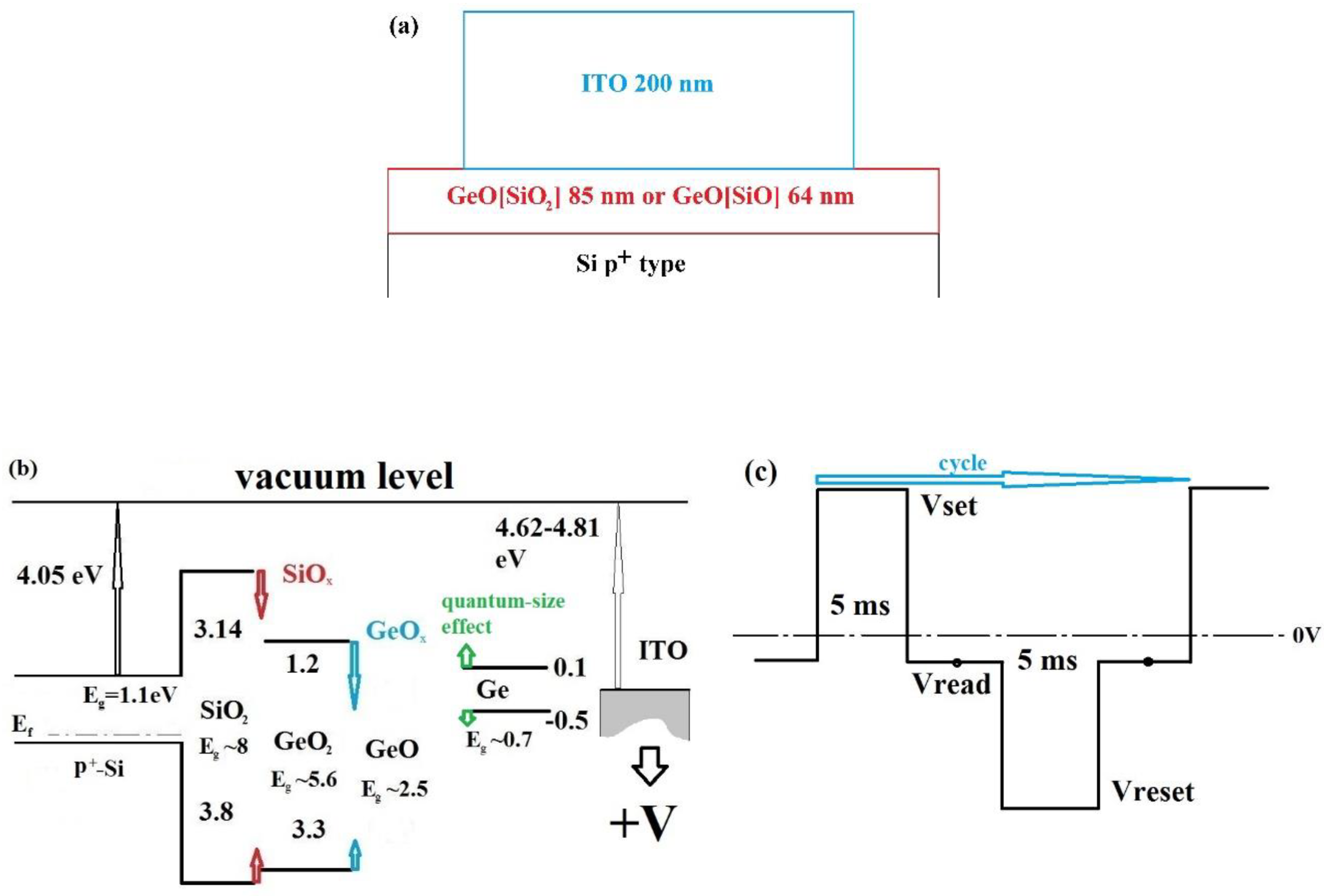
2. Experiment
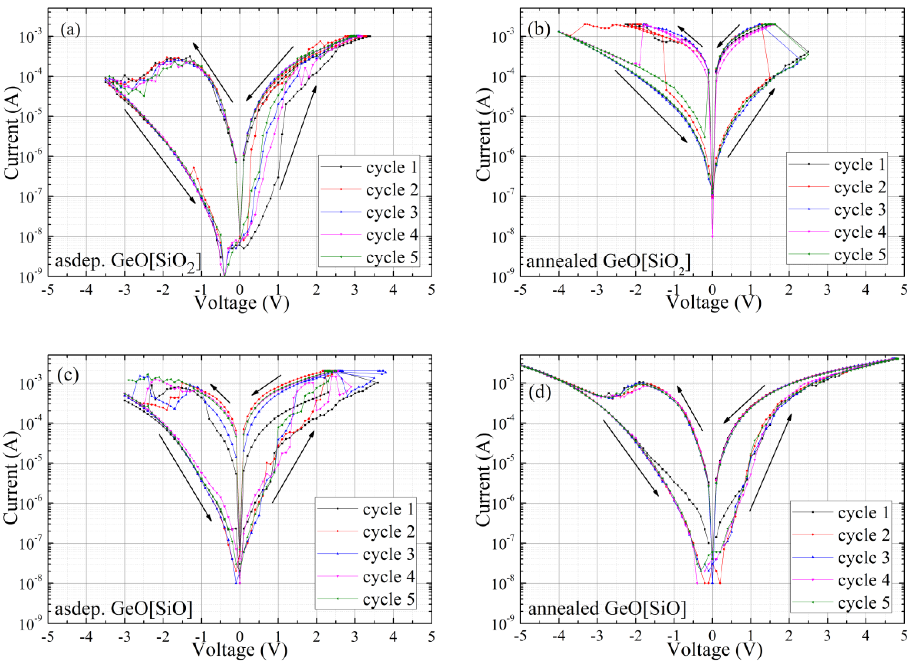
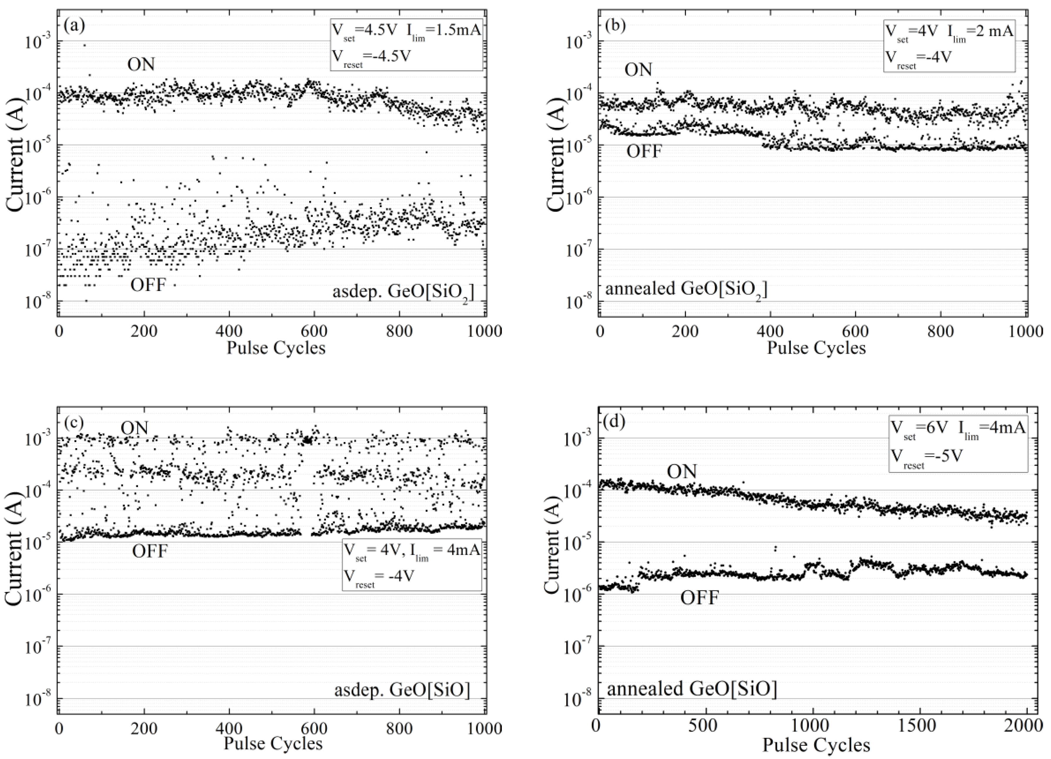
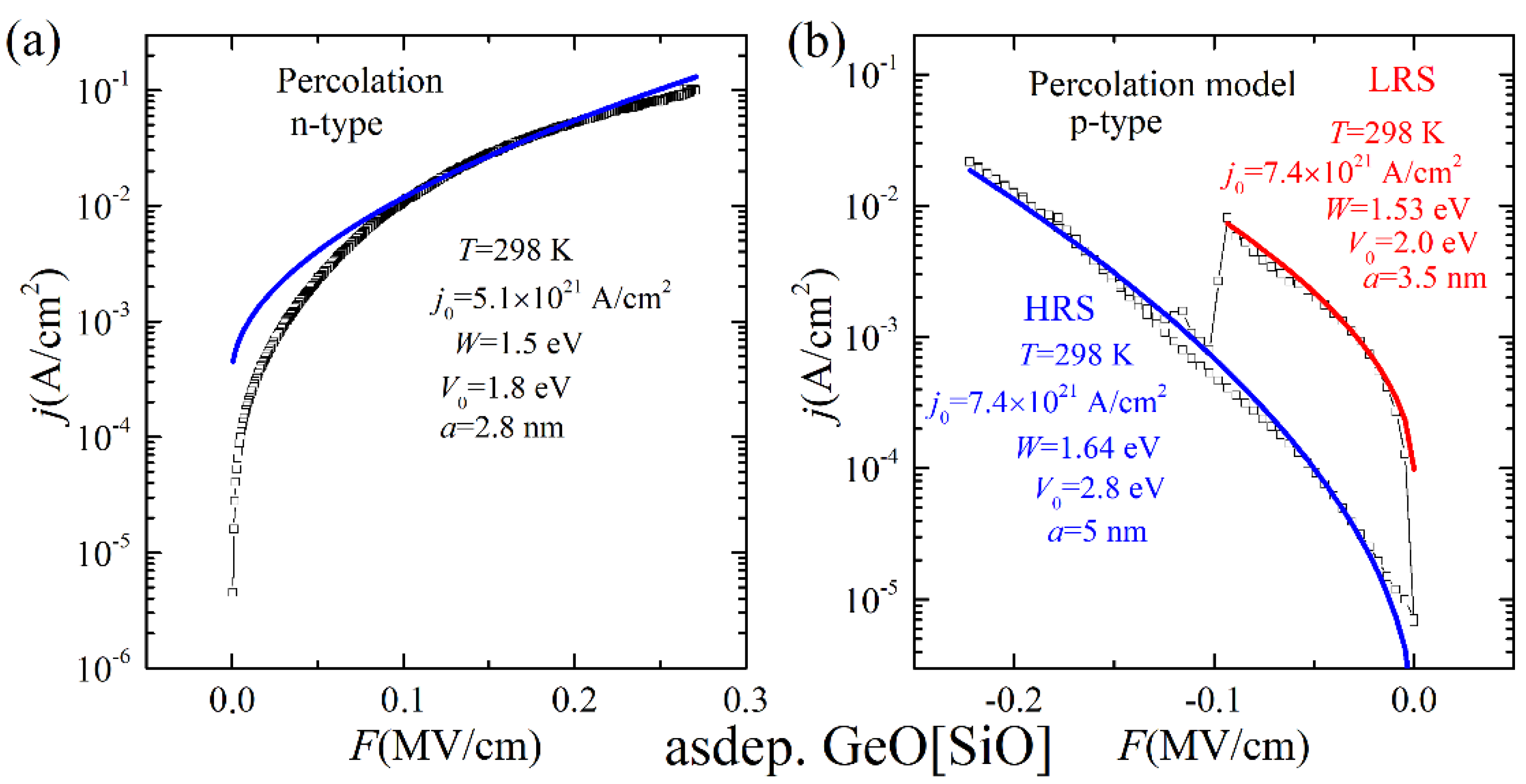
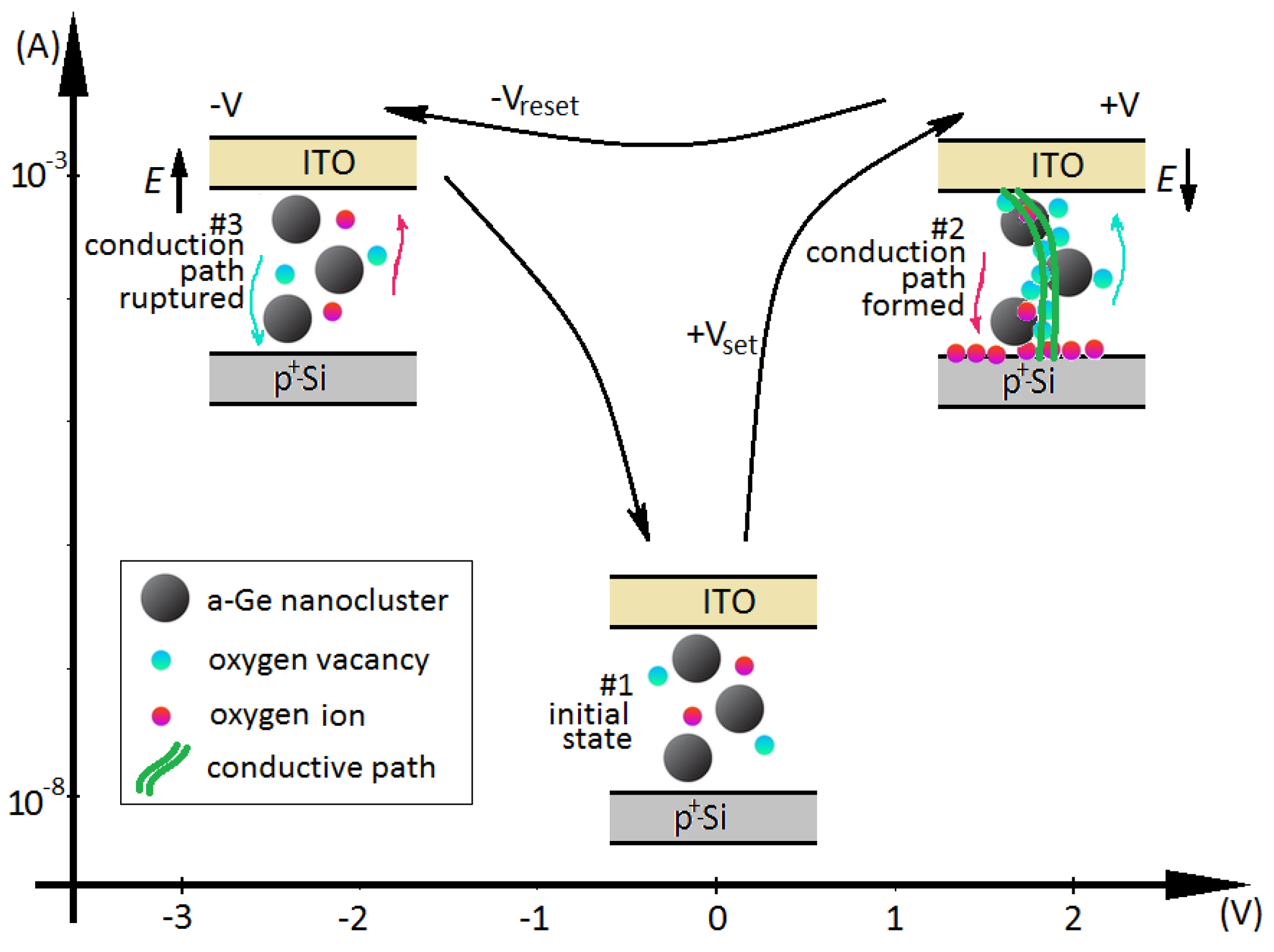
3. Results and Discussion
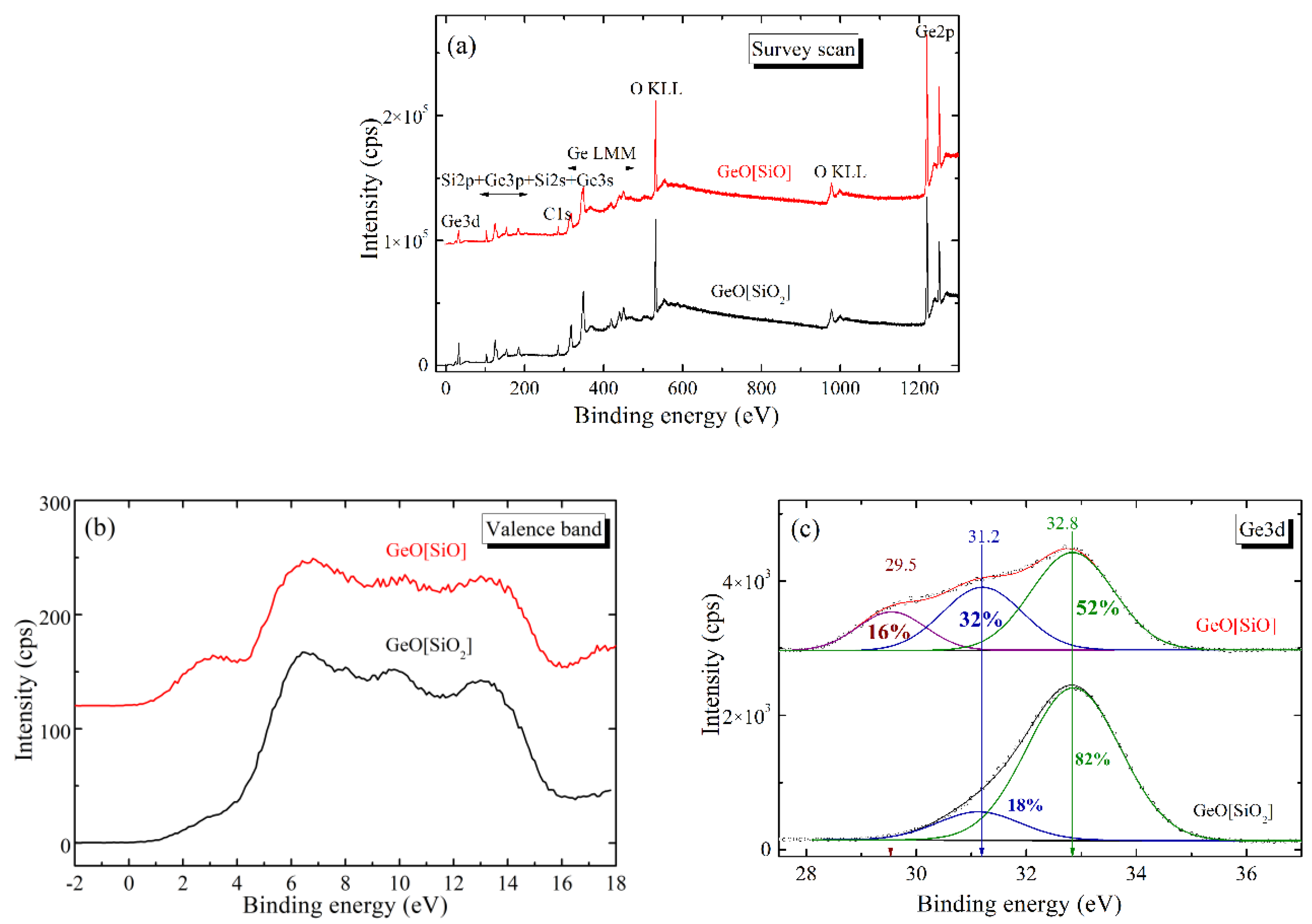
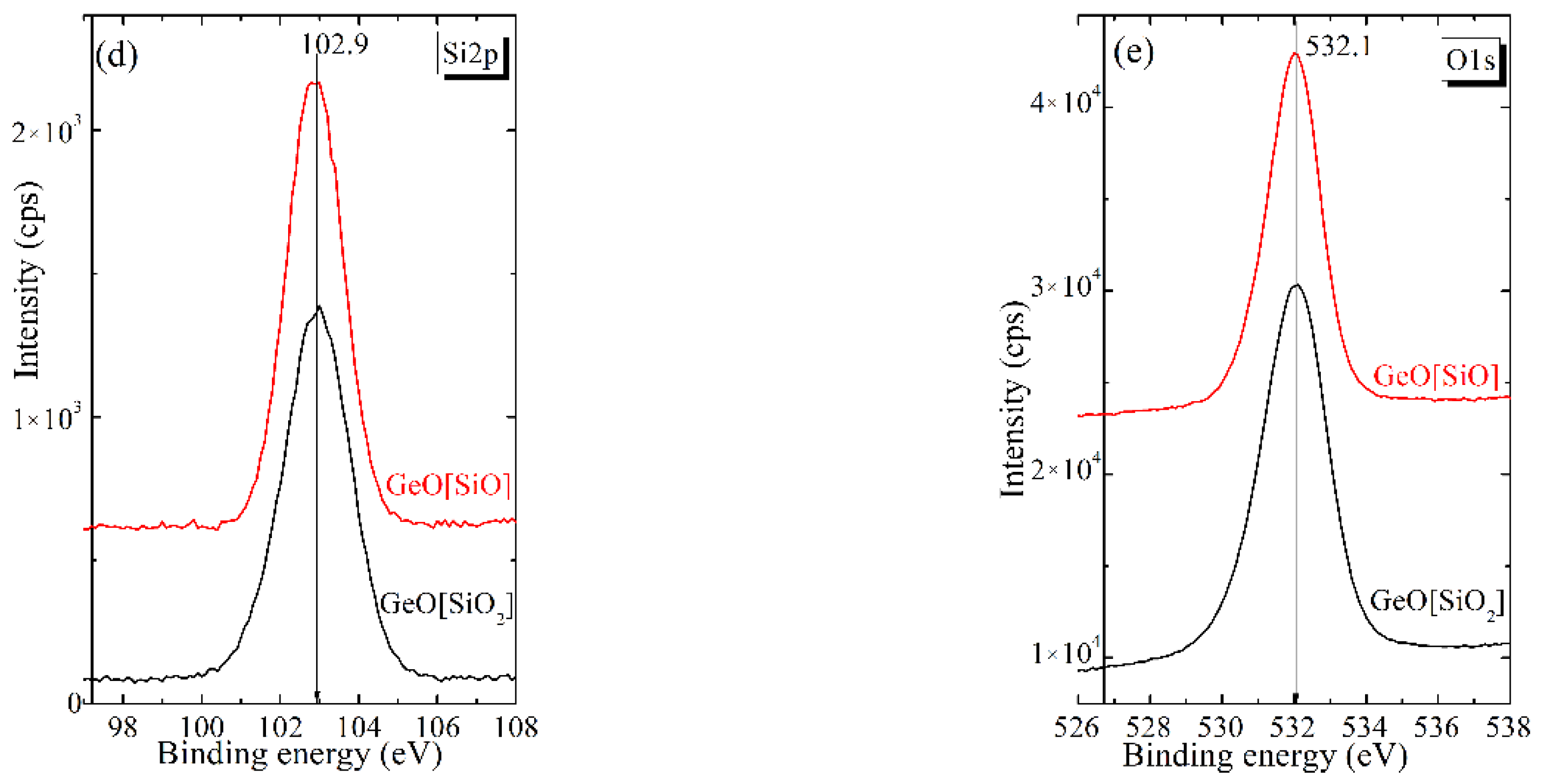
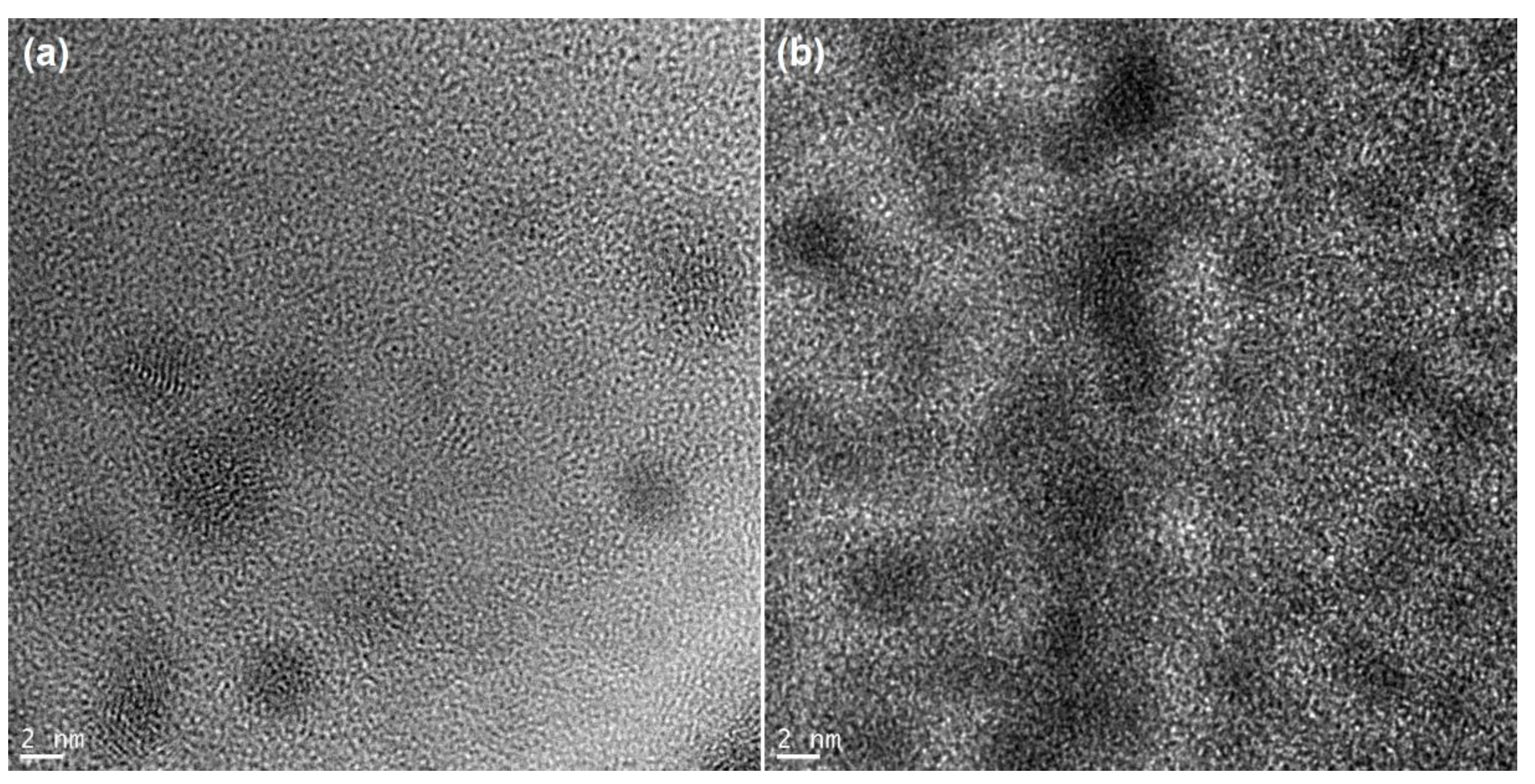
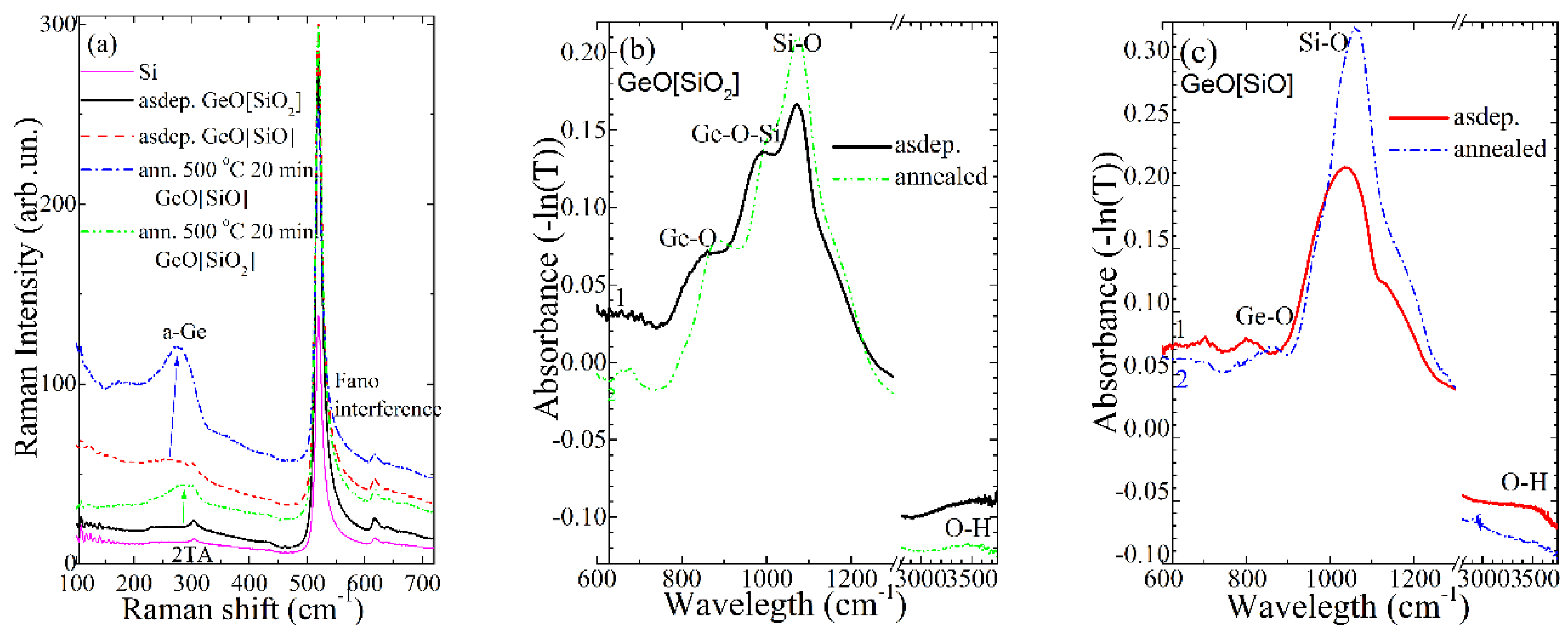
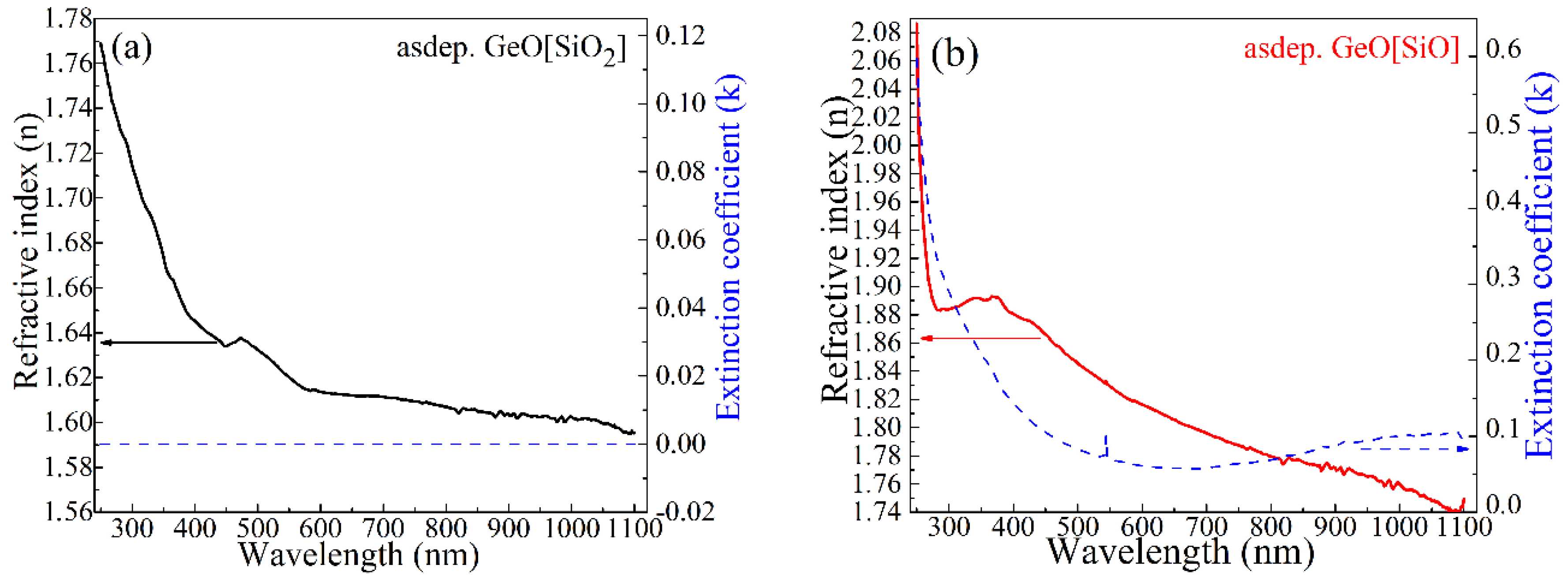
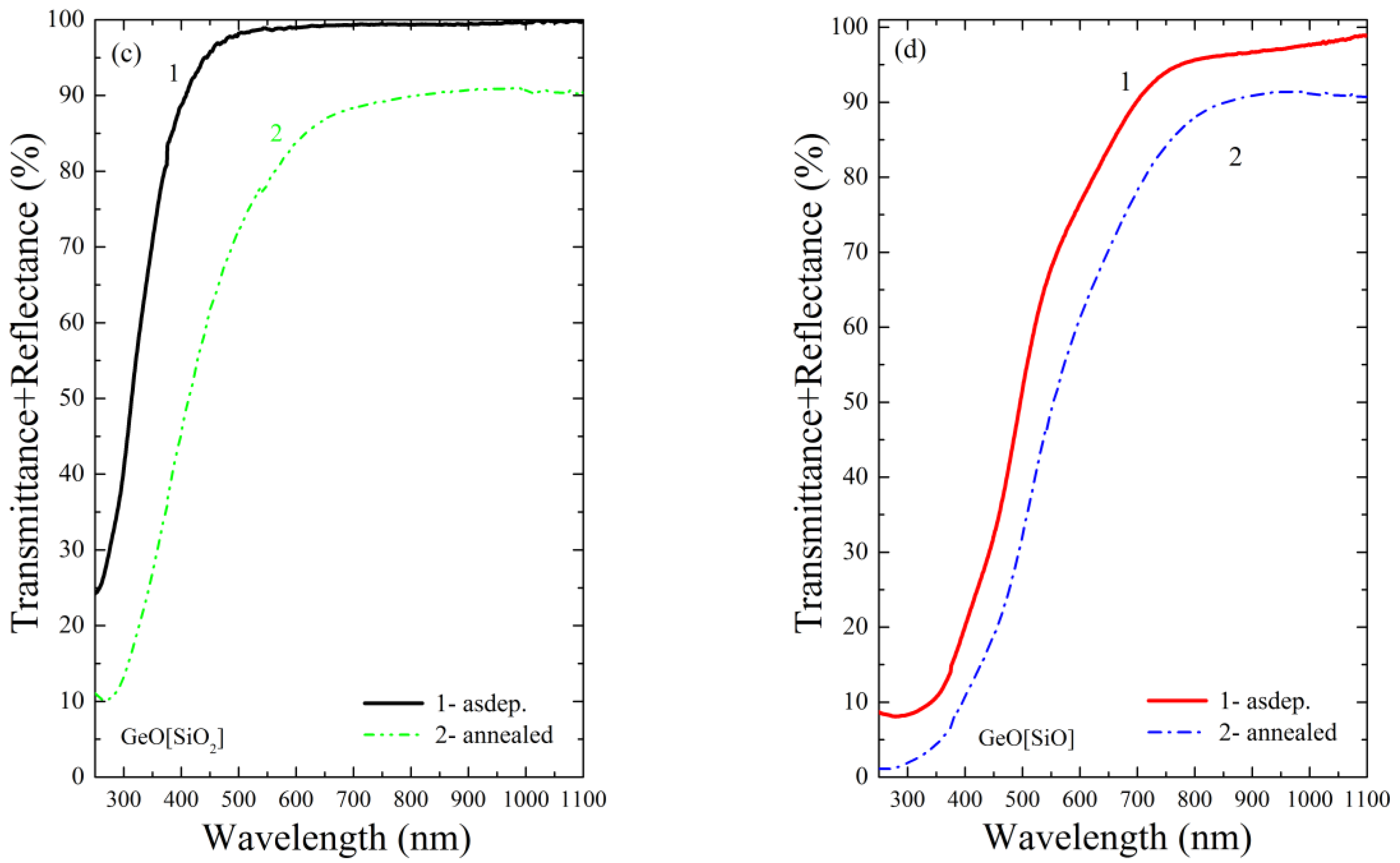
3.1. Structural Studies
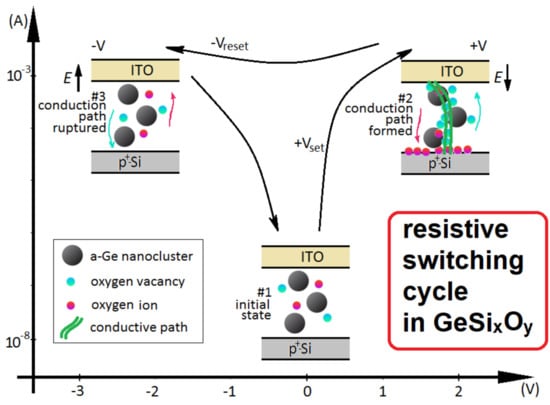
3.2. Studies of Resistivity Switching and Endurance
4. Conclusions
Supplementary Materials
Author Contributions
Funding
Acknowledgments
Conflicts of Interest
References
- Zidan, M.A.; Strachan, J.P.; Lu, W.D. The future of electronics based on memristive systems. Nat. Electron. 2018, 1, 22. [Google Scholar] [CrossRef]
- Chua, L.O.; Kang, S.M. Memristive devices and systems. Proc. IEEE 1976, 64, 2. [Google Scholar] [CrossRef]
- Strukov, D.B.; Snider, G.S.; Stewart, D.R.; Stanley Williams, R. The missing memristor found. Nature 2008, 453, 80. [Google Scholar] [CrossRef] [PubMed]
- Terai, M.; Sakotsubo, Y.; Kotsuji, S.; Hada, H. Resistance Controllability of Ta2O5/TiO2 Stack ReRAM for Low-Voltage and Multilevel Operation. IEEE Electron. Device Lett. 2010, 31, 204. [Google Scholar] [CrossRef]
- Yan, K.; Peng, M.; Yu, X.; Cai, X.; Chen, S.; Hu, H.; Chen, B.; Gao, X.; Dong, B.; Zou, D. High-performance perovskite memristor based on methyl ammonium lead halides. J. Mater. Chem. C 2016, 4, 1375. [Google Scholar] [CrossRef]
- Battistoni, S.; Erokhin, V.; Iannotta, S. Organic memristive devices for perceptron applications. J. Phys. D Appl. Phys. 2018, 51, 284002. [Google Scholar] [CrossRef]
- Romero, F.J.; Toral, A.; Medina-Rull, A.; Moraila-Martinez, C.L.; Morales, D.P.; Ohata, A.; Godoy, A.; Ruiz, F.G.; Rodriguez, N. Resistive Switching in Graphene Oxide. Front. Mater. 2020, 7, 17. [Google Scholar] [CrossRef]
- Lee, H.Y.; Chen, P.S.; Wu, T.Y.; Wang, C.C.; Tzeng, P.J.; Lin, C.H.; Chen, F.; Tsai, M.-J. Low power and high speed bipolar switching with a thin reactive Ti buffer layer in robust HfO2 based RRAM. In Proceedings of the IEEE International Electron Devices Meeting, San Francisco, CA, USA, 15–17 December 2008. [Google Scholar]
- Wei, Z.; Kanzawa, Y.; Arita, K.; Katoh, Y.; Kawai, K.; Muraoka, S.; Mitani, S.; Fujii, S.; Katayama, K.; Iijima, M.; et al. Highly reliable TaOx ReRAM and direct evidence of redox reaction mechanism. In Proceedings of the IEEE International Electron Devices Meeting, San Francisco, CA, USA, 15–17 December 2008. [Google Scholar]
- Lee, M.J.; Lee, C.B.; Lee, D.; Lee, S.R.; Chang, M.; Hur, J.H.; Kim, Y.B.; Kim, C.J.; Seo, D.H.; Seo, S.; et al. A fast, high-endurance and scalable non-volatile memory device made from asymmetric Ta2O(5−x)/TaO(2−x) bilayer structures. Nat. Mater. 2011, 10, 625. [Google Scholar] [CrossRef]
- Shaposhnikov, A.V.; Perevalov, T.V.; Gritsenko, V.A.; Cheng, C.H.; Chin, A. Mechanism of GeO2 resistive switching based on the multi-phonon assisted tunneling between traps. Appl. Phys. Lett. 2012, 100, 243506. [Google Scholar] [CrossRef]
- Yen, T.J.; Chin, A.; Gritsenko, V. High Performance All Nonmetal SiNx Resistive Random Access Memory with Strong Process Dependence. Sci. Rep. 2020, 10, 2807. [Google Scholar] [CrossRef]
- Zackriya, M.; Kittur, H.M.; Chin, A. A Novel Read Scheme for Large Size One-Resistor Resistive Random Access Memory Array. Sci. Rep. 2017, 7, 42375. [Google Scholar] [CrossRef] [PubMed]
- Mehonic, A.; Shluger, A.L.; Gao, D.; Valov, I.; Miranda, E.; Ielmini, D.; Bricalli, A.; Ambrosi, E.; Li, C.; Yang, J.J.; et al. Silicon Oxide (SiOx): A Promising Material for Resistance Switching? Adv. Mater. 2018, 30, 1801187. [Google Scholar] [CrossRef] [PubMed]
- Kawauchi, T.; Kano, S.; Fujii, M. Forming-free resistive switching in solution-processed silicon nanocrystal thin film. J. Appl. Phys. 2018, 124, 085113. [Google Scholar] [CrossRef]
- Fan, J.; Kapur, O.; Huang, R.; King, S.W.; de Groot, C.H.; Jiang, L. Back-end-of-line a-SiOxCy:H dielectrics for resistive memory. AIP Adv. 2018, 8, 095215. [Google Scholar] [CrossRef]
- Yen, T.J.; Gismatulin, A.; Volodin, V.; Gritsenko, V.; Chin, A. All Nonmetal Resistive Random Access Memory. Sci. Rep. 2019, 9, 6144. [Google Scholar] [CrossRef]
- Volodin, V.A.; Kamaev, G.N.; Gritsenko, V.A.; Gismatulin, A.A.; Chin, A.; Vergnat, M. Memristor effect in GeO[SiO2] and GeO[SiO] solid alloys films. Appl. Phys. Lett. 2019, 114, 233104. [Google Scholar] [CrossRef]
- Hwang, H.G.; Woo, J.U.; Lee, T.H.; Park, S.M.; Lee, T.G.; Lee, W.H.; Nahm, S. Synaptic plasticity and preliminary-spike-enhanced plasticity in a CMOS-compatible Ta2O5 memristor. Mater. Des. 2020, 187, 108400. [Google Scholar] [CrossRef]
- Wang, R.; Shi, T.; Zhang, X.; Wang, W.; Wei, J.; Lu, J.; Zhao, X.; Wu, Z.; Cao, R.; Long, S.; et al. Bipolar analog Memristors as artificial synapses for neuromorphic computing. Materials 2018, 11, 2102. [Google Scholar] [CrossRef]
- Ardyanian, M.; Rinnert, H.; Devaux, X.; Vergnat, M. Structure and photoluminescence properties of evaporated GeOx thin films. Appl. Phys. Lett. 2006, 89, 011902. [Google Scholar] [CrossRef]
- Marin, D.V.; Volodin, V.A.; Gorokhov, E.B.; Shcheglov, D.V.; Latyshev, A.V.; Vergnat, M.; Koch, J.; Chichkov, B.N. Modification of germanium nanoclusters in GeOx films during isochronous furnace and pulse laser annealing. Appl. Phys. Lett. 2010, 36, 439. [Google Scholar]
- Moulder, J.F.; Stickle, W.F.; Sobol, P.E.; Bomben, K.D. Handbook of X-ray Photoelectron Spectroscopy; Chastain, J., Ed.; Perkin-Elmer: Eden Prairie, MN, USA, 1992; p. 190. [Google Scholar]
- Gritsenko, V.A.; Kruchinin, V.N.; Prosvirin, I.P.; Novikov, Y.N.; Chin, A.; Volodin, V.A. Atomic and Electronic Structures of a-SiNx:H. J. Exp. Theor. 2019, 129, 924. [Google Scholar] [CrossRef]
- Zhigunov, D.M.; Kamaev, G.N.; Kashkarov, P.K.; Volodin, V.A. On Raman scattering cross section ratio of crystalline and microcrystalline to amorphous silicon. Appl. Phys. Lett. 2018, 113, 023101. [Google Scholar] [CrossRef]
- Fan, Z.; Kochubey, S.A.; Stoffel, M.; Rinnert, H.; Vergnat, M.; Volodin, V.A. On the Formation of Amorphous Ge Nanoclusters and Ge Nanocrystals in GeSixOy Films on Quartz Substrates by Furnace and Pulsed Laser Annealing. Semiconductors 2020, 54, 322. [Google Scholar]
- Scofield, J.H. Hartree-Slater subshell photoionization cross-sections at 1254 and 1487 eV. J. Electron. Spectros. Relat. Phenom. 1976, 8, 129. [Google Scholar] [CrossRef]
- Kalimuthu, V.; Kumar, P.; Kumar, M.; Rath, S. Growth mechanism and optical properties of Ge nanocrystals embedded in a GeOx matrix. Appl. Phys. A 2018, 124, 712. [Google Scholar] [CrossRef]
- Tabet, N.; Faiz, M.; Hamdan, N.M.; Hussain, Z. High resolution XPS study of oxide layers grown on Ge substrates. Surf. Sci. 2003, 523, 68. [Google Scholar] [CrossRef]
- Xpspeak Software Web Site. Available online: http://xpspeak.software.informer.com/4.1/ (accessed on 9 November 2020).
- Gambaryan, M.P.; Krivyakin, G.K.; Cherkova, S.G.; Stoffel, M.; Rinnert, H.; Vergnat, M.; Volodin, V.A. Quantum Size Effects in Germanium Nanocrystals and Amorphous Nanoclusters in GeSixOy Films. Phys. Solid State 2020, 62, 492. [Google Scholar] [CrossRef]
- Kolobov, A.V. Raman scattering from Ge nanostructures grown on Si substrates: Power and limitations. J. Appl. Phys. 2000, 87, 2926. [Google Scholar] [CrossRef]
- Cerdeira, F.; Fjeldly, T.A.; Cardona, M. Raman study of the interaction between localized vibrations and electronic excitations in boron-doped silicon. Phys. Rev. B 1974, 9, 4344. [Google Scholar] [CrossRef]
- Wihl, M.; Cardona, M.; Tauc, J. Raman scattering in amorphous Ge and III–V compounds. J. Non-Cryst. Solids 1972, 8–10, 172–178. [Google Scholar] [CrossRef]
- Volodin, V.A.; Kamaev, G.N.; Vergnat, M. Negative and Positive Photoconductivity and Memristor Effect in Alloyed GeO[SiO] Films Containing Ge Nanoclusters. Phys. Stat. Sol. (RRL) 2020, 14, 2000165. [Google Scholar] [CrossRef]
- Gorokhov, E.B.; Volodin, V.A.; Marin, D.V.; Orekhov, D.A.; Cherkov, A.G.; Gutakovskii, A.K.; Shwets, V.A.; Borisov, A.G.; Efremov, M.D. Effect of quantum confinement on optical properties of Ge nanocrystals in GeO2 films. Semiconductors 2005, 39, 1168. [Google Scholar] [CrossRef]
- Lucovsky, G.; Yang, J.; Chao, S.S.; Tyler, J.E.; Czubatyj, W. Oxygen-bonding environments in glow-discharge-deposited amorphous silicon-hydrogen alloy films. Phys. Rev. B 1983, 28, 3225. [Google Scholar] [CrossRef]
- Pai, P.G.; Chao, S.S.; Takagi, Y.; Lucovsky, G. Infrared spectroscopic study of SiOx films produced by plasma enhanced chemical vapor deposition. J. Vac. Sci. Technol. A 1986, 4, 689. [Google Scholar] [CrossRef]
- Cherkova, S.G.; Volodin, V.A.; Skuratov, V.A.; Stoffel, M.; Rinnert, H.; Vergnat, M. Infrared photoluminescence from GeO[SiO2] and GeO[SiO] solid alloy layers irradiated with swift heavy Xe ions. J. Lumin. 2020, 223, 117238. [Google Scholar] [CrossRef]
- Seck, M.; Devine, R.A.B.; Hernandez, C.; Campidelli, Y.; Dupuy, J.C. Study of Ge bonding and distribution in plasma oxides of Si1−xGex alloys. Appl. Phys. Lett. 1998, 72, 2748. [Google Scholar] [CrossRef]
- Shabalov, A.L.; Feldman, M.S. Optical properties of thin GeOx films. Phys. Status Solidi A 1984, 83, K11. [Google Scholar] [CrossRef]
- Jishiashvili, D.A.; Kutelia, E.R. Infrared Spectroscopic Study of GeOx Films. Phys. Status Solidi B 1987, 143, K147. [Google Scholar] [CrossRef]
- Perevalov, T.V.; Volodin, V.A.; Kamaev, G.N.; Krivyakin, G.K.; Gritsenko, V.A.; Prosvirin, I.P. Electronic structure and nanoscale potential fluctuations in strongly nonstoichiometric PECVD SiOx. J. Non-Cryst. Solids 2020, 529, 119796. [Google Scholar] [CrossRef]
- Tompkins, H.G.; Irene, E.A. Handbook of Ellipsometry; William Andrew Pub: Norwich, NY, USA, 2005. [Google Scholar]
- Marin, D.V.; Gorokhov, E.B.; Borisov, A.G.; Volodin, V.A. Ellipsometry of GeO2 films with Ge nanoclusters: Influence of the quantum-size effect on refractive index. Opt. Spectrosc. 2009, 106, 436. [Google Scholar] [CrossRef]
- Volodin, V.A.; Gambaryan, M.P.; Cherkov, A.G.; Stoffel, M.; Rinnert, H.; Vergnat, M. Structure and infrared photoluminescence of GeSi nanocrystals formed by high temperature annealing of GeOx/SiO2 multilayers. Mater. Res. Express 2016, 3, 085019. [Google Scholar] [CrossRef]
- Gritsenko, V.A.; Volodin, V.A.; Perevalov, T.V.; Kruchinin, V.N.; Gerasimova, A.K.; Aliev, V.S.; Prosvirin, I.P. Nanoscale potential fluctuations in nonstoichiometrics tantalum oxide. Nanotechnology 2018, 29, 425202. [Google Scholar] [CrossRef]
- Broqvist, P.; Binder, J.F.; Pasquarello, A. Band offsets at the Ge/GeO2 interface through hybrid density functionals. Appl. Phys. Lett. 2009, 94, 141911. [Google Scholar] [CrossRef]
- Tikhov, S.V.; Gorshkov, O.N.; Antonov, I.N.; Kasatkin, A.P.; Korolev, D.S.; Belov, A.I.; Mikhaylov, A.N.; Tetel’baum, D.I. Change of immitance during electroforming and resistive switching in the metal-insulator-metal memristive structures based on SiOx. Tech. Phys. 2016, 61, 745–749. [Google Scholar] [CrossRef]
- Shklovskii, B.I.; Efros, A.L. Percolation theory and conductivity of strongly inhomogeneous media. Sov. Phys. Usp. 1976, 18, 846–862. [Google Scholar]
- Efremov, M.D.; Kamaev, G.N.; Volodin, V.A.; Arzhannikova, S.A.; Kachurin, G.A.; Cherkova, S.G.; Kretinin, A.V.; Malyutina-Bronskaya, V.V.; Marin, D.V. Coulomb blockade of the conductivity of SiOx films due to one-electron charging of a silicon quantum dot in a chain of electronic states. Semiconductors 2005, 39, 910. [Google Scholar] [CrossRef]


| Sample | Ge, at.% | Si, at.% | O, at.% |
|---|---|---|---|
| GeO[SiO2] | 19.5 | 13.7 | 66.8 |
| GeO[SiO] | 20.0 | 19.2 | 60.8 |
Publisher’s Note: MDPI stays neutral with regard to jurisdictional claims in published maps and institutional affiliations. |
© 2020 by the authors. Licensee MDPI, Basel, Switzerland. This article is an open access article distributed under the terms and conditions of the Creative Commons Attribution (CC BY) license (http://creativecommons.org/licenses/by/4.0/).
Share and Cite
Volodin, V.A.; Geydt, P.; Kamaev, G.N.; Gismatulin, A.A.; Krivyakin, G.K.; Prosvirin, I.P.; Azarov, I.A.; Fan, Z.; Vergnat, M. Resistive Switching in Non-Stoichiometric Germanosilicate Glass Films Containing Ge Nanoclusters. Electronics 2020, 9, 2103. https://doi.org/10.3390/electronics9122103
Volodin VA, Geydt P, Kamaev GN, Gismatulin AA, Krivyakin GK, Prosvirin IP, Azarov IA, Fan Z, Vergnat M. Resistive Switching in Non-Stoichiometric Germanosilicate Glass Films Containing Ge Nanoclusters. Electronics. 2020; 9(12):2103. https://doi.org/10.3390/electronics9122103
Chicago/Turabian StyleVolodin, Vladimir A., Pavel Geydt, Gennadiy N. Kamaev, Andrei A. Gismatulin, Grigory K. Krivyakin, Igor P. Prosvirin, Ivan A. Azarov, Zhang Fan, and Michel Vergnat. 2020. "Resistive Switching in Non-Stoichiometric Germanosilicate Glass Films Containing Ge Nanoclusters" Electronics 9, no. 12: 2103. https://doi.org/10.3390/electronics9122103
APA StyleVolodin, V. A., Geydt, P., Kamaev, G. N., Gismatulin, A. A., Krivyakin, G. K., Prosvirin, I. P., Azarov, I. A., Fan, Z., & Vergnat, M. (2020). Resistive Switching in Non-Stoichiometric Germanosilicate Glass Films Containing Ge Nanoclusters. Electronics, 9(12), 2103. https://doi.org/10.3390/electronics9122103