Review

Enhance Reliability of Semiconductor Devices in Power Converters

School of Electrical Engineering, Chung-Ang University, Seoul 06974, Korea
*
Author to whom correspondence should be addressed.
Electronics 2020, 9(12), 2068; https://doi.org/10.3390/electronics9122068
Submission received: 18 November 2020 / Revised: 2 December 2020 / Accepted: 2 December 2020 / Published: 4 December 2020
(This article belongs to the Special Issue State-of-the-art Power Electronics in Korea)

Abstract

:
As one of the most vulnerable components to temperature and temperature cycling conditions in power electronics converter systems in these application fields as wind power, electric vehicles, drive system, etc., power semiconductor devices draw great concern in terms of reliability. Owing to the wide utilization of power semiconductor devices in various power applications, especially insulated gate bipolar transistors (IGBTs), power semiconductor devices have been studied extensively regarding increasing reliability methods. This study comparatively reviews recent advances in the area of reliability research for power semiconductor devices, including condition monitoring (CM), active thermal control (ATC), and remaining useful lifetime (RUL) estimation techniques. Different from previous review studies, this technical review is carried out with the aim of providing a comprehensive overview of the correlation between various enhancing reliability techniques and discussing the corresponding merits and demerits by using 144 related up-to-date papers. The structure and failure mechanism of power semiconductor devices are first investigated. Different failure indicators and recent associated CM techniques are then compared. The ATC approaches following the type of converter systems are further summarized. Furthermore, RUL estimation techniques are surveyed. This paper concludes with summarized challenges for future research opportunities regarding reliability improvement.

1. Introduction

Power semiconductor devices are the core of power electronic systems. The power semiconductor devices serve as a crucial role in power conversion systems and additionally are extensively utilized in many applications such as renewable energy systems, electric vehicles, machine drive, and industrial equipment [1,2,3,4]. These applications offer a high demand for reliable operation of the power electronics system. From the engineering point of view, reliability is the probability that a system or component will carry out a required task without failure under a particular condition for a designated time [5,6]. As stated before, due to the indispensable role of power semiconductor devices of the power electronics system, power semiconductor devices have a substantial influence on the reliability of the power electronics system. Following a conducted survey [7], the power semiconductor devices are ranked as the most vulnerable components in the system overall with 31% of the responders, as shown in Figure 1. The harsh environmental conditions and thermal operating conditions can potentially trigger both die and package-related degradation in power semiconductor devices [8,9], whereas 60% of failures of which are caused by thermal stress [10]. For every 10 °C increase in temperature in the working temperature range of power semiconductor devices, the failure probability increases two times [11]. This is because the die and packaging of power semiconductor devices consist of several layers of different materials, each having different coefficients of thermal expansion. For a long time, the accumulated damage in power devices can lead to an abrupt failure, which causes costly system downtime and damage to other critical system components.
According to the discussion above, it can be noticed that the reliability of the power system is related to the reliability of the power semiconductor devices. The power converter fault is largely due to the failure of power semiconductor devices. Therefore, increasing the reliability of power semiconductor devices is essential to enhance the reliability of the power electronics system. Until now, many attempts have been made to address the vulnerable problem of power semiconductor devices, including condition monitoring (CM), active thermal control (ATC), and remaining useful lifetime (RUL) estimation techniques, as shown in Figure 2. The basis of CM is to select a physical measurement, which indicates that failures or degradation can occur in the power system. Based on the result of CM, the proper actions can be applied to avoid sudden system shutdown or scheduled maintenance. The implementation of CM requires a power semiconductor device’s failure mechanism knowledge, which will be presented and discussed in this paper. In addition to CM, ATC is another method to improve the reliability of power semiconductor devices. As depicted in Figure 2, the degradation indicator information obtained from online CM techniques can be applied, to not only passively update, but also actively control the system lifetime, using ATC. As stated before, thermal stress is the root cause of the failures in power semiconductor devices. The ATC method eases the thermal stress of the components either by lowering the temperature fluctuation amplitude or by lowering the average temperature, while the converter does not need any modification, meaning that there may be no extra cost for the enhancement of the converter design or components. However, the trade-off between the thermal control capability and the performance of the power system should be considered. Regarding the RUL estimation technique, it is generally utilized to design ATC and verify the effect of ATC. The relation among the CM, ATC, and RUL techniques is described in Figure 2.
In 2010, Yang et al. conducted a review of CM approaches [12]. This study described the CM state-of-the-art of the power electronics in addition to the benefits and limitations of currently available CM techniques for power electronics, including insulated gate bipolar transistors (IGBTs). In 2015, Oh et al. proposed a review of IGBT CM and prognostic principle and related physics-of-failure [13]. Meanwhile, the author in [14] focused on implementation issues of CM approaches. Another review was proposed in [15], but concentrating on the reliability of wind turbines only. In terms of ATC techniques, a study gave an overview of various ATC approaches based on four typical mission profiles [16]. Furthermore, a recent comprehensive review toward the state-of-the-art in failure and lifetime predictions of power electronics devices was introduced in [17]. It can be noticed that the previous studies have concentrated on a specific technique corresponding to enhancing the reliability of power electronic converters. Although the power semiconductor device reliability has been reviewed systematically in [18,19], the relation among techniques has not been discussed. These are the motivations of this review paper. In this paper, new findings on CM have been reported, especially on online CM methods for both IGBT and silicon carbide metal-oxide semiconductor field-effect transistor (SiC MOSFET), which can be employed in real-time operation of the power converters. The various ATC approaches are classified according to the perspective of converter type to develop an accurate and suitable solution for extending the lifetime of converter systems. Additionally, the RUL, including both model-based and data-driven approaches, will be reported.
In light of the above, this paper presents an overview of the failure mechanisms, associated failure indicators, and CM techniques of IGBTs and SiC MOSFETs. The ATC methods and RUL estimation approaches are also reported. This paper is organized as Section 2 presents the failure mechanism, failure indicators, and CM techniques of IGBT and SiC MOSFET; Section 3 summarizes the ATC method from different types of converters; Section 4 summarizes the RUL estimation approaches; a discussion on the reliability of power semiconductor devices and the relation among enhancing reliability techniques is given in Section 5, and Section 6 draws the conclusion.

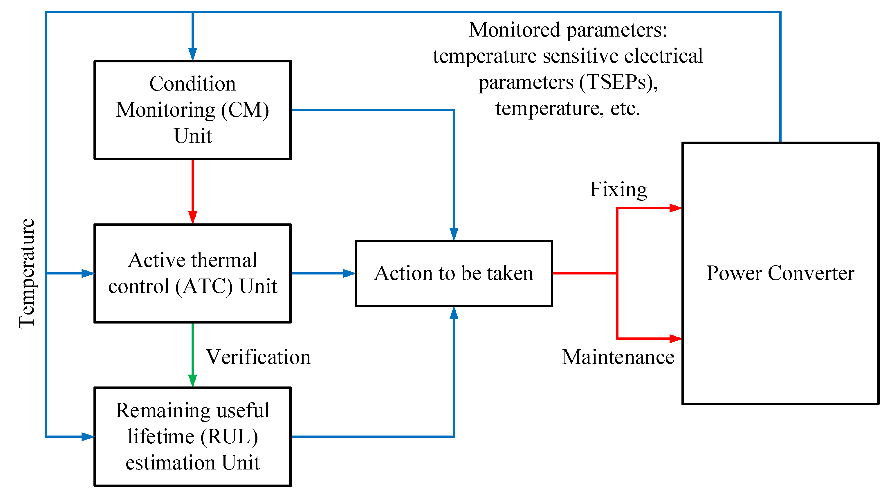
2. Condition Monitoring Techniques

Because of the relatively large number of publications dealing with CM, this report is therefore not exhaustive. This study attempts to focus on recent techniques proposed since the review performed by Yang et al. in 2010 [12], and the study simultaneously is more concentrated on online CM methods, which can be employed in real-time operation of the power converters. The CM definition can be explained that the technique targets tracking variations in the electrical parameters that are an indication of device degradation or incipient fault [20]. Because monitoring all of the electrical parameters is not practicable in a power converter, specific parameters should be recognized depending on the dominant aging failure mechanism. In addition to the silicon (Si)-based semiconductor device such as the IGBT based power converter, SiC semiconductor devices have been developed and commercialized recently due to their superior properties compared to Si counterparts, like the ability to operate at higher temperatures, increased blocking voltages, faster-switching speeds, and higher thermal conductivity [21,22,23,24]. However, compared to IGBT, degradation monitoring methods for SiC devices have not been reported as extensively in literature due to the relative nascence of SiC device technology. Therefore, in this study, the failure mechanism and the CM techniques for IGBT and SiC MOSFET will be reviewed together.

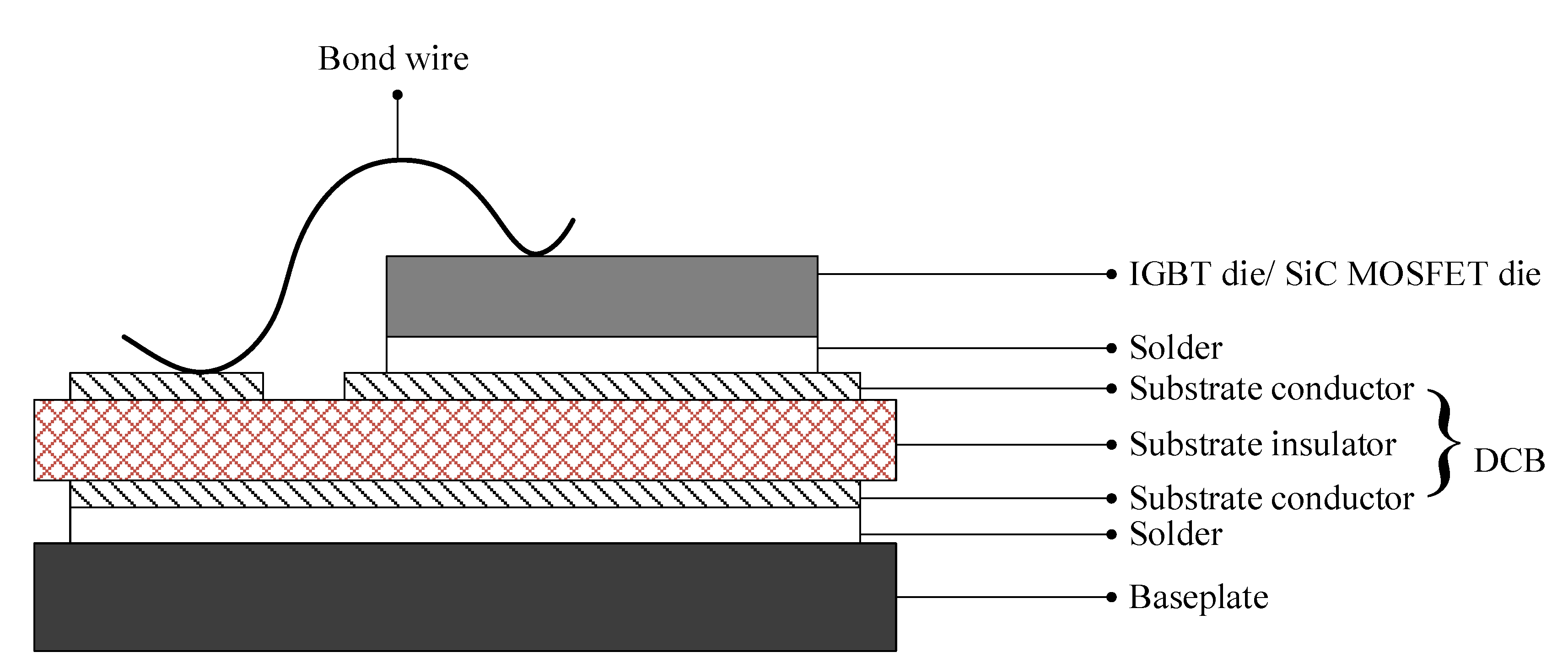
2.1. Failure Mechanism and Indicators
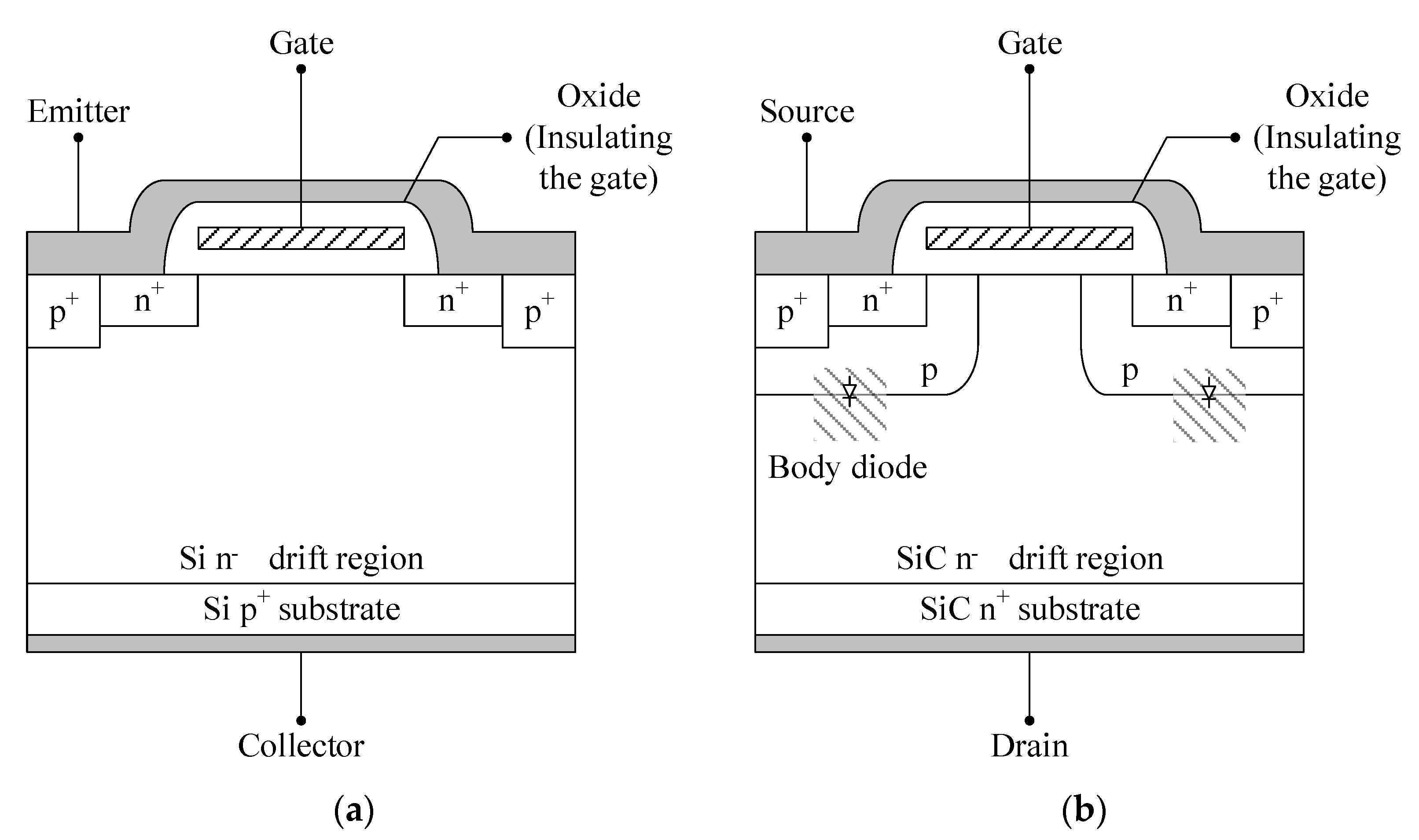
IGBT and SiC MOSFET have a similar chip-level structure, except for an additional p+ layer above the collector in IGBT and an additional body diode part in SiC MOSFET and, as seen in Figure 3a,b. The most popular chip-level failure types in IGBT and SiC MOSFET is the gate oxide degradation failure. The gate oxide degradation failure is caused by high temperature and high electric field stress. Compared to IGBT, SiC MOSFETs are more often applied with the higher gate-source voltage V g s and a higher temperature to achieve lower on-state resistance and a smaller heat sink. This would make the gate oxide more vulnerable [25]. The gate oxide degradation failure in IGBT and SiC MOSFET increases the threshold voltage V t h [26,27]; gate leakage current [28,29,30]. Furthermore, since the gate oxide degradation, the gate oxide capacitance increases, resulting in extending the Miller plateau time duration t g p [31,32]. The on-state resistance can be considered as an indicator for the gate oxide degradation failure in SiC MOSFET [32,33,34], but it has been more often than not utilized to identify the package-related failures. In the SiC MOSFET, there exists a body diode formed by the n- drift region and the well of the p-type semiconductor. In addition to the gate oxide degradation, the SiC MOSFET body diode degradation is caused by the forward voltage bias stress [35,36,37] because of the stacking fault mechanism. In this case, the forward current flowing path is blocked by these faults. Thus, both the on-resistance and forward voltage of the body diode would increase [38]. The on-resistance [35], forward voltage [39], and drain leakage current [25] are considered as indicators for the body diode degradation.
Although some new packaging technologies are introduced, especially for power modules to enhance the reliability, still, conventional packaging and wire bonding techniques are utilized for the majority of commercial IGBT and SiC MOSFET. Figure 4 illustrates a typical package-level structure for both IGBT and SiC MOSFET due to them sharing the same package-level structure. A direct copper bonded (DCB) substrate is soldered to a baseplate. The DCB provides electrical insulation between power components and cooling systems. Further, it conducts the current via copper tracks and also provides excellent thermal. The baseplate provides thermal capacity and helps for the thermal spreading by increasing the contact area to a heat-sink. IGBT and diode chips are soldered to DCB. Bond wires are commonly utilized in order to connect the emitter of the Si/SiC chips to the substrate and in order to connect the substrate to the terminals. The chip die and the DCB, as well as the baseplate and the DCB, are commonly attached by solder. It can be observed in Figure 4 that the IGBT and SiC MOSFET modules contain various layers, and each layer has been made of different materials, resulting in a different coefficient of thermal expansion (CTE). The switching devices produce the switching loss and conduction loss, and they produce thermal stress in the power module [40,41,42]. The converter load variation, the periodical commutation of the power switching device, and the ambient temperature change cause the temperature variation in the power semiconductor module. The significant CTE mismatch between the bond wires and chip under the temperature variation causes the thermomechanical stress in bond wires and, finally, leads to bond wire lift-off or crack failure [43,44]. The bond wire failures cause an increase in the resistance of the bond wires. Consequently, the on-state voltage will increase, which can be identified to indicate bond-wire failures (on-state collector-emitter voltage V c e , o n in the IGBT module and on-state drain-source voltage V d s , o n in SiC MOSFET module) [26,45,46,47]. Other indicators of the bond wire failure are listed in Table 1. Another dominant failure mechanism that occurs in IGBT and SiC MOSFET is solder layer fatigue. The two solder layers in the IGBT/SiC MOSFET module, as shown in Figure 4, are the die attach between the Si/SiC die and DCB and substrate attach between DCB and baseplate. The temperature fluctuations and the CTE mismatches between the Si/SiC chip and solder material, DCB, and solder material slowly generate cracks and voids in the solder layer, resulting in solder layer fatigue. The solder layer failure reduces the thermal dissipation capability, which leads to the increased thermal resistance R t h . Thus, the junction temperature of the power devices rises. As for solder layer failure, the junction-to-case thermal resistance (or thermal impedance) is usually utilized as an indicator to indicate the solder fatigue in IGBT and SiC MOSFET [48,49]. Additionally, the solder layer resistance and junction temperature are utilized to indicate the solder layer fatigue in SiC MOSFET [50] and IGBT [51,52], respectively. The typical failure indicators of IGBT and SiC MOSFET are summarized in Table 1.

2.2. CM for IGBT

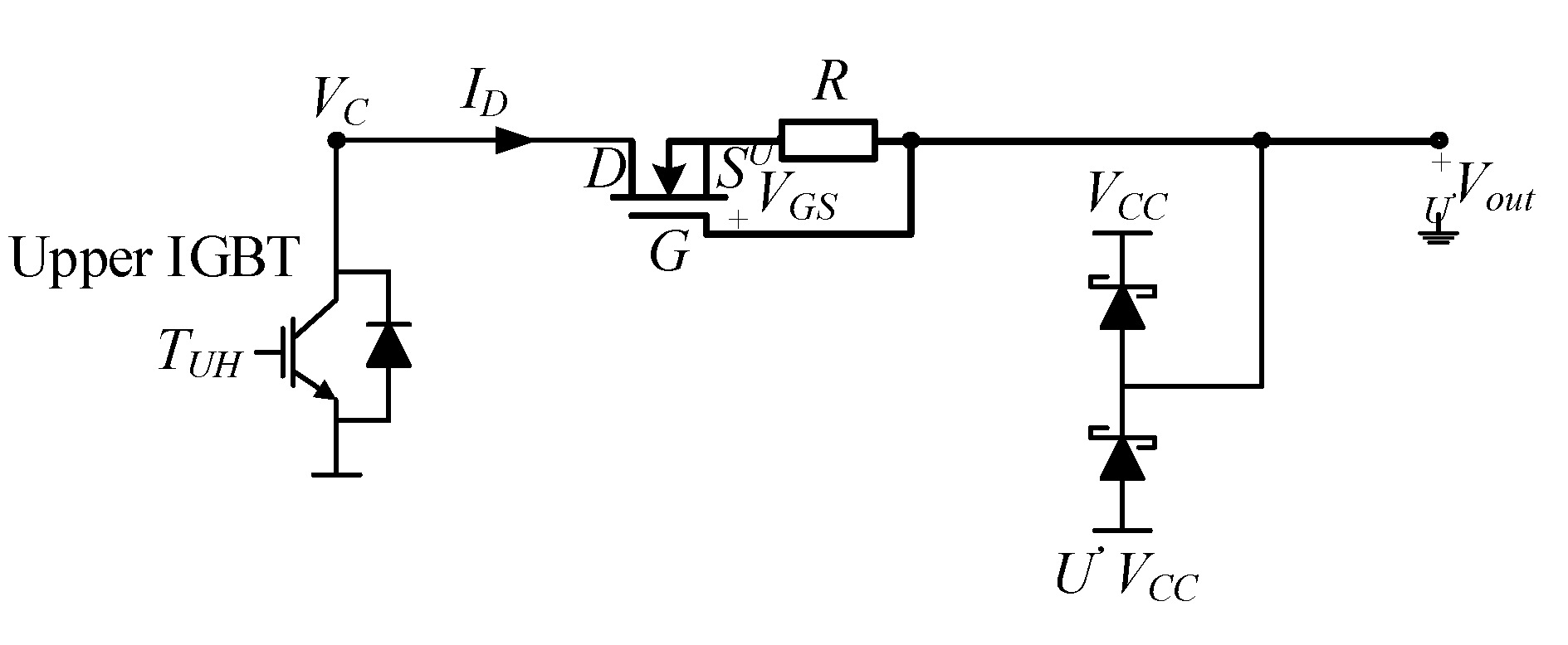
2.2.1. Monitoring Collector-Emitter on-State Voltage

The on-state voltage of an IGBT is a representative electrical parameter indicating the aging failures, and it is the favored indicator for CM technique, which can be recognized by various previous studies on V c e , o n [53,54,55,56]. The increase of on-state voltage is usually utilized as an indicator for wire bonding failure. For instance, the criterion to detect bond wire failure was a +5% [53,54] 15% [55] and 20% [53] increment of V c e , o n from the initial value. From the discussion in [13], the real-time monitoring V c e , o n is challenging because the measured value of V c e , o n can be overwhelmed by signal noise or disturbance during switching. Furthermore, the V c e , o n is influenced by the junction temperature. Therefore, the measurement of V c e , o n should be carefully conducted by evaluating the effect of individual circuit components, corresponding failure mechanism, and junction temperature.
One of the first online V c e , o n measurements was proposed in [57], using two diodes derived from a typical desaturation protection circuit. This approach can measure V c e , o n under the converter operation, but the deviation between the two diodes could lead to the measurement error. Therefore, this technique requires strict requirements regarding that two diodes as the similar currents flowing through, the similar junction temperature level, and forward voltage temperature coefficients. A diode with low reverse recovery and high blocking voltage should be used to ensure accurate measurement. In order to resolve the previous problem of CM using V c e , o n , the author in [58] proposed an intelligent on-state collector-emitter voltage measurement circuit and CM strategies depending on converter operation conditions. The proposed real-time measurement circuit of V c e , o n is shown in Figure 5. For instance, in order to measure the V c e , o n of the upper IGBT, the drain of n-channel small-signal MOSFET in the measurement circuit is connected with the collector of the upper IGBT ( T U H ). The measurement of V c e , o n is conducted during a positive I D current period as a positive value. The measurement of V c e , o n for the lower IGBT also can be implemented in the same manner. The proposed online V c e , o n measurement approach was conducted for both converter application with the fixed operating condition and varied operating condition, considering the temperature dependence of V c e , o n , which confirmed the feasibility and effectiveness of the proposed method.
Another real-time on-state voltage calculation based on the control variables and junction temperature for modular multilevel converter (MMC) submodule (SM) IGBT was proposed in [59]. The on-state voltage of IGBT SMs in MMCs is calculated from the on-state resistance as follow:
V c e , o n = R c e × I c + V c e 0 .
The correlation between the on-state resistance and the junction temperature for a new IGBT is usually given in the datasheet. For the certain aging state as a solder layer, the on-state resistance at a particular junction temperature can be described as following:
R c e , T = R c e , 125 + ( T j 125 ) × k c e ,
where R c e , T is the on-state resistance at a specific junction temperature, T j is the junction temperature, and k c e is the slope value of R c e T j characteristic curve. A function sets of the on-state resistance are deduced by applying the Kirchhoff voltage laws (KVL) in one MMC arm for positive and negative current directions independently. Consequently, the on-state voltage is calculated following the matrix format of the on-state resistance. The proposed measurement method is implemented repeatedly, and the results are continuously calculated every sampling instant. Hence, the Kalman filter is utilized to enhance the calculation accuracy. This proposed technique does not require the external circuit as the method in [59] but needs a relatively high calculation effort in the controller. Additionally, the accuracy of results in this method strongly depends on the measurement accuracy of junction temperature, capacitor voltages, arm voltages, and arm currents. Compared with previous approaches, this method can reduce the costs and avoid the modification of the system. However, it also requires to build a more complex model of the IGBT considering the coupling relation to ensure the accuracy of measurements.

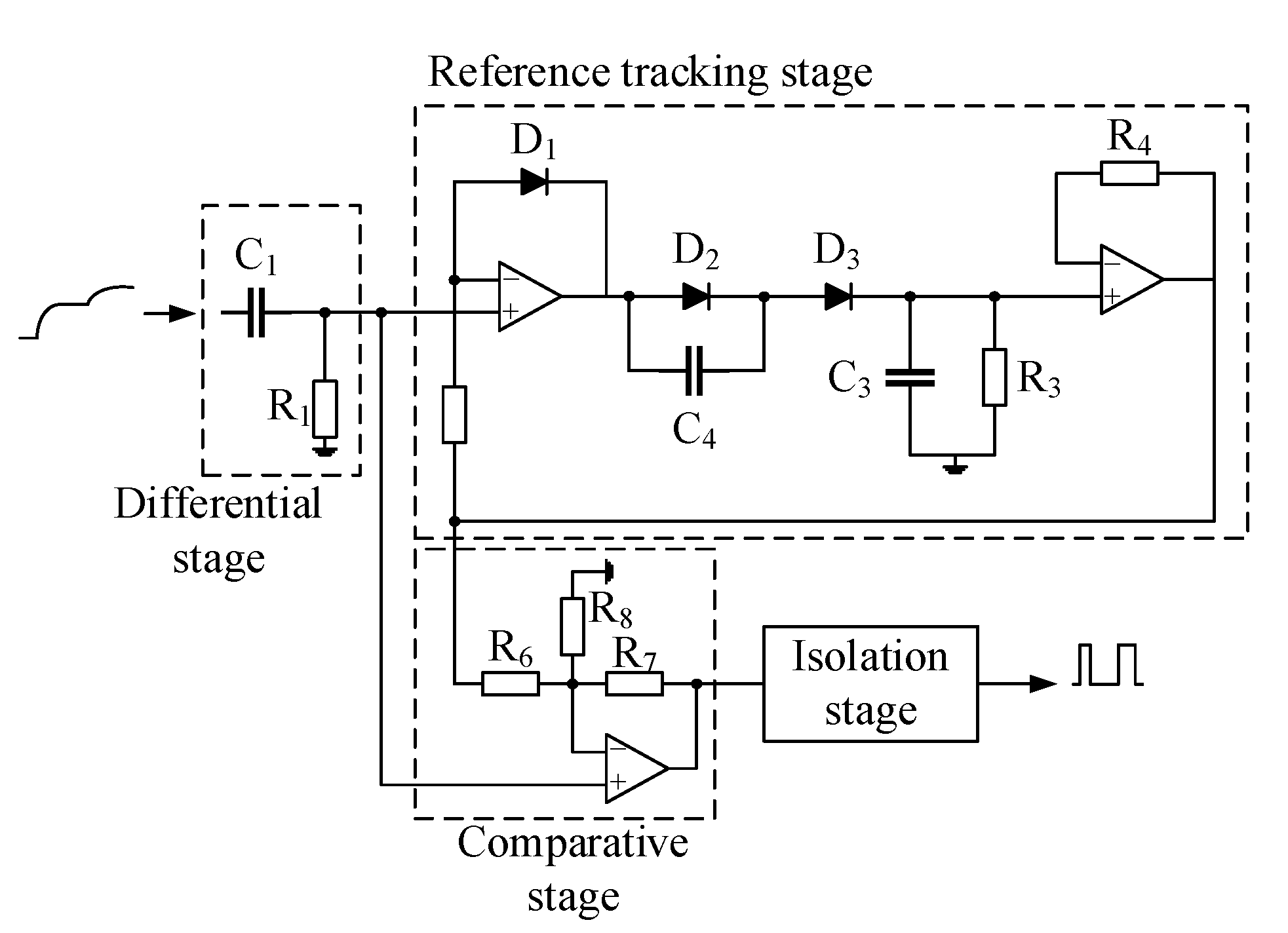
2.2.2. Monitoring Miller Plateau Time Duration

In [60], an in situ CM technique for IGBTs based on the Miller plateau duration during the turn-on transition was proposed. As illustrated in Figure 6, the configuration of the Miller plateau duration detection circuit includes four main parts: the differentiator stage, the comparator stage, the reference voltage setting stage, and the isolation stage [60]. The gate voltage signal is received and differentiated by using a simple RC network. A fixed reference voltage, which represents the rising rate threshold of the gate voltage signal, can be utilized for comparison. Besides, an adjustable reference voltage that depends on the differentiator output can be generated by using a voltage reference generating circuit and voltage divider R 6 , R 7 , R 8 to implement the measurement under different operating conditions. The comparison between the differentiator output and the adjustable reference voltage is employed to produce the double-pulse signal, which deduces the information of Miller plateau duration. The isolation stage is utilized to isolate the analog circuit and the digital circuit. The main design requirements of the proposed measurement circuit can be listed as the time constant should be less than 1/10 the width of the input signal, the differential capacitance must be smaller than the input capacitance of the devices under tests (DUT), and the load resistance must be small enough to achieve high bandwidth. Although this method can be used without interrupting system operation, it requires an accurate calibration procedure to avoid the effect of the changing operation points. Moreover, the practical implementation of this method is preferred for the IGBT in a low-switching-speed application where the measurement uncertainty is reduced.

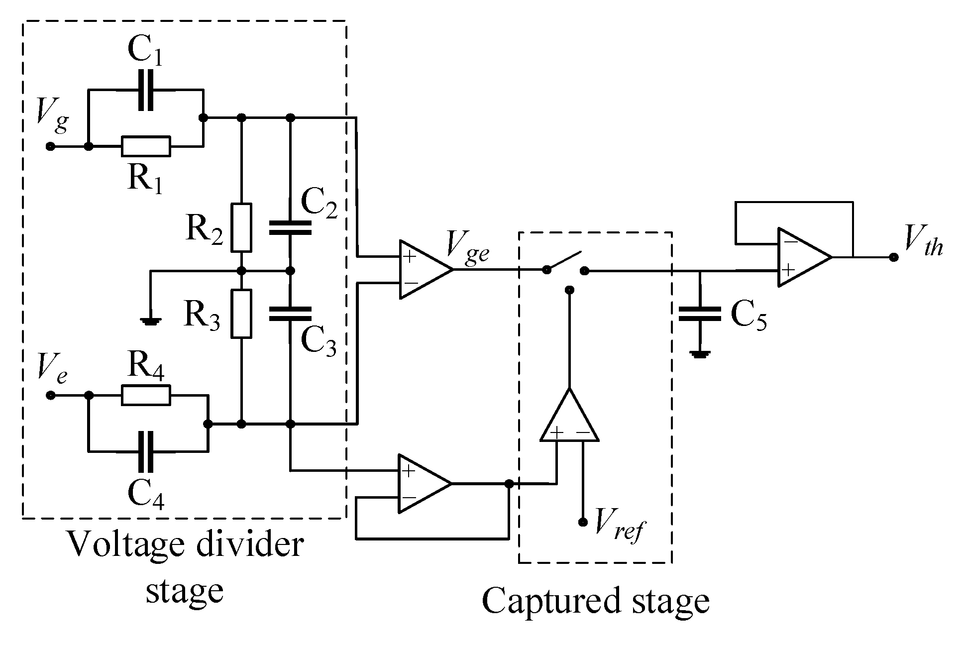
2.2.3. Monitoring Threshold Voltage

The threshold voltage is the minimum gate-emitter voltage V g e required to form an inversion layer at the interface between the substrate region and the gate oxide at the MOS-structure in the IGBT. This inversion layer constitutes a conducting channel that allows the collector current to pass from collector to emitter. It can be described as:
V t h = V F B + 2 Ψ B + 4 ε S q N A Ψ B C O X ,
where V F B is the flat-band voltage, q is the elementary charge of the electron, ε S is the silicon dielectric constant, N A is the doping concentration, C O X is the capacitance of the oxide, and Ψ B is the bulk potential. An increase in V g e , t h was identified in thermal over-stress tests of IGBT components. The increase in V g e , t h is considered as an indicator for gate oxide degradation [26]. Previous studies have to interrupt IGBT’s operation to employ the measurements of V g e , t h . In order to overcome this problem, an online measurement method for V g e , t h was proposed in [61] by using an external circuit, as shown in Figure 7. The V g e is obtained from a voltage divider stage and an amplifier. The voltage drop across the parasitic emitter inductance is compared with a reference voltage V r e f to capture the voltage value at the instant of current initiation. The captured value is utilized to estimate the threshold voltage. It should be noted that the variation of V g e , t h is affected by temperature, so the effect of junction temperature should be combined during the V g e , t h measurement.

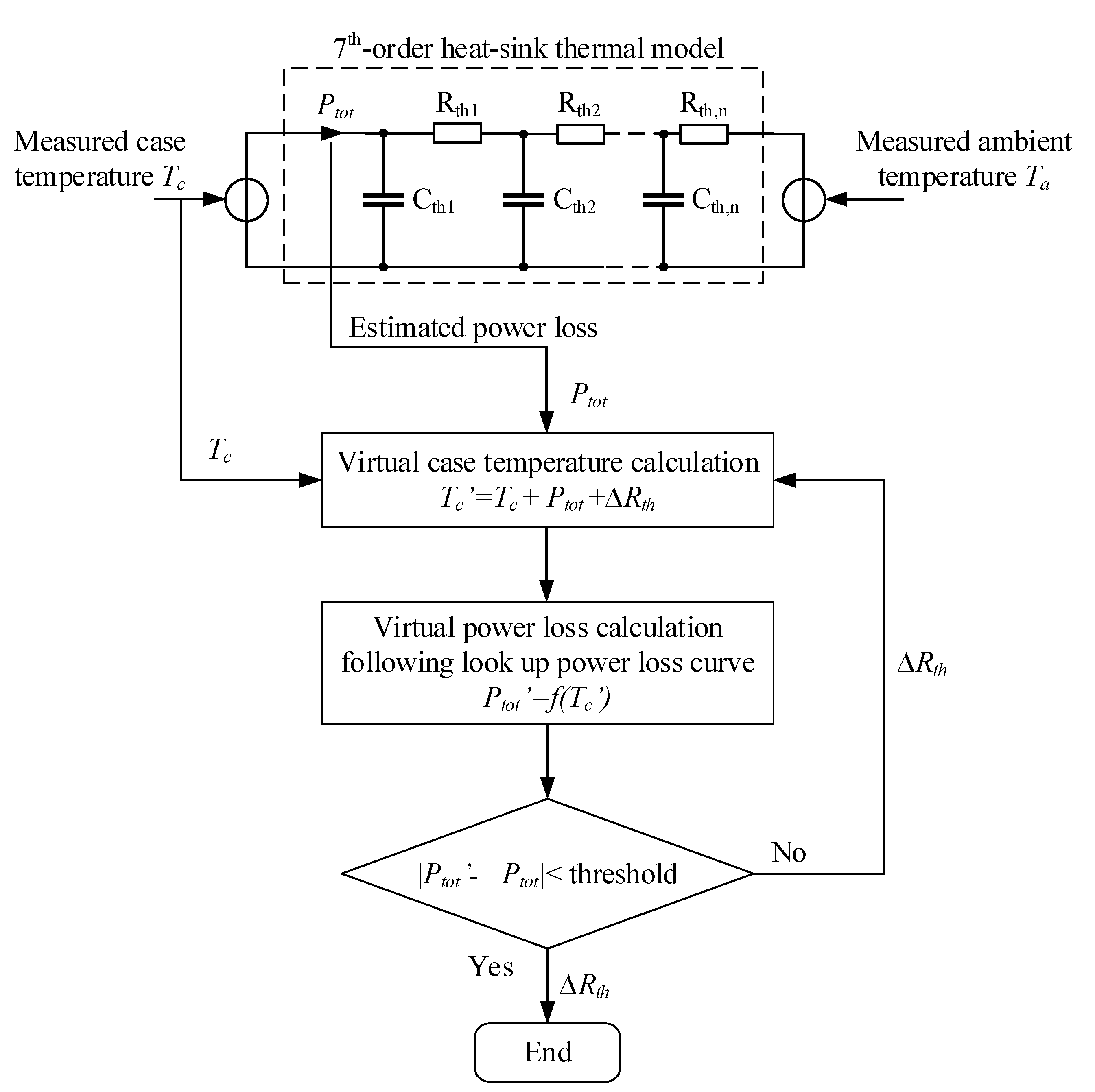
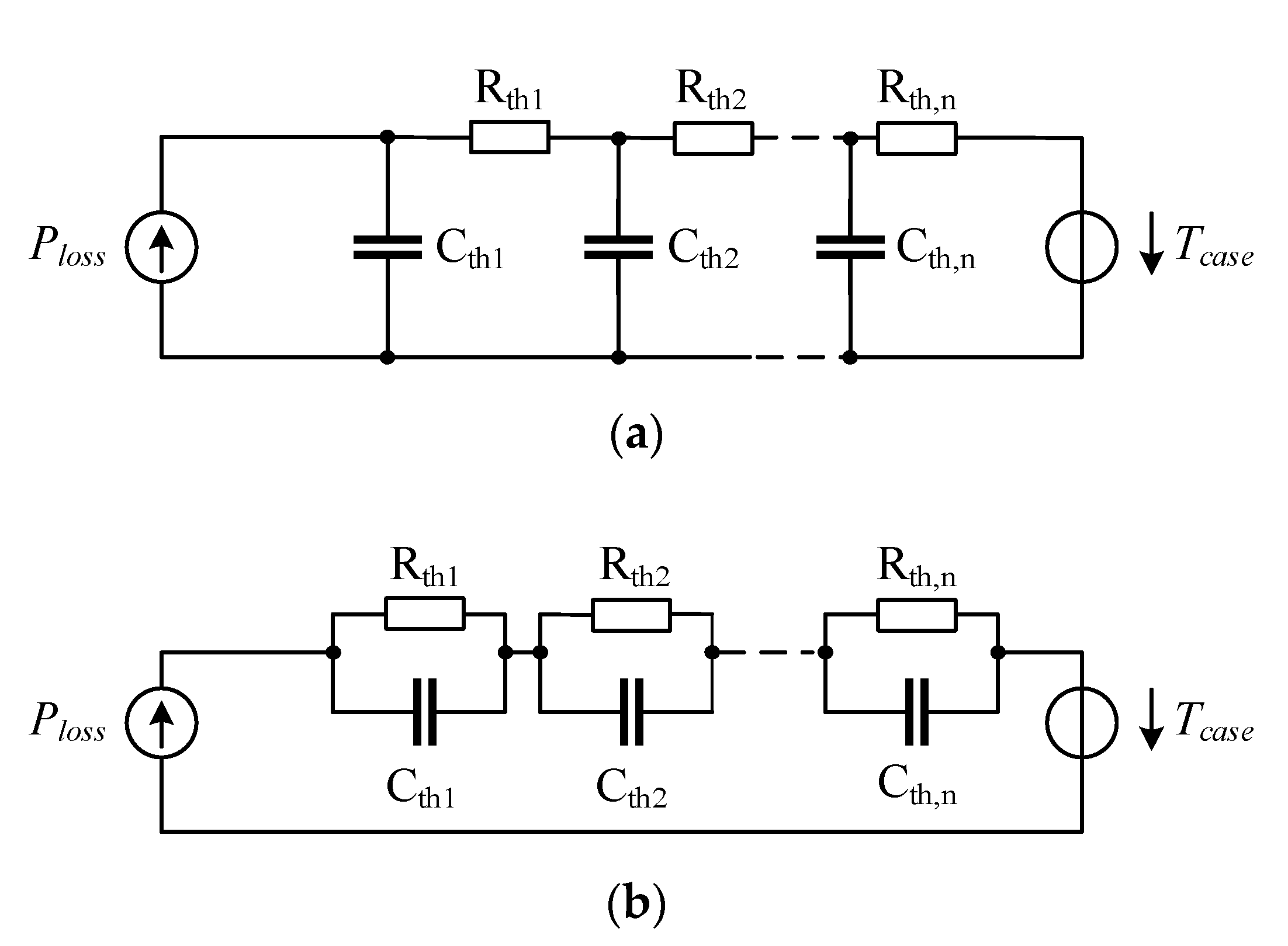
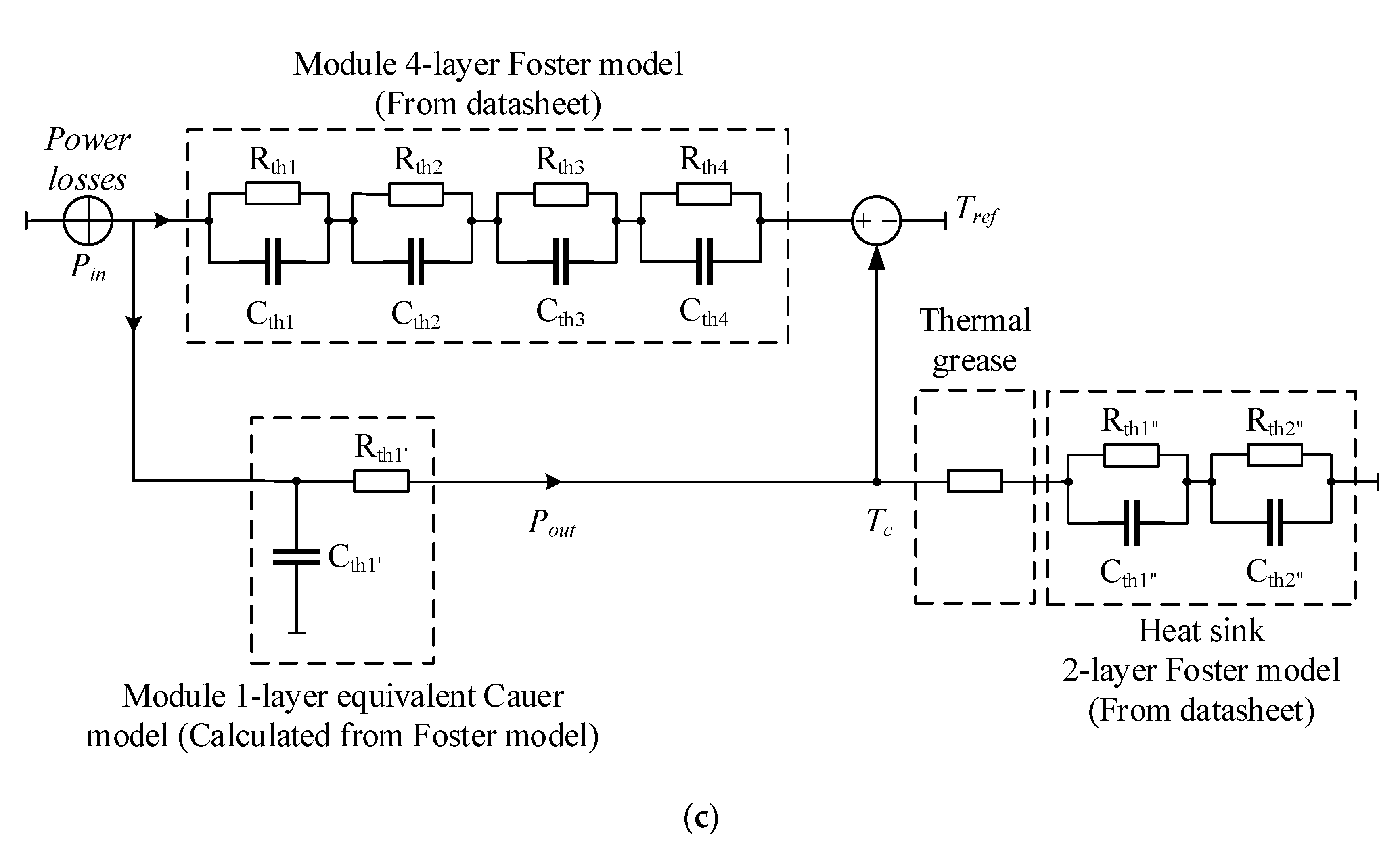
2.2.4. Monitoring Junction Temperature and Thermal Resistance

The junction temperature during converter operation can be utilized as an indicator for the CM technique [44,45]; however, it is difficult to measure directly. Without using an integrated sensor in the device to avoid modifying the package or housing, the junction temperature in CM methods is indirectly calculated by using the temperature-sensitive electrical parameters (TSEPs). The TSEPs can be divided into two main types: static parameter based technique and dynamic parameter based technique, as shown in Table 2. The various techniques, which use different TSEPs, are discussed below.
  • Calculate the junction temperature using the on-state collector-emitter voltage at a high current.
In [62], the relation between the V c e , h i g h and a given current level is generated as a function to estimate the junction temperature from a preliminary I-V characterization curve. From this relation, the junction temperature can be estimated from the measured current and the V c e , o n as follows:
T j _ e s t = S F ( I ) × ( V c e , m e a s u r e d V c e , B ( I ) ) + T B ,
where S F ( I ) is the slope factor as a function of the current, V c e , m e a s u r e d is the measured on-state V c e in real-time, V c e , B ( I ) is the base on-state V c e as a function of current which can be chosen among the characterization curves, and T B is the base temperature corresponding to base on-state V c e . Due to the effect of interconnection resistance, which leads to lower V c e , h i g h measurement. Subsequently, the estimated junction temperature by the V c e , h i g h at high current is smaller than the real measured result. Compensation is needed to acquire accurate junction temperature estimation. The internal resistance variation can be described as (5), whereas the on-state voltage compensation can be expressed as (6):
R i n t = α × ( T j _ e s t T H ) × R V F ,
V c e , c o m p = α × ( T j _ e s t T H ) × R V F × I ,
where T H is the heat sink temperature, α is the scaling factor, RVF is the resistance variation factor, and I is the output current. Hence, the junction temperature after compensated can be calculated as:
T j _ e s t _ c o m p = S F ( I ) × ( V c e , m e a s u r e d V c e , B ( I ) + V c e , c o m p ) + T B .
  • Calculate the junction temperature using the on-state collector-emitter voltage at a low current.
Different from the calculation of the junction temperature using the on-state collector-emitter voltage at high current, the temperature coefficient for the low current is negative [62]. This method is preferred due to its simplicity and adequate sensitivity which is about −2 to −2.5 mV/°C for few hundreds of mA sensed current [63]. Such a low current does not produce any noticeable extra heating at the device, and it can be applied continuously when the IGBT is in on-state.
  • Calculate the junction temperature using the gate internal resistance.
The previous junction temperature using gate internal resistance R g , i n t studies have been reported in [64,65]. Although these approaches have a good result, they require modifying the substrate layout to facilitate the measurement. The proposed method in [66] considers the equivalent series resistance of both gate emitter capacitor and gate collector capacitor as R g , i n t to form the gate driver RLC without disrupting the converter operation, as shown in Figure 8. During the turn-on delay, both C g e and C g c are constant before the gate voltage equals the threshold voltage V t h . The gate current I g can be utilized as a step response of the RLC network, and the parasitic gate inductor should satisfy R 2   >   4 L / C . Subsequently, the RLC network is overdamped, and the gate current I g can be approximated.
I g = V R e t R C
Using a peak detector circuit, as shown in Figure 8, it can monitor the peak gate current by measuring the peak value of the voltage across the external gate resistor. Hence, the internal gate resistance can be calculated as:
R g , i n t = V g , p o s V g , n e g V p e a k d e t e c t o r / R g , e x t R g , e x t .
Subsequently, based on the calibration, the junction temperature can be estimated. The result in [66] showed a strong linear relationship between the resistance and the estimated temperature. However, due to the assumption during measurement and calibration, there might be measurement errors.
  • Calculate the junction temperature using short-circuit current.
In [67], the authors proposed a method using short-circuit current-based estimation to calculate the junction temperature in using an additional bypass switch as shown in Figure 9. The relation between the short-circuit current and the temperature is a negative coefficient [68,69,70]. The bypass IGBT is connected in parallel with the complementary IGBT and is active only when the switch under test is in the off state to create short-circuit conditions. The short circuit current amplitude is approximately linear, with the junction temperature with an adequate temperature sensitivity of 0.35 A/°C. Although the duration of short-circuit time is short, the repetitive short circuit could have a cumulative degradation effect on the device, which should be taken into consideration if the short circuit current is adopted for online temperature measurement.
  • Calculate the junction temperature using the threshold voltage.
As stated before, the threshold voltage is the gate emitter voltage when the device begins to turn-on. In [71,72], a SEMIKRON SKM-75GB12T4 IGBT was utilized as an experimental IGBT to obtain the junction temperature estimation model based on V g e and t d o n . By conducting an offline calibration experiment under different temperatures and bus voltages, the negative relation between V g e and temperature and the positive relation between V g e and bus voltage are deduced. Consequently, a model, which presents the exact correlation between t d o n , T j , and V g e can be described as follows:
T j = 1.24 V g e + 132.84 t d o n 23969.7 .
The obtained model can help measure the junction temperature without interrupting the regular operation of IGBT. Besides, this model rejects the effect of the bus voltage and only requires measurement of the voltage signal, V g e . Hence, the measurement circuit is easy to implement, and it is not hard to confirm accuracy.
  • Calculate the junction temperature using Miller plateau voltage.
Following [73], the Miller plateau voltage can be calculated according to (11) using the threshold voltage V t h and transconductance gain K n , both of which can be influenced by the junction temperature:
V g p = I c e K n + V t h .
However, the junction temperature cannot be directly estimated based on the Miller plateau voltage calculated in (11). Due to the internal gate resistance, which is placed inside the power semiconductor, the gate voltage is unreachable. In order to overcome this problem, the measurable Miller plateau voltage can be utilized to estimate the junction temperature. The measurable Miller plateau voltage can be presented as a function of the Miller plateau voltage, the gate driver voltage, and the internal and external gate resistance:
V m , g p = V g p + V ,
V = ( V d V g p ) × R g , i n t R g , i n t + R g , e x t .
Consequently, the junction temperature can be estimated by using a lookup table based on the measurable Miller plateau voltage and the device current I c e .
  • Calculate the junction temperature using turn on/off delay time.
As stated in [71], the dynamic TSEPs can be influenced by the bus voltage or load current. The turn-on delay time is calculated as the time between the rising edge of the gate-emitter voltage and the rising edge of the collector current, or the time within the gate voltage reaching the threshold voltage [74]. The turn-on delay time was defined which is suitable to be utilized as TSEP. The results showed that the turn-on delay time has excellent linearity with the temperature. However, due to the influence of the bus voltage, the measurement can only be conducted when the bus voltage is kept constant. In order to overcome this problem, the author in [75] proposed a method, which utilized both turn-on delay time and the maximum increasing rate of collector current to calculate the junction temperature, eliminated the effect of the bus voltage. The relations between the junction temperature and the turn-on delay time can be described as:
T j = 1 | a 11 a 22 a 12 a 21 | × [ ( a 22 × t d o n a 12 × V e E _ m a x ) + ( a 22 × b 1 + a 12 × b 2 ) ] ,
where a and b are the constant coefficients after the calibration process and V e E _ m a x is the maximum voltage that crosses the parasitic inductor L e E .
In addition to the turn-on delay time, the turn-off delay time, which is defined from the time point when the gate-emitter voltage falls to 90% maximum value to the time point when the collector-emitter voltage rises to 90% off-state value. In [76], a simple measurement circuit including current/voltage collecting part, voltage reference part, voltage divider, signal processing part, isolation circuit, and DSP controller, was proposed to estimate the junction temperature based on the turn-off delay time as shown in Figure 10.
Following the definition, the turn-off delay time can be calculated following as:
t d o f f = t 1 + t 2 ,
t 1 = R G ( C g e + C g c ) l n ( 0.9 V g e ( o n ) V g e ( o f f ) V g p V g e ( o f f ) ) ,
t 2 = R G C g c 0.9 V d c V c e ( o n ) V g p V g e ( o f f ) .
It can be observed that the turn-off delay time increases with increased V d c as the turn-on delay time.
According to the discussions above, it can be noticed that resolving junction temperature from the measurement of TSEPs can be challenging due to many reasons as the low sensitivity of junction temperature, dependence on loading conditions, and measurement inaccuracies. The ideal TSEPs can be applicable to any device type, any converter topology, suitable for any application. However, for the case of online TSEPs measurements, the proposed solutions may only be adaptable to particular converter topologies. Therefore, some TSEPs have advantageous qualities, but due to implementation issues, they may only be able to be sampled periodically without causing unacceptable disruption to normal converter operation.
  • Monitoring thermal resistance.
The increase of the internal thermal resistance R t h by 20% of the nominal value in [35,77] can be adopted to indicate the solder fatigue. The thermal resistance increase usually is approximately equal to:
R t h T C P t o t ,
where T C is the temperature change due to the increase in power loss. The detailed principle of the method in [78] is shown in Figure 11. The power loss was first estimated from a thermal model that utilized temperature measurements as inputs. A lookup table that provided the information of power loss in healthy IGBT modules was subsequently incorporated, which enabled the estimation of solder layer damage under various operating conditions. It should be noted that due to the correlation between junction temperature, case temperature, and power loss, the measurement should be employed correctly. The implementation of the method requires consistent measurements and online calculation, which can be carried out by the controller digital signal processor, and an iterative calculation is recommended to provide a running update of the changes in thermal resistance.

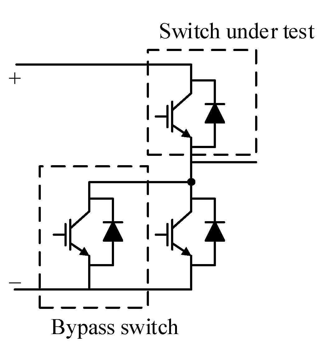
2.2.5. Other Monitoring Techniques

  • Embedded sensor-based CM techniques.
The first embedded sensor-based CM technique was first developed in 2003 to detect bond wire lift-off in an operating power module [79]. Redundant bond wires are attached to the emitter of the die. Bond wire failure was detected when the resistance between the emitter terminal and the sensor terminal deviated from a nominal value. Although it provided accurate detection of bond wire failure regardless of the operation, the technique required a modification of the original design of IGBT modules and implementation of the monitoring circuit in a gate driver.
Recently, a work proposed a technique for using the already integrated current sensors in the IGBT power module for monitoring of the bond wire lift-off failure [80]. That integrated current sensors are giant magnetoresistive (GMR) detectors, which are utilized for current and ambient temperature sensing [81,82]. The basic idea is that these detectors are placed near the bond wires, and the change in the magnetic field caused by any lifted bond wires will be sensed. In [80], two GMRs are required to sense the current, where GMR1 senses the low-frequency current, and GMR2 extends the current sensing bandwidth. In the case of bond wire lift-off exists, the flux density sensed by one GMR will be less because the lifted bond wires no longer carry current. The remaining GMR will have a slightly higher flux density because the current is forced to flow through the remaining bond wires. Although the utilization of GMR does not require modification of the IGBT module, the proposed method requires accurately extracting the lift-off monitoring signals. The proposed method in [83] also does not require any modification to the DCB layer compared with the technique in [79]. Besides, this approach can identify the number of lifted bond wires and locate these lifted wires. The Kelvin connection is realized by introducing additional terminals. The emitter side of the IGBT chip is connected with the added Kelvin pins. When bond wire lift-off occurs at a specific chip, the corresponding on-state voltage V c K e will decrease, whereas the remaining V c K e increases.
  • Converter output-based techniques.
The converter output-based CM technique identifies variations in the voltage and current output of power converters. Although this approach does not need any additional sensors and modification in switching devices, the converter output-based CM technique has to operate at a specific condition, which makes it is hard to identify the harmonic amplitude in real-time operation. Besides, the identification of specific aged devices requires additional tools. Therefore, the utilization of the converter output-base technique for CM is limited. A well-known study was reported by Xiang measuring the fifth harmonic of the output current to monitor the solder fatigue [84]. The small change of fifth harmonic current with respect to a specific case temperature for a given load level is measured by the converter controller. Further study is required to improve the converter output-based CM technique to increase the number of aging indicators from converter output, conducting the approach in real-time operation, and widely applicable to various converter types.

2.3. CM for SiC MOSFET Module

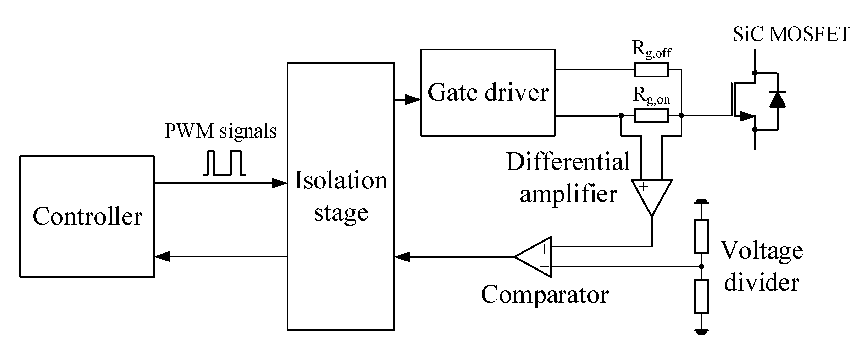
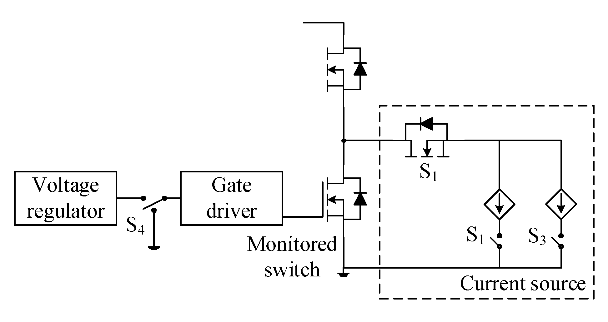
2.3.1. Monitoring Gate Leakage Current

The previous studies defined the gate leakage current i l k as an indicator of gate oxide degradation [85]. The gate leakage current measurement does not utilize any signal from high-current or high-voltage parts of the power stage for monitoring the device. Besides, it has very distinct values for a healthy and aged state. In [86], the author proposed a method for the online aging detection method using the gate leakage current. The block diagram of the proposed method in [86] is illustrated in Figure 12. The gate leakage current is measured by using the gate resistance. A difference amplifier senses the voltage drop on the gate turn-on resistance, then compares the sensed amplified differential voltage to a limit voltage. The limit voltage is utilized as a threshold to indicate the aging effect. From the aging test, it can be realized that there is no leakage current in healthy devices or before the aging effect becomes remarkable. Since there is no current, the comparator logic output will be 0, indicating that the switch is healthy. On the other hand, the gate current will be leaked in the range of a few mA from the aged switch. Subsequently, the logic output from the comparator will be one if the sensed voltage drop exceeds the limit value. This result warns that gate oxide degradation failure might occur in the near future. It is noted that due to the relatively small value of the gate leakage current and the high switching frequency of switch, some requirements for the amplifier, limit voltage is required [86]. Additionally, this method can be integrated into a gate driver chip as an extra protection layer or implemented separately on the power stage to prevent unexpected shutdown depending on the demand.

2.3.2. Monitoring on-State Resistance

The on-state resistance can be utilized as the indicator for both gate oxide degradation and bond wire failures [32,87]. In [88], the drain-source on-state resistance R d s , o n is calculated by utilizing high-frequency network reflectometry. A block diagram of the spread spectrum time domain reflectometry (SSTDR) mechanism [88] is shown in Figure 13, the fundamental of SSTRD is explained in [89]. Since the SSTDR hardware is able to detect any impedance mismatch on its path propagation, it can detect the drain-source on-state resistance due to degradation. By applying high-frequency gate signals to an entirely conducting SiC MOSFET switch, the magnitude of the bounced back voltage is utilized to measure the device impedance variation, drain-source on-state resistance, in this case, over aging. However, this method is not specifically suited to on-board implementation.
In order to resolve the above problem, the author in [90] proposed a practical on-board SiC MOSFET CM technique for aging failures indication, whereas the saturation region on-state resistance R d s , s a t is employed to indicate the die-related aging failure and the drain-source on-state resistance R d s , o n is utilized as an indicator for the detection of package-related degradation. First, the effectiveness of R d s , s a t and R d s , o n as indicators for aging failures are discussed and verified through characterization of a batch of SiC devices aged under accelerated tests. Then, an in situ measurements of R d s , s a t and R d s , o n using readily available system sensors at system startup was proposed, as shown in Figure 14 [90]. As for R d s , s a t measurement, on a switch of a phase leg, is turned on at a reduced gate voltage such that it operates in a saturation region, whereas the other switch in the leg is turned on at full gate voltage (Figure 15a). The measured results from the system current sensor and bus voltage sensor are utilized to calculate the R d s , s a t amplitude of the device operating in saturation mode. Meanwhile, the R d s , o n of the switch is calculated by sensing the V d s , o n across the switch under test and dividing it by the current value obtained from the system current sensor. The magnitude of the V g s for R d s , s a t measurement and R d s , o n measurement are shown in Figure 15a,b. Due to the combination of R d s , s a t and R d s , o n measurement during startup and the use of available current and voltage sensors in the system, this method just requires a simple voltage measurement circuit and reduces the cost of implementation.
In [91], a drain-source on-state resistance is determined by using an integrated module. The voltage between the drain and source V d s and the drain current I d of the switch under test are measured to determine the drain-source on-state resistance R d s . In order to overcome the requirement of certain minimum on-state times during drain-source on-state voltage monitoring, the authors utilized a discontinuous modulation during a fundamental period of the modulation signal to implement for monitoring. The utilization of discontinuous modulation allows measuring the drain-source on-state resistance during normal operation of the converter without interruption for the CM process. Furthermore, the yielded R d s result is stable, and measurement accuracy is not compromised. However, the general output performance of the converter might be affected due to the discontinuous modulation. Therefore, the trade-off should be considered carefully before implementation.

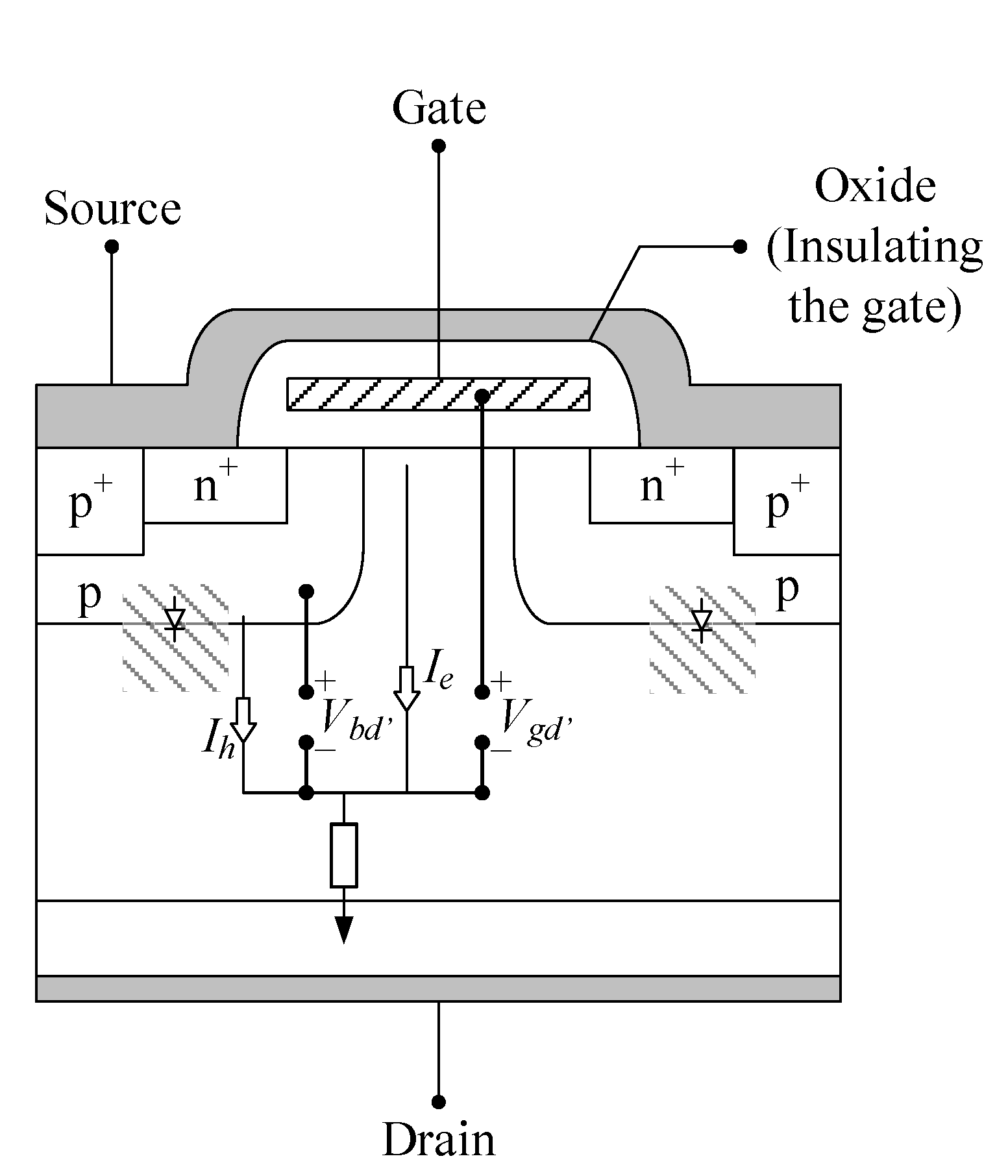
2.3.3. Monitoring Reverse Body Diode

In addition to common aging failure indicators as on-state resistance, threshold voltage, and leakage current, the study in [92] proposed a complete CM method for SiC MOSFETs by using the reverse body diode voltage drop at different gate bias levels. The proposed approach can indicate both the gate oxide and packaging degradations by monitoring a single indicator. In this study, the secondary conduction mode in the third quadrant operation is utilized to monitor the package-related degradation and gate oxide degradation. When a gate bias is between 0 to −4 V, the current flows through the MOS channel, whereas at a negative voltage of −5 V, the current path is through the PiN diode, which does not include the channel as shown in Figure 16 [92]. By combining this analysis and the results from the accelerating aging test, it can be concluded that the body diode voltage drop can detect the gate oxide degradation when the gate bias voltage is 0 V, whereas the package-related degradation can be detected by monitoring the body diode voltage drop at −5 V gate bias voltage. Figure 17 shows the circuit diagram of the gate driver circuit board with a complete CM technique for gate oxide degradation monitoring and package-related degradation monitoring [92]. The switches S 1 S 4 are utilized to toggle the operation mode of SiC MOSFET and the gate bias voltage value to capture the body diode voltage drop. Consequently, gate oxide degradation and package-related degradation are monitored independently. Although the proposed method can utilize a single indicator to monitor two types of degradation, further study is required to conduct the approach during converter operation. Additionally, the complex drive control circuit is a drawback of this proposed approach.
According to the discussion above, the new findings of CM regarding online techniques for both IGBT and SiC MOSFET are presented. The CM techniques are classified following the type of indicators for each type of power semiconductor devices. The benefits and drawbacks of each approach are also given.

3. Active Thermal Control

As depicted in Figure 2, the degradation indicator information obtained from online CM techniques can be applied to not only passively update but also actively control the system lifetime. Therefore, ATC, which is a new idea lately introduced to adjust power losses and thermal stress, is discussed here. The common principle is to vary temperature-related control variables of the power converter to vary the junction temperature, which will reduce damage caused by thermal cycling [16,93]. By using ATC, the reliability of power devices is improved, and the lifetime of the power system is extended. Basically, the control of junction temperature, temperature variation, peak temperature, and average junction temperature has been targeted. From the perspective of converter type, this paper divides the ATC into three main categories: single-converters, cascaded converters, and parallel converters systems. The classification can be described as follows:
(1)
The single converter systems include the two-level, three-level converters in ship power, machine drive applications, and buck/boost converters in the photovoltaic application.
(2)
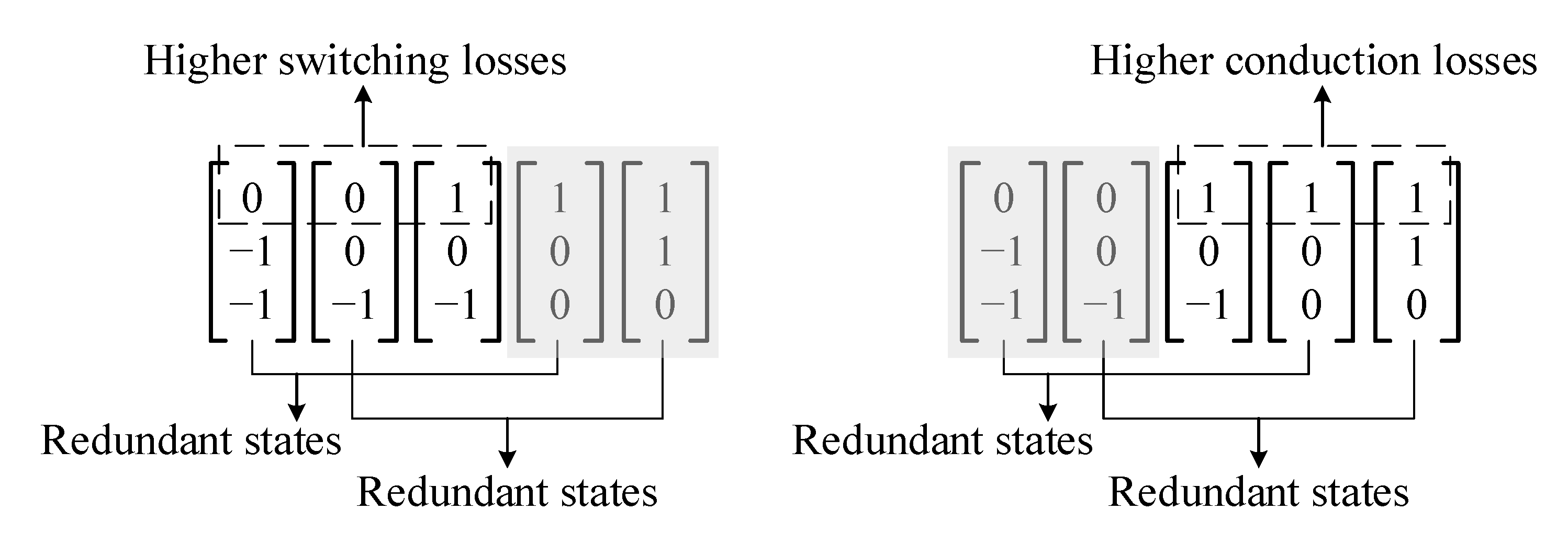
The cascaded converter systems include the cascaded H-bridge (CHB) converters and MMC.
(3)
The parallel converter systems include the systems that utilize parallel structure based on two-, three-level converters, buck/boost converters in wind power, and machine drive applications.

3.1. Single Converter System

A straightforward method to realize thermal control is to regulate the switching frequency, which has a direct impact on the power losses without considerably affecting the working condition of the power system [93,94]. In [95], a switching frequency reduction method based on the junction temperature variation for a two-level inverter in an adjustable speed drive application was proposed. The operating switching frequency is determined through a hysteretic control as follows:
f s = { f s m i n ,   T j * > T 1 f s * ,   T j * < T 2 u n c h a n g e ,   T 1 < T j * < T 2 ,  
where T1 and T2 are the upper and lower limits of the hysteretic junction temperature variations, respectively, adjusting the switching frequency as a function of both the average temperature and the temperature variation together, have better reliability improvement compared with the control of a single parameter. However, the combining of control parameters increases the complexity and calculation burden of the control system.
A different manner is to modify the modulation methods and utilize modern control methods. In [96], a pulse-width modulation (PWM) strategy for redistribution of losses for the three-level neutral-point-clamped (3L-NPC) inverter, named active lifetime extension (ALE), without any additional hardware for the modulation range 0.5 < m < 1 was proposed. There is a total of 27 different arrangements of the switches in the 3L-NPC, as shown in Figure 18. The use of different switching states allows reducing the switching losses or conduction losses. For example, the region, highlighted in blue, presents redundant switching states. If the conduction losses have to be reduced, the switching states yielding higher conduction losses are eliminated from the switching sequence. Conversely, if the reduction of switching losses has the priority, the corresponding states are forbidden, as shown in Figure 19.
The author in [97,98] utilized the redundant switching states in the inner hexagon (region is highlighted in orange) of the space vector diagram to alter the current paths flowing in the power devices and thereby reducing the conduction losses or switching losses of the device. This control scheme is especially suitable for the ride-through operation, during the grid faults for grid-tied converters, or the startup operation of motor drives where the modulation index is low, and the voltage reference is located in the inner hexagon in Figure 18.
The control scheme in Figure 20 shows a junction temperature controller using the finite control set model predictive control (FCS-MPC) to control the amplitude of thermal cycles in a two-level three-phase inverter-based machine drive [99]. The load current, junction temperature, and the resulting thermal stress are predicted for all space vectors of the next sampling instant. These predictions are utilized to derive the FCS-MPC cost function parameters that include the error from the current reference, the thermal stress on the device, the temperature difference between the chips on a power module, and the total power losses from switching and conduction of the semiconductors. These parameters are weighed, and the space vector with the lowest cost function is directly applied to the power converter.
Based on this concept, a sequence of control for a current-source active rectifier was utilized as a control algorithm in [100]. The working principle of the sequence control approach is based on a finite number of switching states of the power converter. To select the optimal switching state, an objective function that computes the error between predicted values and reference values of both electrical and thermal objectives. It can be seen that, by minimizing the multi-objective weighted cost function, the electrical and thermal objectives can be achieved. However, it should be noted that the output performance of the power converter system might deteriorate and the computational burden might be relatively heavy.

3.2. Cascaded Converter System

Modular/cascaded power converters have been gradually utilized in medium- and high-voltage/power applications. The most popular topologies are CHB converters and MMCs. Due to containing many cells/SMs in the power converter system, the unequal thermal stress among cells/SMs exerts a negative impact on the switching devices and the lifetime of the power converter.
The author in [101] proposed a technique, named power routing, to implement ATC through unevenly loading the modules of the modular/cascaded configuration. The power routing method is the optimization technique in which each module processes a quantified amount of power with the aim of improving the system’s efficiency and reliability [101], as depicted in Figure 21. The module can be connected in series or parallel or a combination of both. As for the series connection, the same current is shared among modules, but each module has the degree of freedom to control its output voltage. Thus, the power of the individual module can be regulated by varying the module’s output voltage. Similarly, regarding the parallel configuration, the cells share the same voltage, but each module has the degree of freedom to control its output current, the parameter utilized to control cell power is the current instead of the voltage. Based on this technique, the power routing method is applied to CHB converters [102], 3-stage modular smart transformer comprising a CHB for medium voltage AC (MVAC) to medium voltage DC (MVDC) conversion [103], and dual active bridges (DAB) for MVDC to low voltage DC (LVDC) conversion [104]. Thanks to this method, the most damaged cells can be preserved.
Regarding MMC, this type of multilevel converter has received a great deal of study in terms of various aspects as output performance improvement [105,106,107,108], reduced computational burden [109,110,111], power losses balancing among SMs [104,112,113], etc. Due to the relatively large number of SMs, the ATC is usually conducted to achieve similar thermal stress distribution among the different SMs to enhance the lifetime of the power system [104]. In [114], the unbalanced thermal distribution among SMs, induced by the mismatch in the SM parameters, was analyzed. Due to the SM capacitors are not identical, the switching losses and conduction losses of associated SMs will be different, resulting in unbalanced thermal distribution among SMs. In order to solve that problem, an active thermal balancing control was proposed by combining the junction temperature of lower IGBT and the capacitor voltage to the sorting algorithm by using a weight function. The weight factor is altered between zero and a predefined value to guarantee both the capacitor voltage balance and equal thermal distribution among SMs:
L i = ( 1 α ) × v n o r m i α × T n o r m i × s i g n ( i a r m ) ,
where α is the weighting factor, v n o r m i and T n o r m i are the deviation in the capacitor voltage and the junction temperature, respectively. The acquired experimental results under different cases with different capacitances in SM capacitors validated the proposed thermal balancing control methods by equally distributing the temperature among SMs. However, the capacitor voltages are less balanced, which is a trade-off when the thermal balancing control approach is adopted. Another thermal balancing strategy was presented in [115], integrated the junction temperature to the capacitor voltage balancing algorithm to achieve similar thermal distribution among SMs. Different from [114], the temperature of devices in SM is integrated separately to associated capacitor voltage, forming four cost functions corresponding to the upper IGBT, upper diode, lower IGBT, and lower diode. The cost function is selected for each sampling instant by taking into account the arm current direction and whether SMs have to be inserted or bypassed. The proposed control approach sharply reduced the inhomogeneity and temperature spread among the SMs.
A method proposed in [116] achieved SM thermal balancing by regulating the capacitor voltage of each SM in an arm while keeping the sum of the SM capacitor voltages at nominal value to control the dc-link voltage. As shown in Figure 22, the temperature of each SM T SM , i is compared with the average temperature of all SMs T avg in the arm, and the difference fed to a proportional-integral (PI) controller, which will determine the voltage differential to be added to each individual SM voltage reference [116]. The capacitor voltages are regulated following [117] but with additional terms corresponding to the temperature. Although the temperature among SMs was balanced, a distorted multilevel arm voltage waveform was produced from unbalanced capacitor voltages.
In [118], the study revealed that thermal stress distribution inside the SMs of hybrid MMC (Figure 23) becomes more unbalanced under a high voltage modulation index. The ATC for both half-bridge SMs (HBSMs) and full-bridge SMs (FBSMs) was proposed to solve this problem. As for FBSMs, the two kinds of bypassed switching modes were altered to form a symmetrical switching arrangement when arm voltage is positive [118]; as shown in Figure 24, the same procedure is applied when arm voltage is negative. The symmetrical switching arrangement does not deteriorate the converter output performance, whereas the distribution of power losses in FBSM is more balanced, resulting in the thermal reduction of the most stressed devices.
Meanwhile, a thyristor with high current withstand capacity was connected in parallel with the lower IGBT/diode in Figure 25. The positive arm current will be bypassed by the thyristor to reduce the thermal stress on the lower IGBT. The utilization of a parallel thyristor in HBSM is also applied in the MMC high voltage DC (HVDC) system to protect the lower diode under the DC short-circuit fault.

3.3. Parallel Converter System

The problem of high-current low-output-voltage conversion at the point-of-load is commonly resolved by using a parallel connection of multiple converter units. The parallel converter systems offer a reliability improvement as redundancy quite easily can be implemented. Although the load sharing technique is utilized to distribute the load current and achieve equal sharing of load, it does not guarantee even distribution of thermal stress among parallel converters. The cause of this problem might be the variation in the parameters in the power converters and also the aging effect, which produces the temperature mismatches. In order to overcome this problem, an active thermal sharing was proposed [119,120,121] for a parallel DC-DC converters system. In this method, the load current is redistributed between parallel converters using the temperature values of the power converters. The current and temperature information were mixed together, and the new information is utilized in the average load sharing (Figure 26). This control scheme tends to equalize the thermal stress among the parallel converters. The advantage of this approach is straightforward to implement in the existing system; however, there might be a possibility of a slight increase in the individual converter failure rate.
The system reliability can be improved by using an ATC method-based droop control scheme [122,123]. In [124], a load sharing control scheme among converters was reported. The droop gain will be updated according to the calculated consumed lifetime of the converters. Here, the droop gain was calculated following the accumulated consumed lifetime (ACL) by:
R d , k = A C L k ( p u ) × R d o ,
where R d o is the maximum allowable droop gain. Following the ACL of each converter, the corresponding droop gains need to be adjusted to achieve an equal ACL for all converters. Thus, the load sharing among the converters is achieved based on thermal stress on the semiconductor switches; hence, by actively controlling the loading of converters, the ACL of converters can be equalized, and the overall system reliability can be enhanced.
In addition to the thermal control based load sharing technique, the power routing method is also adopted in the parallel converter system to balance the aging of converter cells. Similar to the power routing principle in the cascaded/modular converter system, the authors in [125,126] utilized power routing in parallel DC-DC converters system and two-level voltage source inverter (2L-VSI) in a triple modular permanent magnet synchronous motor (PMSM) drive system, respectively. The power routing method, based on the aging status of each converter cell in a parallel system, redistributes the power to each converter cell by adjusting the duty cycle to generate the switching patterns in the modulation stage. Consequently, the lifetime of the most aging converter cell is increased to improve the reliability of the whole system.
The parallel converters system for wind power applications in Figure 27 has suffered from a considerable temperature variation due to the wind speed fluctuation. In [127,128,129,130], the ATC is applied in the wind power system by means of reactive power to smooth the temperature fluctuation of power devices during wind speed variation, as shown in Figure 27. In the parallel converter, the reactive power delivered can significantly influence the loading of components, and it is not restrained to the existing mechanical/electrical power processed by the converter system so that it is suitable to achieve ATC. The reactive power will not only adjust the phase angle between the output voltage and current of the converter but also change the current amplitude flowing in the power devices, which are all associated with the power loss and thermal stress of power devices. By introducing a certain amount of underexcited reactive power to heat up the device during the low power period, the overall fluctuation of device temperature can be significantly reduced. The disadvantage of reactive power cycling is that it can only be applied in the parallel converter system, and the thermal load of the diode is increased.

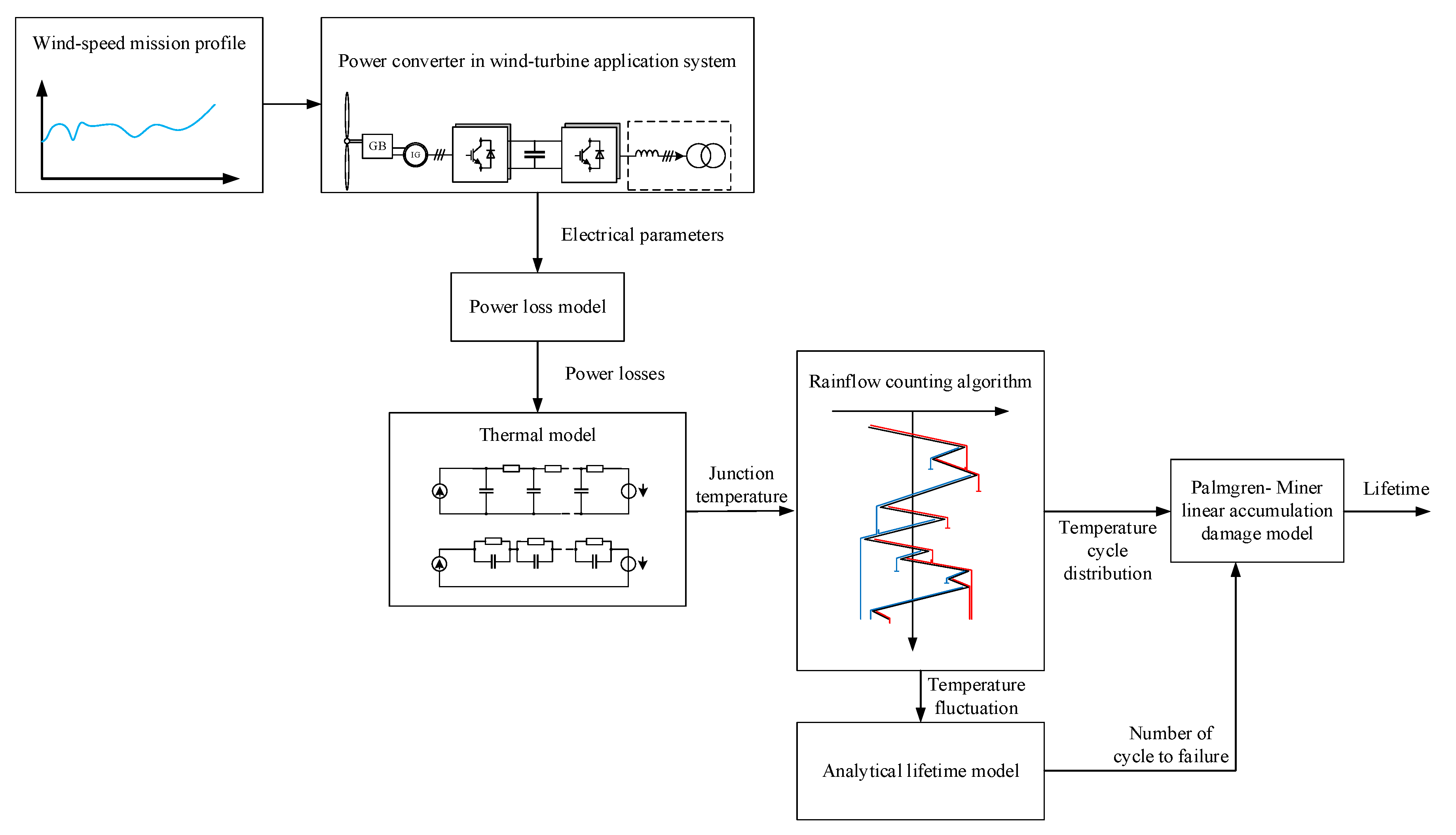
4. Remaining Useful Lifetime Estimation

The RUL of an asset is defined as the length of time from the present time to the end of useful life [131]. The need for RUL estimation is evident because it relates to a frequently asked question in the industry, which is how long a monitored asset can survive based on the available information. Based on the RUL estimation, appropriate actions can be planned. The reported RUL techniques include both model-based and data-driven approaches.

4.1. Model-Based Methods

A typical flow chart of RUL estimation model-based techniques is illustrated in Figure 28. In model-based approaches, typically, junction temperature information is mandatory and utilized in analytical lifetime models such as Coffin–Manson [132] or more detailed Bayerer [133] models, which estimate the number of cycles to failure under given junction temperature swing amplitude. The junction temperature is estimated by computing the power losses and thermal impedance model of the switch following a mission profile of the power converter system. Meanwhile, temperature cycles are counted using the rain-flow counting algorithm [134]. The accumulated damage as a result of different thermal swings is found by using simple linear damage models such as the Palmgren–Miner model [135].
As analyzed in [136,137], correct transforming the mission profile of the converter in the real application as wind power into the corresponding loading profile of the power devices is a challenging task. According to the main causes of loading in a power converter of wind turbine applications, the thermal behavior of power electronic components can be generally classified into three times constant: long term, medium term, and short term. Normally, a 1-year mission profile and hourly mission profile are utilized to estimate the RUL of the power converters. In order to exact the temperature profile from the mission profile, in [138], the electrical parameters are extracted from the mission profile by using the mechanical system, power converter system, and controller. The loss models are used to calculate the losses in the switches and diodes using extracted electrical parameters. The thermal loading or junction temperature can be extracted from the power losses by using the thermal model as Cauer model or Foster model in Figure 29a,b [139]. In [138], the utilized thermal model use mix of both Cauer and Foster thermal models to solve the shortcoming of the two stated models, as shown in Figure 29c. Consequently, the junction temperature of power devices can be obtained.
As mentioned earlier, the lifetime of the power converter is related to the magnitude and the frequency of these temperature cycles. Each cycle applies different stresses to the module and further leads to a particular lifetime consumed. There are several cycle counting methods being developed for the study of fatigue damage, such as level crossing counting, peak counting, simple range counting, and the rainflow counting. The rainflow counting algorithm in Figure 30 is usually adopted to extract the thermal cycles from the acquired thermal profile. This algorithm was initially named the “Pagoda Roof Method.” It can be explained as a random stress S(t) representing a series of roofs onto which water falls, with time being the vertical axis. The detailed principle of using the rainflow counting algorithm is presented in [140] and not repeated here.
By employing the rainflow counting algorithm, the decomposed temperature cycles distributed into the rainflow histogram according to their amplitudes are acquired. In order to calculate the lifetime, the analytical model is adopted to describe the dependence on the number of cycles to failure. Among the analytical modeling methods, the Coffin–Manson model [124] is the most widely utilized technique, presented as:
N f = α × ( T j ) n ,
where T j is the fluctuation of the junction temperature, whereas coefficients α and n can be fitted by simulation or cyclic experiment. Although the Coffin–Manson model is the simplest model, it does not take the frequency of cycles and heating and cooling times into account, resulting in a low accurate result. Another model from Coffin–Mason–Arrhenius [141] considers the mean junction temperature besides the temperature variation, described as:
N f = α × ( T j ) n × e E a k T j , m ,
where k is the Boltzmann constant and E a is the activation energy parameter.
The Norris–Landzberg model is based on (23) and additionally takes into account the cycling frequency of the junction temperature, as shown in (24):
N f = A × f n 2 × ( T j ) n 1 × e E a / ( k T j , m ) ,
where f is the frequency of the junction temperature; n 1 and n 2 are constant fitted by experimental data.
The most complicated model, the Bayerer model [134], has a large number of parameters and considers more detailed information during the power cycling tests and power module characteristics, written as follow:
N f = K × ( T j ) β 1 × e β 2 / ( T j , m a x + 274 K ) × t o n β 3 + I β 4 + V β 5 + D β 6 ,
where T j , m a x is the maximum junction temperature, t o n is the heating time, I is the applied DC current, V is the blocking voltage, and D is the diameter of the bond wire. These constants β are fitted by experimental data.
Then, the lifetime is presented as the inverse of the total damage accumulated within a power module until the suspension of its normal operation by using Miner’s rule [127], whereas the total consumed lifetime (CL) or damage can be defined as the sum of all the fractional damages, described as following:
Damage = CL = N i N f ,
where N i is the number of cycles in the stress range and N f is the number of cycles to failure. The lifetime of the devices LF can be simply calculated as follows:
LF = 1 CL .

4.2. Data-Driven Based Methods

Different from the model-based method, the data-driven methods involve the processing of experimental data to derive an empirical degradation model from estimating the RUL of the power module. The degradation data are usually the on-state resistance variation for the power MOSFETs [142,143], on-state voltage [144].
The author of [142,143] proposed an RUL estimation approach for MOSFETs based on the on-state resistance variation. In the first step, cyclic thermal stress is conducted for several days to a few weeks to measure the on-state resistance. In this experiment, the thermal swing amplitude has been kept constant throughout the aging. In order to observe the on-state variation under thermal swings with variable amplitudes, another test has been performed on the power MOSFET, which experienced ten consecutive thermal cycles of different amplitudes.
In the second step, from the collected on-state resistance data through the exhaustive experiments, an empirical model is built to estimate the RUL of the switches. In [142], an exponential degradation model is generated from the experimental data, described as the following:
R d s , o n ( k + 1 ) = R d s , o n ( k ) × ( 1 + t β ) R i n i t β t .
A Kalman filter is applied to the empirical model given in (28) to calculate the empirical coefficients by the least-squares method. KF is a widely acknowledged optimal state estimator assuming a Gaussian distribution through minimizing the mean square error (mse) of the estimates considering the errors in the measurements and the model. Using the computed empirical coefficients up to the current time step, the RUL of the degraded switch is predicted.
Another aging precursor is the collector-emitter voltage drop utilized in [144] to estimate the RUL of discrete IGBT devices based on the Gaussian process. Similar to the utilization of on-state resistance in [142], the impact of accelerated thermal aging test on the on-state voltage drop is analyzed. The resulted behavior of the on-state voltage drop can be generalized, as illustrated in [144]. This generic behavior is critical to analyze for generating an early warning signal to the end-utilizer before complete device failure. Based on the collected data from accelerated thermal aging tests, an RUL estimation model based on Bayesian inference under the notion of Gaussian process regression was utilized.
The data-driven methods do not require the junction temperature measurement, they utilize the physical parameters as on-state resistance or on-state voltage drop instead. However, the variation of on-state resistance or on-state voltage drop under thermal tests is sensitive to the applied power level and changes in the temperature. Due to this fact, although the physical parameters as on-state resistance or on-state voltage drop can be utilized to get the RUL indication, it requires applying modern methods to increase the accuracy of RUL results.

5. Discussion of Enhancing Reliability Techniques

The performance of CM techniques varies with different application domains as it is corresponds to the maintenance availability, measurement uncertainties, and cost. In terms of maintenance availability, because the power systems need to be maintained as quickly as possible after the degradation has been detected since the degradation will speed up the wear-out process. If the maintenance cannot be achieved quickly, the converter may break down first, making it unreliable. This means that the more difficult the maintenance available, the poorer the performance of CM. Regarding measurement uncertainties, it can be noticed that the CM indicators can be affected by numerous degradation mechanisms instead of a specific one. For example, resolving junction temperature from the measurement of TSEPs can be challenging due to many reasons as the low sensitivity of junction temperature, dependence on loading conditions, and measurement inaccuracies. The ideal TSEPs can be applicable to any device type, any converter topology, suitable for any application. However, for the case of online TSEPs measurements, the proposed solutions may only be adaptable to particular converter topologies. Therefore, some TSEPs have advantageous qualities, but due to implementation issues, they may only be able to be sampled periodically without causing unacceptable disruption to normal converter operation. Furthermore, some indicators are difficult to measure under real working conditions. This leads to the current state of online CM technique development not being technically feasible enough. In some practical applications, as in industry, the cost is an indispensable factor in addition to the performance. Regarding CM techniques, the complicated external circuits might be the trouble in practical implementing. In this sense, the CM approaches with simple and low-cost external hardware are better for those applications that are cost-limited, volume-limited, and weight-limited.
Based on the CM result of power semiconductor devices, the output of the converter can be reduced to avoid significant stress on the components. This allows the power system can work for a longer time than expected. However, the reduced output of the converter exerts a negative impact on the overall performance of the power system. In this case, the ATC can be applied to extending the lifetime of the power system without modifying the design of the converter or external hardware, meaning that there is an additional cost. However, the trade-off between the output performance of the power system and extending lifetime should be carefully considered. The utilization of ATC without deteriorating the power system performance is a critical aspect. The potential of a specific ATC algorithm is highly dependent on the type of converter and corresponding applications. For example, electric drive applications require an immediate effect. Thus, the switching frequency control is promising. Meanwhile, the change of the modulation method is limited and might affect the losses of power semiconductor devices. Further quantitative comparison among different ATC methods should be investigated to make a reasonable tradeoff among lifetime, efficiency, and power density for various applications of power converter system.
The CM and ATC techniques are proposed to extend the lifetime of the power converter system. Meanwhile, the RUL estimation techniques can be used to decide whether to apply maintenance or ATC and verify the effect of ATC. The basic advantage of the data-driven-based method is that it does not require junction temperature information but involving the processing of experimental data to derive an empirical degradation model. Furthermore, the data-driven-based method can be integrated into a low-cost controller for real-time failure prognosis, which would significantly increase the reliability of the power converter system. According to the discussion above, it can be noticed that the correlation among techniques aims at increasing the reliability of the power converter system to be closed.

6. Conclusions

The reliability of the power converter system is becoming increasingly important for power electronics and has attracted much interest. A literature overview of the reliability improvement for the power converter system based on increasing the reliability of the power semiconductor devices is presented. The IGBT and SiC MOSFET chip-level, package-level structure, and associating failure modes and mechanisms are summarized. The power semiconductor devices are the most fragile components to examine. Based on the individual failure mode, the failure indicators and corresponding CM techniques are discussed. Although CM techniques have been developed in earlier work, they are mainly implemented in controlled offline conditions, which makes high cost and infeasible implementation. The recent CM methods, which can be implemented in real-time operation of the converters, concerning TSEPs and other failure indicators, for both IGBT and SiC MOSFET, are reviewed. Furthermore, the ATC techniques, classified into three main categories following the structure of power converter systems, are investigated. In addition to the converter type, the application and the trade-off between thermal controllability and general output performance should be investigated further. Finally, the two types of RUL estimation techniques for the power converter are summarized. The model-based lifetime estimation approach is preferred over the data-driven based method due to its simplicity and accuracy. Based on the aforementioned analysis, in addition to the advances in reliability improvement techniques, some challenges are discussed to address in the future.
Challenges:
(1)
Based on the basics of existing CM techniques, it is still required to find out more failure indicators that can more accurately indicate the health condition, especially for the SiC devices—understanding the effect of failure and other impacts such as temperature on changes of failure indicators.
(2)
It is significantly required to find a method to monitor many failures at the same time by using one or more failure indicators. Therefore, an accurate and reliable decoupling of the failure indicators and TSEPs should be investigated.
(3)
In addition to the CM at the device level, the converter-based or system-level CM techniques need to be further developed to find out more failure indicators based on the power system output performance. Furthermore, an approach utilized to locate the failure devices should be investigated to assist the system-level CM approaches.
(4)
The need for a CM method when the power converter is working is significant. Apparently, the variation of electrical and thermal parameters during system operation, especially in photovoltaic and wind turbine applications, complicates the CM techniques.
(5)
In terms of the ATC, the trade-off among ATC efficiency, output performance, and cost should be considered. The utilization of ATC without deteriorating the power system performance is a critical aspect. Furthermore, the verification of ATC with practical applications should be more investigated.
(6)
The linear damage accumulation method, such as the Palmgre–Miner model, is widely utilized. Besides, the non-linear damage accumulation methods need to be developed to increase the accuracy of the lifetime modes.
Opportunities:
(1)
The advances in semiconductor materials and packaging technologies provide more aspects for exploring them as far as reliability issues are concerned.
(2)
New technologies with measurement circuitry for high-frequency applications are further developed, which provide an open window to apply them in terms of CM techniques without interrupting the operation of the power converter system.
(3)
Further development of a real-time monitoring system helps obtain better mission profile data for various types of power converter systems to improve RUL estimation accuracy.

Author Contributions

Conceptualization, S.K.; methodology, S.K., M.H.N.; software, M.H.N.; validation, S.K., M.H.N.; formal analysis, M.H.N.; investigation, M.H.N.; resources, S.K.; data curation, M.H.N.; writing—original draft preparation, M.H.N.; writing—review and editing, S.K.; visualization, M.H.N.; supervision, S.K.; project administration, S.K.; funding acquisition, S.K. All authors have read and agreed to the published version of the manuscript.

Funding

This research was supported by the National Research Foundation of Korea (NRF) grant funded by the Korean government (MSIT) (No. 2020R1A2C1013413), and funded and conducted under the Competency Development Program for Industry Specialists of the Korean Ministry of Trade, Industry and Energy (MOTIE), operated by Korea Institute for Advancement of Technology (KIAT) (No. P0012453, Next-generation Display Expert Training Project for Innovation Process and Equipment, Materials Engineers).

Conflicts of Interest

The authors declare no conflict of interest.

References

  1. Teke, A.; Latran, M.B. Review of Multifunctional Inverter Topologies and Control Schemes Used in Distributed Generation Systems. J. Power Electron. 2014, 14, 324–340. [Google Scholar] [CrossRef] [Green Version]
  2. Miveh, M.R.; Rahmat, M.F.; Ghadimi, A.A.; Mustafa, M.W. Power Quality Improvement in Autonomous Microgrids Using Multi-functional Voltage Source Inverters: A Comprehensive Review. J. Power Electron. 2015, 15, 1054–1065. [Google Scholar] [CrossRef] [Green Version]
  3. Wang, X.; Guerrero, J.M.; Blaabjerg, F.; Chen, Z. A Review of Power Electronics Based Microgrids. J. Power Electron. 2012, 12, 181–192. [Google Scholar] [CrossRef]
  4. Ballal, M.S.; Bhadane, K.V.; Moharil, R.M.; Suryawanshi, H.M. A Control and Protection Model for the Distributed Generation and Energy Storage Systems in Microgrids. J. Power Electron. 2016, 16, 748–759. [Google Scholar] [CrossRef] [Green Version]
  5. O’Connor, P.D.T.; Kleyner, A. Practical Reliability Engineering: O’Connor/Practical Reliability Engineering; John Wiley & Sons, Ltd.: Chichester, UK, 2011. [Google Scholar]
  6. Saleh, J.H.; Marais, K. Highlights from the early (and pre-) history of reliability engineering. Reliab. Eng. Syst. Saf. 2006, 91, 249–256. [Google Scholar] [CrossRef]
  7. Yang, S.; Bryant, A.; Mawby, P.; Xiang, D.; Ran, L.; Tavner, P. An Industry-Based Survey of Reliability in Power Electronic Converters. IEEE Trans. Ind. Appl. 2011, 47, 1441–1451. [Google Scholar] [CrossRef]
  8. Reddy, L.G.; Tolbert, L.; Ozpineci, B. Power Cycle Testing of Power Switches: A Literature Survey. IEEE Trans. Power Electron. 2014, 30, 2465–2473. [Google Scholar]
  9. Kostandyan, E.E.; Sørensen, J.D. Physics of failure as a basis for solder elements reliability assessment in wind turbines. Reliab. Eng. Syst. Saf. 2012, 108, 100–107. [Google Scholar] [CrossRef]
  10. Sze, S.M.; Ng, K.K. Physics of Semiconductor Devices, 3rd ed.; Wiley-Interscience: Hoboken, NJ, USA, 2007. [Google Scholar]
  11. Janicki, M.; Napieralski, A. Modelling electronic circuit radiation cooling using analytical thermal model. Microelectron. J. 2000, 31, 781–785. [Google Scholar] [CrossRef]
  12. Yang, S.; Xiang, D.; Bryant, A.; Mawby, P.; Ran, L.; Tavner, P. Condition Monitoring for Device Reliability in Power Electronic Converters: A Review. IEEE Trans. Power Electron. 2010, 25, 2734–2752. [Google Scholar] [CrossRef]
  13. Oh, H.; Han, B.; McCluskey, P.; Han, C.; Youn, B.D. Physics-of-Failure, Condition Monitoring, and Prognostics of Insulated Gate Bipolar Transistor Modules: A Review. IEEE Trans. Power Electron. 2015, 30, 2413–2426. [Google Scholar] [CrossRef]
  14. Avenas, Y.; Dupont, L.; Baker, N.; Zara, H.; Barruel, F. Condition Monitoring: A Decade of Proposed Techniques. IEEE Ind. Electron. Mag. 2015, 9, 22–36. [Google Scholar] [CrossRef]
  15. Moeini, R.; Tricoli, P.; Hemida, H.; Baniotopoulos, C. Increasing the reliability of wind turbines using condition monitoring of semiconductor devices: A review. IET Renew. Power Gener. 2018, 12, 182–189. [Google Scholar] [CrossRef]
  16. Andresen, M.; Ma, K.; Buticchi, G.; Falck, J.; Blaabjerg, F.; Liserre, M. Junction Temperature Control for More Reliable Power Electronics. IEEE Trans. Power Electron. 2018, 33, 765–776. [Google Scholar] [CrossRef] [Green Version]
  17. Hanif, A.; Yu, Y.; DeVoto, D.; Khan, F. A Comprehensive Review toward the State-of-the-Art in Failure and Lifetime Predictions of Power Electronic Devices. IEEE Trans. Power Electron. 2019, 34, 4729–4746. [Google Scholar] [CrossRef]
  18. Wang, B.; Cai, J.; Du, X.; Zhou, L. Review of power semiconductor device reliability for power converters. CPSS Trans. Power Electron. Appl. 2017, 2, 101–117. [Google Scholar] [CrossRef]
  19. Falck, J.; Felgemacher, C.; Rojko, A.; Liserre, M.; Zacharias, P. Reliability of Power Electronic Systems: An Industry Perspective. IEEE Ind. Electron. Mag. 2018, 12, 24–35. [Google Scholar] [CrossRef] [Green Version]
  20. Manohar, S.S.; Sahoo, A.; Subramaniam, A.; Panda, S.K. Condition monitoring of power electronic converters in power plants—A review. In Proceedings of the 2017 20th International Conference on Electrical Machines and Systems (ICEMS), Sydney, Australia, 11–14 August 2017; pp. 1–5. [Google Scholar]
  21. Rabkowski, J.; Peftitsis, D.; Nee, H. Silicon Carbide Power Transistors: A New Era in Power Electronics Is Initiated. IEEE Ind. Electron. Mag. 2012, 6, 17–26. [Google Scholar] [CrossRef]
  22. Neudeck, P.G.; Okojie, R.S.; Chen, L. High-temperature electronics—A role for wide bandgap semiconductors? Proc. IEEE 2002, 90, 1065–1076. [Google Scholar] [CrossRef] [Green Version]
  23. Millan, J.; Godignon, P.; Perpina, X.; Perez-Tomas, A.; Rebollo, J. A Survey of Wide Bandgap Power Semiconductor Devices. IEEE Trans. Power Electron. 2014, 29, 2155–2163. [Google Scholar] [CrossRef]
  24. Castellazzi, A.; Fayyaz, A.; Romano, G.; Yang, L.; Riccio, M.; Irace, A. SiC power MOSFETs performance, robustness and technology maturity. Microelectron. Reliab. 2016, 58, 164–176. [Google Scholar] [CrossRef]
  25. Kimoto, T.; Cooper, J.A. Device Processing of Silicon Carbide. In Fundamentals of Silicon Carbide Technology; John Wiley & Sons Singapore Pte. Ltd.: Singapore, 2014; pp. 189–276. [Google Scholar]
  26. Patil, N.; Celaya, J.; Das, D.; Goebel, K.; Pecht, M. Precursor Parameter Identification for Insulated Gate Bipolar Transistor (IGBT) Prognostics. IEEE Trans. Reliab. 2009, 58, 271–276. [Google Scholar] [CrossRef]
  27. Lelis, A.J.; Green, R.; Habersat, D.B.; El, M. Basic Mechanisms of Threshold-Voltage Instability and Implications for Reliability Testing of SiC MOSFETs. IEEE Trans. Electron Devices 2015, 62, 316–323. [Google Scholar] [CrossRef]
  28. Tounsi, M.; Oukaour, A.; Tala-Ighil, B.; Gualous, H.; Boudart, B.; Aissani, D. Characterization of high-voltage IGBT module degradations under PWM power cycling test at high ambient temperature. Microelectron. Reliab. 2010, 50, 1810–1814. [Google Scholar] [CrossRef]
  29. Mohamed Sathik, M.H.; Prasanth, S.; Sasongko, F.; Pou, J.; Gupta, A.K. Online Condition Monitoring of IGBT Modules Using Gate-Charge Identification. In Proceedings of the 2019 IEEE Applied Power Electronics Conference and Exposition (APEC), Anaheim, CA, USA, 17–21 March 2019; pp. 2702–2707. [Google Scholar]
  30. Wang, P.; Zatarski, J.; Banerjee, A.; Donnal, J. Condition Monitoring of SiC MOSFETs Utilizing Gate Leakage Current. In Proceedings of the 2020 IEEE Applied Power Electronics Conference and Exposition (APEC), New Orleans, LA, USA, 15–19 March 2020; IEEE: New Orleans, LA, USA, 2020; pp. 1837–1843. [Google Scholar]
  31. Ni, Z.; Li, Y.; Lyu, X.; Yadav, O.P.; Cao, D. Miller plateau as an indicator of SiC MOSFET gate oxide degradation. In Proceedings of the 2018 IEEE Applied Power Electronics Conference and Exposition (APEC), San Antonio, TX, USA, 4–8 March 2018; pp. 1280–1287. [Google Scholar]
  32. Karki, U.; Peng, F.Z. Effect of Gate-Oxide Degradation on Electrical Parameters of Power MOSFETs. IEEE Trans. Power Electron. 2018, 33, 10764–10773. [Google Scholar] [CrossRef]
  33. Ugur, E.; Yang, F.; Pu, S.; Zhao, S.; Akin, B. Degradation Assessment and Precursor Identification for SiC MOSFETs Under High Temp Cycling. IEEE Trans. Ind. Applicat. 2019, 55, 2858–2867. [Google Scholar] [CrossRef]
  34. Chen, C.; Ye, X.; Wang, Y.; Xu, J.; Zhai, G. PHM application of power converters using health precursor of power MOSFETs. In Proceedings of the 2015 Prognostics and System Health Management Conference (PHM), Beijing, China, 21–23 October 2015; pp. 1–5. [Google Scholar]
  35. “SiC power devices and modules,” ROHM Semicond. Application Note, 2014. Available online: http://rohmfs.rohm.com/en/products/databook/applinote/discrete/sic/common/sic_appli-e.pdf(accessed on 18 November 2020).
  36. Agarwal, A.; Fatima, H.; Haney, S.; Ryu, S.-H. A New Degradation Mechanism in High-Voltage SiC Power MOSFETs. IEEE Electron Device Lett. 2007, 28, 587–589. [Google Scholar] [CrossRef]
  37. Kusumoto, O.; Ohoka, A.; Horikawa, N.; Tanaka, K.; Niwayama, M.; Uchida, M.; Kanzawa, Y.; Sawada, K.; Ueda, T. Reliability of Diode-Integrated SiC Power MOSFET(DioMOS). Microelectron. Reliab. 2016, 58, 158–163. [Google Scholar] [CrossRef]
  38. Green, R.; Lelis, A.; Nouketcha, F. Comparison of SiC MOSFET Characteristics Following Body-Diode Forward-Current Stress. MSF 2019, 963, 583–587. [Google Scholar] [CrossRef]
  39. Bonyadi, R.; Alatise, O.; Jahdi, S.; Hu, J.; Evans, L.; Mawby, P.A. Investigating the reliability of SiC MOSFET body diodes using Fourier series modelling. In Proceedings of the 2014 IEEE Energy Conversion Congress and Exposition (ECCE), Pittsburgh, PA, USA, 14–18 September 2014; pp. 443–448. [Google Scholar]
  40. Hasari, S.A.; Salemnia, A.; Hamzeh, M. Applicable Method for Average Switching Loss Calculation in Power Electronic Converters. J. Power Electron. 2017, 17, 1097–1108. [Google Scholar]
  41. Lee, K.; Suh, Y.; Kang, Y. Loss Analysis and Comparison of High Power Semiconductor Devices in 5MW PMSG MV Wind Turbine Systems. J. Power Electron. 2015, 15, 1380–1391. [Google Scholar] [CrossRef]
  42. Wang, H.; Tang, G.; He, Z.; Cao, J. Power Loss and Junction Temperature Analysis in the Modular Multilevel Converters for HVDC Transmission Systems. J. Power Electron. 2015, 15, 685–694. [Google Scholar] [CrossRef] [Green Version]
  43. Bouarroudj, M.; Khatir, Z.; Ousten, J.P.; Badel, F.; Dupont, L.; Lefebvre, S. Degradation behavior of 600V–200A IGBT modules under power cycling and high temperature environment conditions. Microelectron. Reliab. 2007, 47, 1719–1724. [Google Scholar] [CrossRef] [Green Version]
  44. Morozumi, A.; Yamada, K.; Miyasaka, T.; Sumi, S.; Seki, Y. Reliability of power cycling for igbt power semiconductor modules. IEEE Trans. Ind. Applicat. 2003, 39, 665–671. [Google Scholar] [CrossRef]
  45. Ji, B.; Pickert, V.; Cao, W.; Zahawi, B. In Situ Diagnostics and Prognostics of Wire Bonding Faults in IGBT Modules for Electric Vehicle Drives. IEEE Trans. Power Electron. 2013, 28, 5568–5577. [Google Scholar] [CrossRef] [Green Version]
  46. Hamidi, A.; Beck, N.; Thomas, K.; Herr, E. Reliability and lifetime evaluation of different wire bonding technologies for high power IGBT modules. Microelectron. Reliab. 1999, 39, 1153–1158. [Google Scholar] [CrossRef]
  47. Nayak, P.; Pramanick, S.K.; Rajashekara, K. A High-Temperature Gate Driver for Silicon Carbide mosfet. IEEE Trans. Ind. Electron. 2018, 65, 1955–1964. [Google Scholar] [CrossRef]
  48. Sarkany, Z.; Vass-Varnai, A.; Rencz, M. Investigation of die-attach degradation using power cycling tests. In Proceedings of the 2013 IEEE 15th Electronics Packaging Technology Conference (EPTC 2013), Singapore, 11–13 December 2013; pp. 780–784. [Google Scholar]
  49. Kim, T.; Funaki, T. Thermal measurement and analysis of packaged SiC MOSFETs. Thermochim. Acta 2016, 633, 31–36. [Google Scholar] [CrossRef]
  50. Luo, H.; Iannuzzo, F.; Blaabjerg, F. Solder layer degradation measurement for SiC-MOSFET Modules under accelerated power cycling conditions. In Proceedings of the CIPS 2018; 10th International Conference on Integrated Power Electronics Systems, Stuttgart, Germany, 20–22 March 2018; pp. 1–5. [Google Scholar]
  51. Uwe, S.; Schmidt, R. Impact of solder fatigue on module lifetime in power cycling tests. In Proceedings of the 2011 14th European Conference on Power Electronics and Applications, Birmingham, UK, 30 August–1 September 2011; pp. 1–10. [Google Scholar]
  52. Eleffendi, M.A.; Johnson, C.M. Thermal path integrity monitoring for IGBT power electronics modules. In Proceedings of the CIPS 2014, 8th International Conference on Integrated Power Electronics Systems, Nuremberg, Germany, 25–27 February 2014; pp. 1–7. [Google Scholar]
  53. Ciappa, M. Selected failure mechanisms of modern power modules. Microelectron. Reliab. 2002, 42, 653–667. [Google Scholar] [CrossRef]
  54. Smet, V.; Forest, F.; Huselstein, J.-J.; Rashed, A.; Richardeau, F. Evaluation of Vce Monitoring as a Real-Time Method to Estimate Aging of Bond Wire-IGBT Modules Stressed by Power Cycling. IEEE Trans. Ind. Electron. 2013, 60, 2760–2770. [Google Scholar] [CrossRef]
  55. Xiong, Y.; Cheng, X.; Shen, Z.J.; Mi, C.; Wu, H.; Garg, V.K. Prognostic and Warning System for Power-Electronic Modules in Electric, Hybrid Electric, and Fuel-Cell Vehicles. IEEE Trans. Ind. Electron. 2008, 55, 2268–2276. [Google Scholar] [CrossRef]
  56. Smet, V.; Forest, F.; Huselstein, J.-J.; Richardeau, F.; Khatir, Z.; Lefebvre, S.; Berkani, M. Ageing and Failure Modes of IGBT Modules in High-Temperature Power Cycling. IEEE Trans. Ind. Electron. 2011, 58, 4931–4941. [Google Scholar] [CrossRef]
  57. Beczkowski, S.; Ghimre, P.; de Vega, A.R.; Munk-Nielsen, S.; Rannestad, B.; Thogersen, P. Online Vce measurement method for wear-out monitoring of high power IGBT modules. In Proceedings of the 2013 15th European Conference on Power Electronics and Applications (EPE), Lille, France, 3–5 September 2013; IEEE: Lille, France, 2013; pp. 1–7. [Google Scholar]
  58. Choi, U.-M.; Blaabjerg, F.; Jorgensen, S.; Munk-Nielsen, S.; Rannestad, B. Reliability Improvement of Power Converters by Means of Condition Monitoring of IGBT Modules. IEEE Trans. Power Electron. 2017, 32, 7990–7997. [Google Scholar] [CrossRef]
  59. Chen, S.; Ji, S.; Pan, L.; Liu, C.; Zhu, L. An ON-State Voltage Calculation Scheme of MMC Submodule IGBT. IEEE Trans. Power Electron. 2019, 34, 7996–8007. [Google Scholar] [CrossRef]
  60. Liu, J.; Zhang, G.; Chen, Q.; Qi, L.; Geng, Y.; Wang, J. In situ Condition Monitoring of IGBTs Based on the Miller Plateau Duration. IEEE Trans. Power Electron. 2019, 34, 769–782. [Google Scholar] [CrossRef]
  61. Eleffendi, M.A.; Johnson, C.M. Evaluation of on-state voltage Vce(on) and threshold voltage Vth for real-time health monitoring of IGBT power modules. In Proceedings of the 2015 17th European Conference on Power Electronics and Applications (EPE’15 ECCE-Europe), Geneva, Switzerland, 8–10 September 2015; pp. 1–10. [Google Scholar]
  62. Choi, U.M.; Blaabjerg, F.; Iannuzzo, F.; Jørgensen, S. Junction temperature estimation method for a 600 V, 30A IGBT module during converter operation. Microelectron. Reliab. 2015, 55, 2022–2026. [Google Scholar] [CrossRef]
  63. Avenas, Y.; Dupont, L.; Khatir, Z. Temperature Measurement of Power Semiconductor Devices by Thermo-Sensitive Electrical Parameters—A Review. IEEE Trans. Power Electron. 2012, 27, 3081–3092. [Google Scholar] [CrossRef] [Green Version]
  64. Mautry, P.G.; Trager, J. Investigation of self-heating in VLSI and ULSI MOSFETs. In Proceedings of the International Conference on Microelectronic Test Structures, San Diego, CA, USA, 5–7 March 1990; pp. 221–226. [Google Scholar]
  65. Brekel, W.; Duetemeyer, T.; Puk, G.; Schilling, O. Time resolved in situ TVJ measurements of 6.5kV IGBTs during inverter operation. In Proceedings of the PCIM Europe, Nuremberg, Germany, 12–14 May 2009; pp. 806–813. [Google Scholar]
  66. Baker, N.; Munk-Nielsen, S.; Iannuzzo, F.; Liserre, M. IGBT Junction Temperature Measurement via Peak Gate Current. IEEE Trans. Power Electron. 2016, 31, 3784–3793. [Google Scholar] [CrossRef]
  67. Xu, Z.; Xu, F.; Wang, F. Junction Temperature Measurement of IGBTs Using Short Circuit Current as a Temperature Sensitive Electrical Parameter for Converter Prototype Evaluation. IEEE Trans. Ind. Electron. 2014, 62, 3419–3429. [Google Scholar] [CrossRef]
  68. Busatto, G.; Abbate, C.; Cascone, B.; Manzo, R.; Fratelli, L.; Giannini, G.; Iannuzzo, F.; Velardi, F. Characterisation of high-voltage IGBT modules at high temperature and high currents. In Proceedings of the Fifth International Conference on Power Electronics and Drive Systems, 2003. PEDS, Singapore, 17–20 November 2003; Volume 2, pp. 1391–1396. [Google Scholar]
  69. Azzopardi, S.; Boubkari, K.E.; Belmehdi, Y.; Deletage, J.Y.; Woirgard, E. Investigation of mechanical stress effect on electrical behavior of Trench Punch through IGBT under short-circuit condition at low and high temperature. In Proceedings of the 2011 14th European Conference on Power Electronics and Applications, Birmingham, UK, 30 August–1 September 2011; pp. 1–10. [Google Scholar]
  70. Laska, T.; Miller, G.; Pfaffenlehner, M.; Turkes, P.; Berger, D.; Gutsmann, B.; Kanschat, P.; Munzer, M. Short circuit properties of Trench-/Field-Stop-IGBTs-design aspects for a superior robustness. In Proceedings of the ISPSD ’03, 2003 IEEE 15th International Symposium on Power Semiconductor Devices and ICs, Cambridge, UK, 14–17 April 2003; pp. 152–155. [Google Scholar]
  71. Du, M.; Tang, Y.; Gao, M.; Ouyang, Z.; Wei, K.; Hurley, W.G. Online Estimation of the Junction Temperature Based on the Gate Pre-Threshold Voltage in High-Power IGBT Modules. IEEE Trans. Device Mater. Relib. 2019, 19, 501–508. [Google Scholar] [CrossRef]
  72. Bahun, I.; Sunde, V.; Jakopovic, Z. Estimation of Insulated-gate Bipolar Transistor Operating Temperature: Simulation and Experiment. J. Power Electron. 2013, 13, 729–736. [Google Scholar] [CrossRef] [Green Version]
  73. van der Broeck, C.H.; Gospodinov, A.; De Doncker, R.W. IGBT Junction Temperature Estimation via Gate Voltage Plateau Sensing. IEEE Trans. Ind. Applicat. 2018, 54, 4752–4763. [Google Scholar] [CrossRef]
  74. Kuhn, H.; Mertens, A. Online junction temperature measurement of IGBTs based on temperature sensitive electrical parameters. In Proceedings of the 2009 13th European Conference on Power Electronics and Applications, Barcelona, Spain, 8–10 September 2009; pp. 1–10. [Google Scholar]
  75. Luo, H.; Iannuzzo, F.; Blaabjerg, F.; Wang, X.; Li, W.; He, X. Elimination of bus voltage impact on temperature sensitive electrical parameter during turn-on transition for junction temperature estimation of high-power IGBT modules. In Proceedings of the 2017 IEEE Energy Conversion Congress and Exposition (ECCE), Cincinnati, OH, USA, 1–5 October 2017; pp. 5892–5898. [Google Scholar]
  76. Li, L.; Ning, P.; Wen, X.; Li, Y.; Ge, Q.; Zhang, D.; Tai, X. A turn-off delay time measurement and junction temperature estimation method for IGBT. In Proceedings of the 2017 IEEE Applied Power Electronics Conference and Exposition (APEC), Tampa, FL, USA, 26–30 March 2017; pp. 2290–2296. [Google Scholar]
  77. Coquery, G.; Lallemand, R. Failure criteria for long term Accelerated Power Cycling Test linked to electrical turn off SOA on IGBT module. A 4000 hours test on 1200A–3300V module with AlSiC base plate. Microelectron. Reliab. 2000, 40, 1665–1670. [Google Scholar] [CrossRef]
  78. Xiang, D.; Ran, L.; Tavner, P.; Bryant, A.; Yang, S.; Mawby, P. Monitoring Solder Fatigue in a Power Module Using Case-Above-Ambient Temperature Rise. IEEE Trans. Ind. Applicat. 2011, 47, 2578–2591. [Google Scholar] [CrossRef]
  79. Lehmann, J.; Netzel, M.; Herzer, R.; Pawel, S. Method for electrical detection of bond wire lift-off for power semiconductors. In Proceedings of the ISPSD ’03, 2003 IEEE 15th International Symposium on Power Semiconductor Devices and ICs, Cambridge, UK, 14–17 April 2003; pp. 333–336. [Google Scholar]
  80. Sheng, M.; Alvi, M.H.; Lorenz, R.D. Real-time Bond Wire Lift-off Monitoring via Module Integrated Current Sensors. In Proceedings of the 2019 IEEE Energy Conversion Congress and Exposition (ECCE), Baltimore, MD, USA, 29 September–3 October 2019; pp. 3163–3169. [Google Scholar]
  81. Sheng, M.; Nogawa, H.; Alvi, M.H.; Lorenz, R.D. Current Sensing Integration with Lead Frames in 6-in-1 IGBT Modules. In Proceedings of the 2018 IEEE Energy Conversion Congress and Exposition (ECCE), Portland, OR, USA, 23–27 September 2018; pp. 367–374. [Google Scholar]
  82. Brauhn, T.J.; Sheng, M.; Dow, B.A.; Nogawa, H.; Lorenz, R.D. Module-Integrated GMR-Based Current Sensing for Closed-Loop Control of a Motor Drive. IEEE Trans. Ind. Applicat. 2017, 53, 222–231. [Google Scholar] [CrossRef]
  83. Chen, C.; Pickert, V.; Al-Greer, M.; Jia, C.; Ng, C. Localization and Detection of Bond Wire Faults in Multichip IGBT Power Modules. IEEE Trans. Power Electron. 2020, 35, 7804–7815. [Google Scholar] [CrossRef] [Green Version]
  84. Xiang, D.; Ran, L.; Tavner, P.; Yang, S.; Bryant, A.; Mawby, P. Condition Monitoring Power Module Solder Fatigue Using Inverter Harmonic Identification. IEEE Trans. Power Electron. 2012, 27, 235–247. [Google Scholar] [CrossRef] [Green Version]
  85. Ouaida, R.; Berthou, M.; Leon, J.; Perpina, X.; Oge, S.; Brosselard, P.; Joubert, C. Gate Oxide Degradation of SiC MOSFET in Switching Conditions. IEEE Electron Device Lett. 2014, 35, 1284–1286. [Google Scholar] [CrossRef]
  86. Erturk, F.; Ugur, E.; Olson, J.; Akin, B. Real-Time Aging Detection of SiC MOSFETs. IEEE Trans. Ind. Applicat. 2019, 55, 600–609. [Google Scholar] [CrossRef]
  87. Baker, N.; Munk-Nielsen, S.; Beczkowski, S. Test setup for long term reliability investigation of Silicon Carbide MOSFETs. In Proceedings of the 2013 15th European Conference on Power Electronics and Applications (EPE), Lille, France, 2–6 September 2013; pp. 1–9. [Google Scholar]
  88. Hanif, A.; Roy, S.; Khan, F. Detection of gate oxide and channel degradation in SiC power MOSFETs using reflectometry. In Proceedings of the 2017 IEEE 5th Workshop on Wide Bandgap Power Devices and Applications (WiPDA), Santa Ana Pueblo, NM, USA, 30 October–1 November 2017; IEEE: Albuquerque, NM, USA, 2017; pp. 383–387. [Google Scholar]
  89. Smith, P.; Furse, C.; Gunther, J. Analysis of spread spectrum time domain reflectometry for wire fault location. IEEE Sens. J. 2005, 5, 1469–1478. [Google Scholar] [CrossRef]
  90. Pu, S.; Yang, F.; Vankayalapati, B.T.; Ugur, E.; Xu, C.; Akin, B. A Practical On-Board SiC MOSFET Condition Monitoring Technique for Aging Detection. IEEE Trans. Ind. Applicat. 2020, 56, 2828–2839. [Google Scholar] [CrossRef]
  91. Gonzalez-Hernando, F.; San-Sebastian, J.; Arias, M.; Rujas, A.; Iannuzzo, F. Discontinuous PWM for Online Condition Monitoring of SiC Power Modules. IEEE J. Emerg. Sel. Top. Power Electron. 2020, 8, 323–330. [Google Scholar] [CrossRef]
  92. Ugur, E.; Xu, C.; Yang, F.; Pu, S.; Akin, B. A New Complete Condition Monitoring Method for SiC Power MOSFETs. IEEE Trans. Ind. Electron. 2020, 68, 1654–1664. [Google Scholar] [CrossRef]
  93. Murdock, D.A.; Torres, J.E.R.; Connors, J.J.; Lorenz, R.D. Active thermal control of power electronic modules. IEEE Trans. Ind. Applicat. 2006, 42, 552–558. [Google Scholar] [CrossRef] [Green Version]
  94. Andresen, M.; Buticchi, G.; Falck, J.; Liserre, M.; Muehlfeld, O. Active thermal management for a single-phase H-Bridge inverter employing switching frequency control. In Proceedings of the PCIM Europe 2015, International Exhibition and Conference for Power Electronics, Intelligent Motion, Renewable Energy and Energy Management, Nuremberg, Germany, 19–20 May 2015; pp. 1–8. [Google Scholar]
  95. Wei, L.; McGuire, J.; Lukaszewski, R.A. Analysis of PWM Frequency Control to Improve the Lifetime of PWM Inverter. IEEE Trans. Ind. Applicat. 2011, 47, 922–929. [Google Scholar]
  96. Phan, T.-M.; Oikonomou, N.; Riedel, G.J.; Pacas, M. PWM for active thermal protection in three level neutral point clamped inverters. In Proceedings of the 2014 IEEE Energy Conversion Congress and Exposition (ECCE), Pittsburgh, PA, USA, 14–18 September 2014; pp. 3710–3716. [Google Scholar]
  97. Ma, K.; Blaabjerg, F. Modulation Methods for Neutral-Point-Clamped Wind Power Converter Achieving Loss and Thermal Redistribution Under Low-Voltage Ride-Through. IEEE Trans. Ind. Electron. 2014, 61, 835–845. [Google Scholar] [CrossRef] [Green Version]
  98. Blaabjerg, F.; Ma, K. Thermal optimised modulation methods of three-level neutral-point-clamped inverter for 10 MW wind turbines under low-voltage ride through. IET Power Electron. 2012, 5, 920–927. [Google Scholar]
  99. Falck, J.; Buticchi, G.; Liserre, M. Thermal Stress Based Model Predictive Control of Electric Drives. IEEE Trans. Ind. Applicat. 2018, 54, 1513–1522. [Google Scholar] [CrossRef]
  100. Ozkan, G.; Papari, B.; Hoang, P.H.; Deb, N.; Edrington, C.S. An Active Thermal Control Method for AC-DC Power Converter with Sequence-based Control Approach. In Proceedings of the 2019 IEEE Electric Ship Technologies Symposium (ESTS), Washington, DC, USA, 14–16 August 2019; pp. 263–267. [Google Scholar]
  101. Liserre, M.; Andresen, M.; Costa, L.; Buticchi, G. Power Routing in Modular Smart Transformers: Active Thermal Control through Uneven Loading of Cells. IEEE Ind. Electron. Mag. 2016, 10, 43–53. [Google Scholar] [CrossRef] [Green Version]
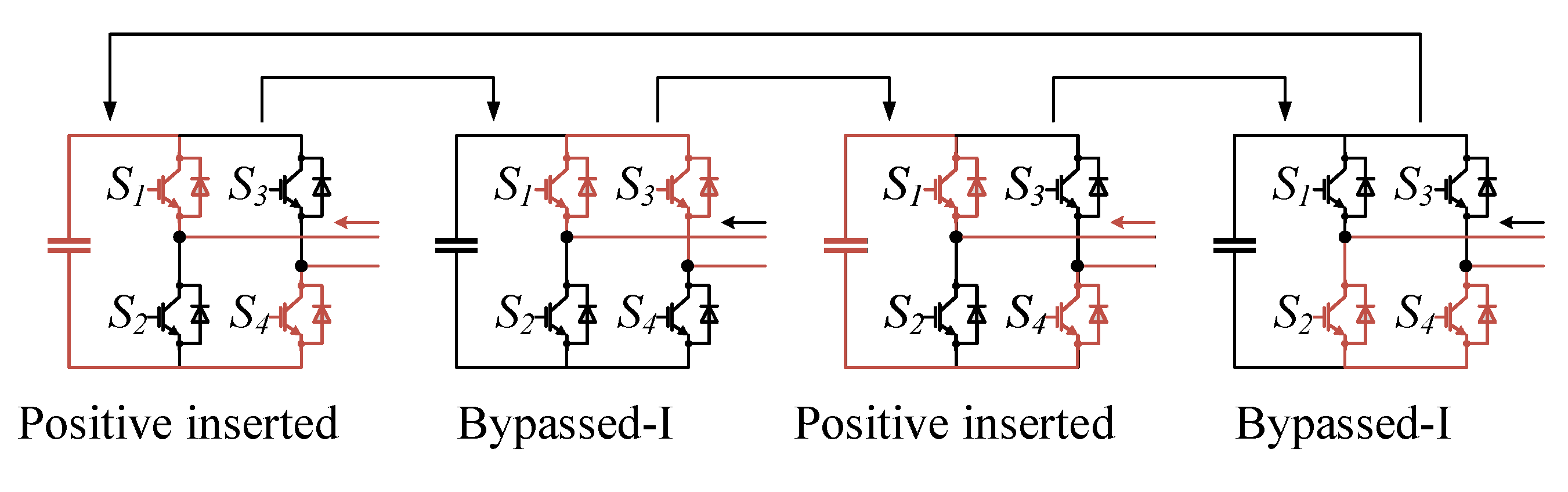
  102. Ko, Y.; Andresen, M.; Buticchi, G.; Liserre, M. Power Routing for Cascaded H-Bridge Converters. IEEE Trans. Power Electron. 2017, 32, 9435–9446. [Google Scholar] [CrossRef] [Green Version]
  103. Andresen, M.; Raveendran, V.; Buticchi, G.; Liserre, M. Lifetime-Based Power Routing in Parallel Converters for Smart Transformer Application. IEEE Trans. Ind. Electron. 2018, 65, 1675–1684. [Google Scholar] [CrossRef] [Green Version]
  104. Raveendran, V.; Andresen, M.; Buticchi, G.; Liserre, M. Thermal Stress Based Power Routing of Smart Transformer With CHB and DAB Converters. IEEE Trans. Power Electron. 2020, 35, 4205–4215. [Google Scholar] [CrossRef]
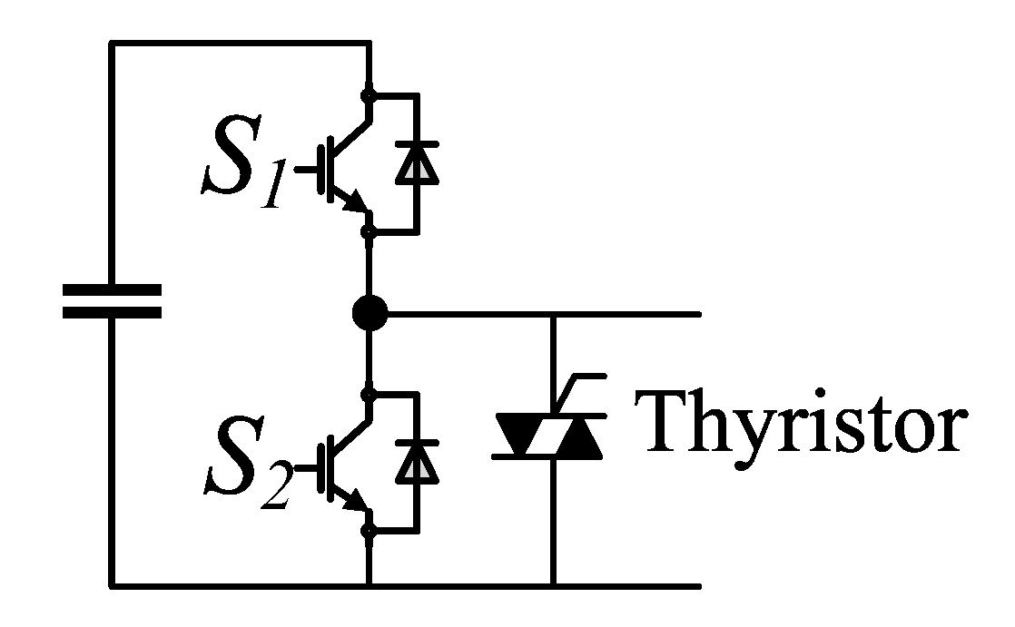
  105. Li, J. Design and Control Optimisation of a Novel Bypass-embedded Multilevel Multicell Inverter for Hybrid Electric Vehicle Drives. In Proceedings of the 2020 IEEE 11th International Symposium on Power Electronics for Distributed Generation Systems (PEDG), Dubrovnik, Croatia, 28 September–1 October 2020; pp. 382–385. [Google Scholar]
  106. Wang, J.; Liu, X.; Xiao, Q.; Zhou, D.; Qiu, H.; Tang, Y. Modulated Model Predictive Control for Modular Multilevel Converters with Easy Implementation and Enhanced Steady-State Performance. IEEE Trans. Power Electron. 2020, 35, 9107–9118. [Google Scholar] [CrossRef]
  107. Nguyen, M.H.; Kwak, S.; Kim, T. Phase-Shifted Carrier Pulse-Width Modulation Algorithm with Improved Dynamic Performance for Modular Multilevel Converters. IEEE Access 2019, 7, 170949–170960. [Google Scholar] [CrossRef]
  108. Nguyen, M.H.; Kwak, S. Nearest-Level Control Method with Improved Output Quality for Modular Multilevel Converters. IEEE Access 2020, 8, 110237–110250. [Google Scholar] [CrossRef]
  109. Gutierrez, B.; Kwak, S.-S. Modular Multilevel Converters (MMCs) Controlled by Model Predictive Control with Reduced Calculation Burden. IEEE Trans. Power Electron. 2018, 33, 9176–9187. [Google Scholar] [CrossRef]
  110. Ronanki, D.; Williamson, S.S. A Novel 2N + 1 Carrier-Based Pulse Width Modulation Scheme for Modular Multilevel Converters with Reduced Control Complexity. IEEE Trans. Ind. Applicat. 2020, 56, 5593–5602. [Google Scholar] [CrossRef]
  111. Nguyen, M.H.; Kwak, S. Simplified Indirect Model Predictive Control Method for a Modular Multilevel Converter. IEEE Access 2018, 6, 62405–62418. [Google Scholar] [CrossRef]
  112. Wang, Z.; Wang, H.; Zhang, Y.; Blaabjerg, F. Submodule Level Power Loss Balancing Control for Modular Multilevel Converters. In Proceedings of the 2018 IEEE Energy Conversion Congress and Exposition (ECCE), Portland, OR, USA, 23–27 September 2018; pp. 5731–5736. [Google Scholar]
  113. Nguyen; Kwak Switching Loss Balancing Technique for Modular Multilevel Converters Operated by Model Predictive Control Method. Electronics 2019, 8, 1175. [CrossRef] [Green Version]
  114. Sangwongwanich, A.; Mathe, L.; Teodorescu, R.; Lascu, C.; Harnefors, L. Two-dimension sorting and selection algorithm featuring thermal balancing control for modular multilevel converters. In Proceedings of the 2016 18th European Conference on Power Electronics and Applications (EPE’16 ECCE Europe), Karlsruhe, Germany, 5–9 September 2016; pp. 1–10. [Google Scholar]
  115. Hahn, F.; Andresen, M.; Buticchi, G.; Liserre, M. Thermal Analysis and Balancing for Modular Multilevel Converters in HVDC Applications. IEEE Trans. Power Electron. 2018, 33, 1985–1996. [Google Scholar] [CrossRef] [Green Version]
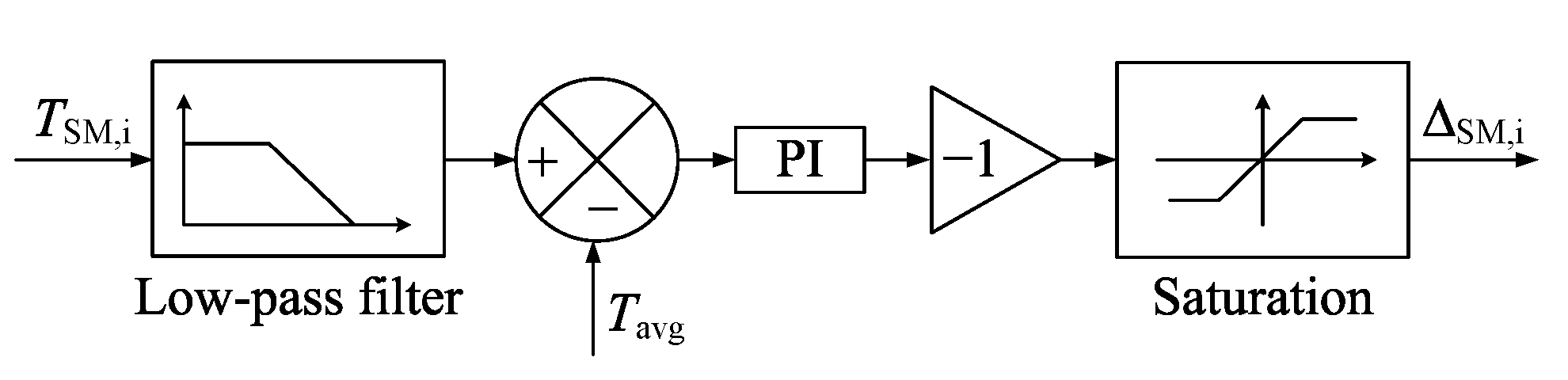
  116. Goncalves, J.; Rogers, D.J.; Liang, J. Submodule Temperature Regulation and Balancing in Modular Multilevel Converters. IEEE Trans. Ind. Electron. 2018, 65, 7085–7094. [Google Scholar] [CrossRef] [Green Version]
  117. Hagiwara, M.; Akagi, H. Control and Experiment of Pulsewidth-Modulated Modular Multilevel Converters. IEEE Trans. Power Electron. 2009, 24, 1737–1746. [Google Scholar] [CrossRef]
  118. Sheng, J.; Yang, H.; Li, C.; Chen, M.; Li, W.; He, X.; Gu, X. Active Thermal Control for Hybrid Modular Multilevel Converter Under Overmodulation Operation. IEEE Trans. Power Electron. 2020, 35, 4242–4255. [Google Scholar] [CrossRef]
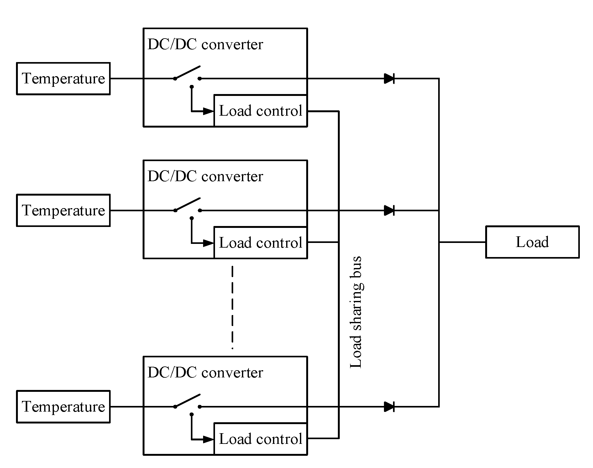
  119. Nesgaard, C.; Andersen, M.A.E. Optimized load sharing control by means of thermal reliability management. In Proceedings of the 2004 IEEE 35th Annual Power Electronics Specialists Conference (IEEE Cat. No.04CH37551), Aachen, Germany, 20–25 June 2004; pp. 4901–4906. [Google Scholar]
  120. Joseph, C.J.J.; Zolghadri, M.R.; Homaifar, A.; Lee, F.; Lorenz, R.D. Novel thermal based current sharing control of parallel converters. In Proceedings of the 2004 10th International Workshop on Computational Electronics (IEEE Cat. No.04EX915), Chicago, IL, USA, 19–23 September 2004; pp. 647–653. [Google Scholar]
  121. Barnette, J.L.; Zolghadri, M.R.; Walters, M.; Homaifar, A. Temperature Integrated Load Sharing of Paralleled Modules. In Proceedings of the 2006 1st IEEE Conference on Industrial Electronics and Applications, Singapore, 24–26 May 2006; pp. 1–6. [Google Scholar]
  122. Guerrero, J.M.; Vasquez, J.C.; Matas, J.; de Vicuna, L.G.; Castilla, M. Hierarchical Control of Droop-Controlled AC and DC Microgrids—A General Approach Toward Standardization. IEEE Trans. Ind. Electron. 2011, 58, 158–172. [Google Scholar] [CrossRef]
  123. Peyghami, S.; Mokhtari, H.; Blaabjerg, F. Decentralized Load Sharing in a Low-Voltage Direct Current Microgrid with an Adaptive Droop Approach Based on a Superimposed Frequency. IEEE J. Emerg. Sel. Top. Power Electron. 2017, 5, 1205–1215. [Google Scholar] [CrossRef] [Green Version]
  124. Peyghami, S.; Davari, P.; Blaabjerg, F. System-level lifetime-oriented power sharing control of paralleled DC/DC converters. In Proceedings of the 2018 IEEE Applied Power Electronics Conference and Exposition (APEC), San Antonio, TX, USA, 4–8 March 2018; pp. 1890–1895. [Google Scholar]
  125. Marquez, A.; Leon, J.I.; Vazquez, S.; Franquelo, L.G. Closed-loop active thermal control via power routing of parallel DC-DC converters. In Proceedings of the 2018 IEEE 12th International Conference on Compatibility, Power Electronics and Power Engineering (CPE-POWERENG 2018), Doha, Qatar, 10–12 April 2018; pp. 1–6. [Google Scholar]
  126. Yan, H.; Buticchi, G.; Yang, J.; Zhao, W.; Zhang, H.; Gerada, C. Active Thermal Control for Power Converters in Modular Winding Permanent Magnet Synchronous Motor. In Proceedings of the 2019 IEEE 13th International Conference on Compatibility, Power Electronics and Power Engineering (CPE-POWERENG), Sonderborg, Denmark, 23–25 April 2019; pp. 1–6. [Google Scholar]
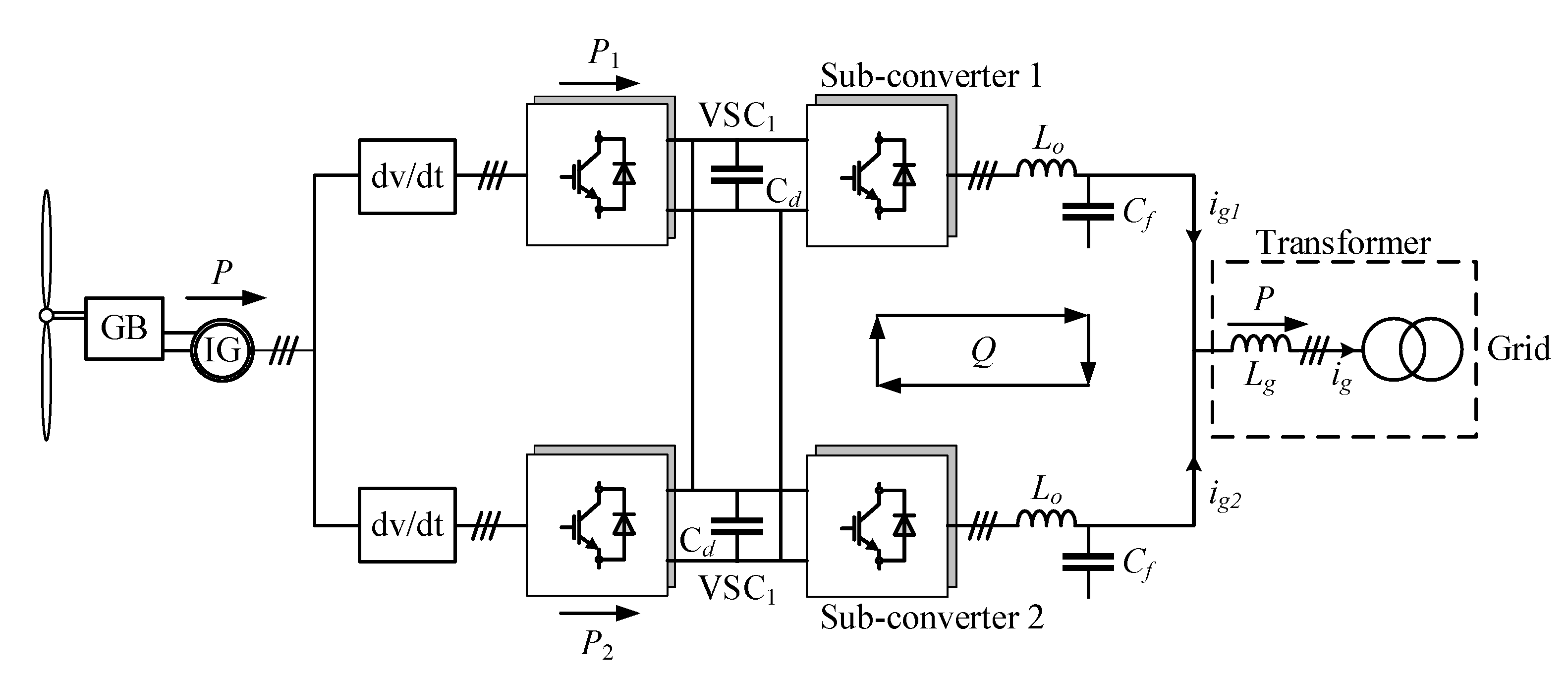
  127. Zhang, J.; Chen, G.; Cai, X. Thermal smooth control for Multi-MW parallel wind power converter. In Proceedings of the 2013 IEEE International Conference of IEEE Region 10 (TENCON 2013), Xi’an, China, 22–25 October 2013; pp. 1–4. [Google Scholar]
  128. Zhang, J.; Li, Y.; Wang, H.; Cai, X.; Igarashi, S.; Wang, Z. Thermal smooth control based on orthogonal circulating current for multi-MW parallel wind power converter. In Proceedings of the 2014 International Power Electronics and Application Conference and Exposition, Shanghai, China, 5–8 November 2014; pp. 146–151. [Google Scholar]
  129. Zhang, J.; Wang, J.; Cai, X. Active Thermal Control-Based Anticondensation Strategy in Paralleled Wind Power Converters by Adjusting Reactive Circulating Current. IEEE J. Emerg. Sel. Top. Power Electron. 2018, 6, 277–291. [Google Scholar] [CrossRef]
  130. Ma, K.; Liserre, M.; Blaabjerg, F. Reactive Power Influence on the Thermal Cycling of Multi-MW Wind Power Inverter. IEEE Trans. Ind. Applicat. 2013, 49, 922–930. [Google Scholar] [CrossRef]
  131. Ahmadzadeh, F.; Lundberg, J. Remaining useful life estimation: Review. Int. J. Syst. Assur. Eng. Manag. 2014, 5, 461–474. [Google Scholar] [CrossRef]
  132. Manson, S.S.; Dolan, T.J. Thermal Stress and Low Cycle Fatigue. J. Appl. Mech. 1966, 33, 957. [Google Scholar] [CrossRef] [Green Version]
  133. Bayerer, R.; Herrmann, T.; Licht, T.; Lutz, J.; Feller, M. Model for Power Cycling lifetime of IGBT Modules-various factors influencing lifetime. In Proceedings of the 5th International Conference on Integrated Power Electronics Systems, Nuremberg, Germany, 11–13 March 2008; pp. 1–6. [Google Scholar]
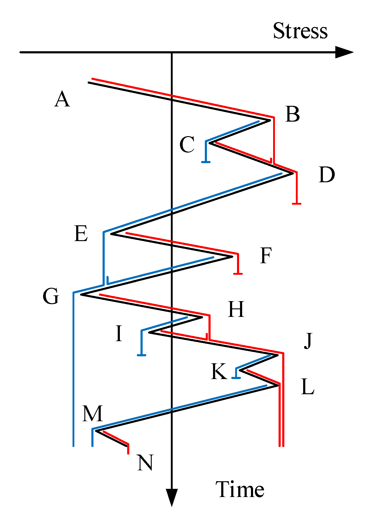
  134. Rychlik, I. A new definition of the rainflow cycle counting method. Int. J. Fatigue 1987, 9, 119–121. [Google Scholar] [CrossRef]
  135. Miner, M.A. Cumulative damage in fatigue. J. Appl. Mech. 1945, 12, A159–A164. [Google Scholar]
  136. Ma, K.; Liserre, M.; Blaabjerg, F.; Kerekes, T. Thermal Loading and Lifetime Estimation for Power Device Considering Mission Profiles in Wind Power Converter. IEEE Trans. Power Electron. 2015, 30, 590–602. [Google Scholar] [CrossRef]
  137. Ji, H.; Li, H.; Li, Y.; Yang, L.; Lei, G.; Xiao, H.; Zhao, J.; Shi, L. A Reliability Evaluation Model for the Power Devices Used in Power Converter Systems Considering the Effect of the Different Time Scales of the Wind Speed Profile. J. Power Electron. 2016, 16, 685–694. [Google Scholar] [CrossRef] [Green Version]
  138. Shipurkar, U.; Lyrakis, E.; Ma, K.; Polinder, H.; Ferreira, J.A. Lifetime Comparison of Power Semiconductors in Three-Level Converters for 10-MW Wind Turbine Systems. IEEE J. Emerg. Sel. Top. Power Electron. 2018, 6, 1366–1377. [Google Scholar] [CrossRef]
  139. Ma, K. Electro-Thermal Model of Power Semiconductors Dedicated for Both Case and Junction Temperature Estimation. In Power Electronics for the Next Generation Wind Turbine System; Research Topics in Wind Energy; Springer International Publishing: Cham, Switzerland, 2015; Volume 5, pp. 139–143. [Google Scholar]
  140. Liu, H.; Ma, K.; Qin, Z.; Loh, P.C.; Blaabjerg, F. Lifetime Estimation of MMC for Offshore Wind Power HVDC Application. IEEE J. Emerg. Sel. Top. Power Electron. 2016, 4, 504–511. [Google Scholar] [CrossRef]
  141. Kovacevic, I.F.; Drofenik, U.; Kolar, J.W. New physical model for lifetime estimation of power modules. In Proceedings of the the 2010 International Power Electronics Conference—ECCE ASIA, Sapporo, Japan, 21–24 June 2010; pp. 2106–2114. [Google Scholar]
  142. Dusmez, S.; Duran, H.; Akin, B. Remaining Useful Lifetime Estimation for Thermally Stressed Power MOSFETs Based on on-State Resistance Variation. IEEE Trans. Ind. Applicat. 2016, 52, 2554–2563. [Google Scholar] [CrossRef]
  143. Dusmez, S.; Heydarzadeh, M.; Nourani, M.; Akin, B. Remaining Useful Lifetime Estimation for Power MOSFETs under Thermal Stress with RANSAC Outlier Removal. IEEE Trans. Ind. Inf. 2017, 13, 1271–1279. [Google Scholar] [CrossRef]
  144. Ali, S.H.; Heydarzadeh, M.; Dusmez, S.; Li, X.; Kamath, A.S.; Akin, B. Lifetime Estimation of Discrete IGBT Devices Based on Gaussian Process. IEEE Trans. Ind. Applicat. 2018, 54, 395–403. [Google Scholar] [CrossRef]
Figure 1. Survey of fragile components in the power system.
Electronics 09 02068 g001
Figure 2. Relation among condition monitoring (CM), active thermal control (ATC), and remaining useful lifetime (RUL) estimation techniques in the power system.
Electronics 09 02068 g002
Figure 3. (a) insulated gate bipolar transistor (IGBT) cross section, (b) silicon carbide metal-oxide semiconductor field-effect transistor (SiC MOSFET) cross section.
Electronics 09 02068 g003
Figure 4. IGBT/Sic MOSFET package-level structure.
Electronics 09 02068 g004
Figure 5. Configuration of V c e , o n measurement circuit for upper IGBT using a depletion mode MOSFET.
Electronics 09 02068 g005
Figure 6. Configuration of t g p measurement circuit.
Electronics 09 02068 g006
Figure 7. Configuration of the V g e , t h measurement circuit.
Electronics 09 02068 g007
Figure 8. Configuration of junction temperature estimation using internal resistance.
Electronics 09 02068 g008
Figure 9. Configuration of junction temperature estimation using short-circuit with an additional bypass switch.
Electronics 09 02068 g009
Figure 10. Diagram of junction temperature estimation using a turn-off delay time circuit.
Electronics 09 02068 g010
Figure 11. Diagram of the CM thermal resistance.
Electronics 09 02068 g011
Figure 12. Configuration of the gate leakage current measurement circuit.
Electronics 09 02068 g012
Figure 13. Block diagram of spread spectrum time domain reflectometry mechanism.
Electronics 09 02068 g013
Figure 14. Configuration of the V d s sensing circuit.
Electronics 09 02068 g014
Figure 15. Adjustable gate driver voltage for: (a) R d s , s a t measurement, (b) R d s , o n measurement.
Electronics 09 02068 g015
Figure 16. Current direction in third quadrant operation.
Electronics 09 02068 g016
Figure 17. Configuration of complete CM technique.
Electronics 09 02068 g017
Figure 18. Different combinations of switching states in three-level neutral-point-clamped (3L-NPC).
Electronics 09 02068 g018
Figure 19. Redundant states and impact on switching losses and conduction losses.
Electronics 09 02068 g019
Figure 20. Diagram of ATC-based finite control set model predictive control (FCS-MPC).
Electronics 09 02068 g020
Figure 21. Principle of power routing method.
Electronics 09 02068 g021
Figure 22. The SM temperature control diagram.
Electronics 09 02068 g022
Figure 23. Single-phase hybrid MMC.
Electronics 09 02068 g023
Figure 24. Switching states arrangement when arm voltage is positive.
Electronics 09 02068 g024
Figure 25. Half-bridge submodule (HBSM) with a parallel thyristor.
Electronics 09 02068 g025
Figure 26. Thermal loading control.
Electronics 09 02068 g026
Figure 27. Parallel converter system for wind turbine applications.
Electronics 09 02068 g027
Figure 28. Typical diagram of remaining useful lifetime (RUL) estimation technique.
Electronics 09 02068 g028
Figure 29. Thermal network: (a) Cauer model, (b) Foster model, (c) Combined model.
Electronics 09 02068 g029aElectronics 09 02068 g029b
Figure 30. Example of the rainflow counting algorithm.
Electronics 09 02068 g030
Table 1. Typical failure indicators of IGBT and SiC MOSFET.
Failure TypesMechanismIndicators
IGBTSiC MOSFETIGBTSiC MOSFET
Gate oxideHigh temperature, high electric field
Threshold voltage
Gate leakage current
Miller Plateau time duration
Drain leakage current
Miller Plateau voltage amplitude
Body diode Forward voltage bias stress
On-resistance
Forward voltage
Drain leakage current
Bond wire fatigueCombination of CTE mismatch and temperature fluctuation
On-state resistance
On-state voltage
Miller Plateau time duration
Short-circuit current
Voltage between Kelvin, power source
The eddy current in bond wires
Solder layer fatigueCombination of CTE mismatch and temperature fluctuation
Junction-to-case thermal resistance
Junction temperature
Voltage change rate d V c e / d t
Current change rate d I c / d t
Low order harmonic
Solder layer resistance
Table 2. Temperature-sensitive electrical parameters (TSEPs) for junction temperature estimation.
Static parameters Collector-emitter voltage under high currents V c e , h i g h
Collector-emitter voltage under high currents V c e , l o w
Gate internal resistance R g
Short circuit current I s c
Gate-emitter voltage V g e
Dynamic parameters Threshold voltage V t h
Miller Plateau voltage V g p
Turn-on/turn off delay time t d o n / t d o f f
Publisher’s Note: MDPI stays neutral with regard to jurisdictional claims in published maps and institutional affiliations.

