Practical Controller Design of Three-Phase Dual Active Bridge Converter for Low Voltage DC Distribution System


Abstract
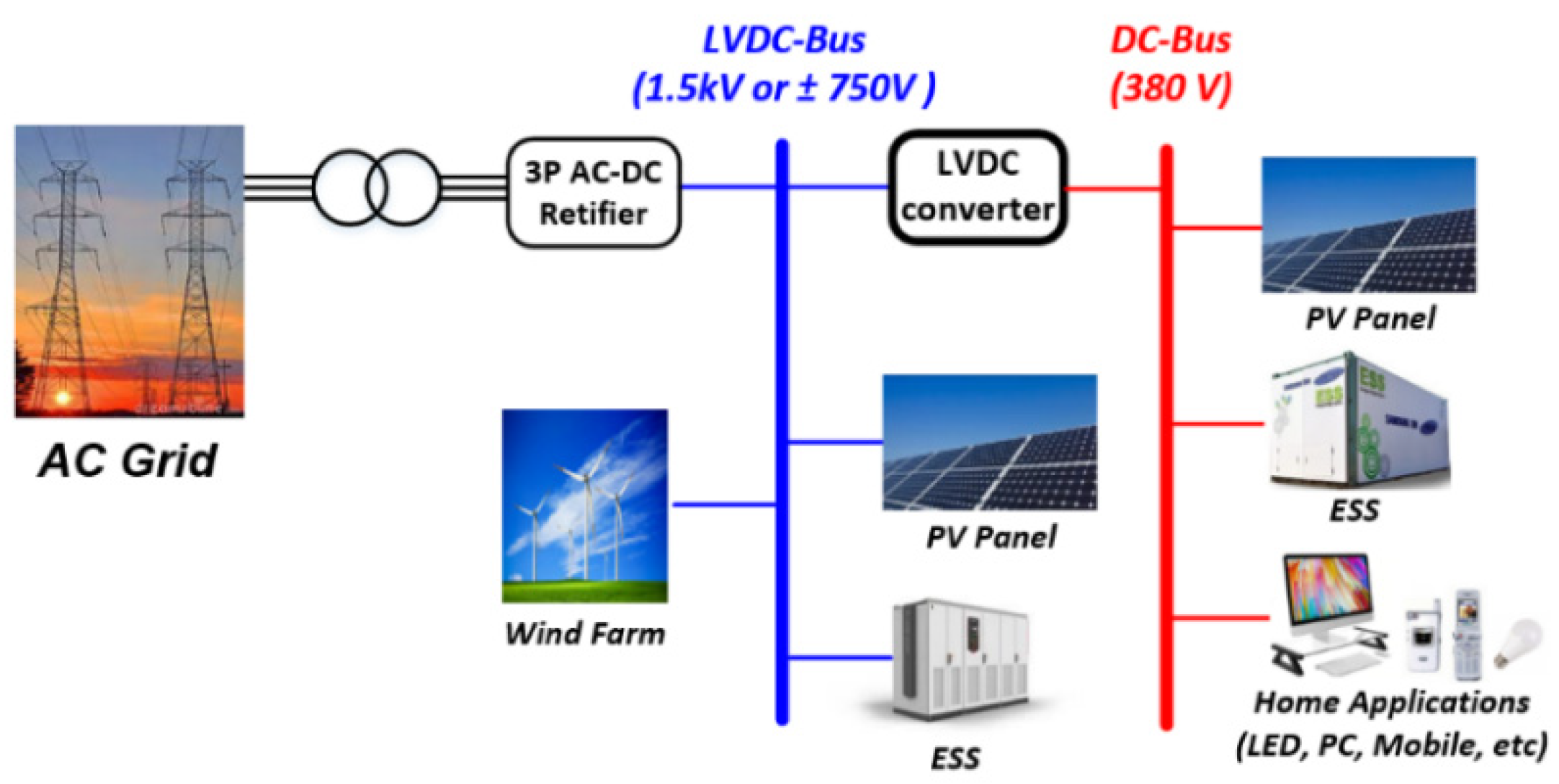
1. Introduction
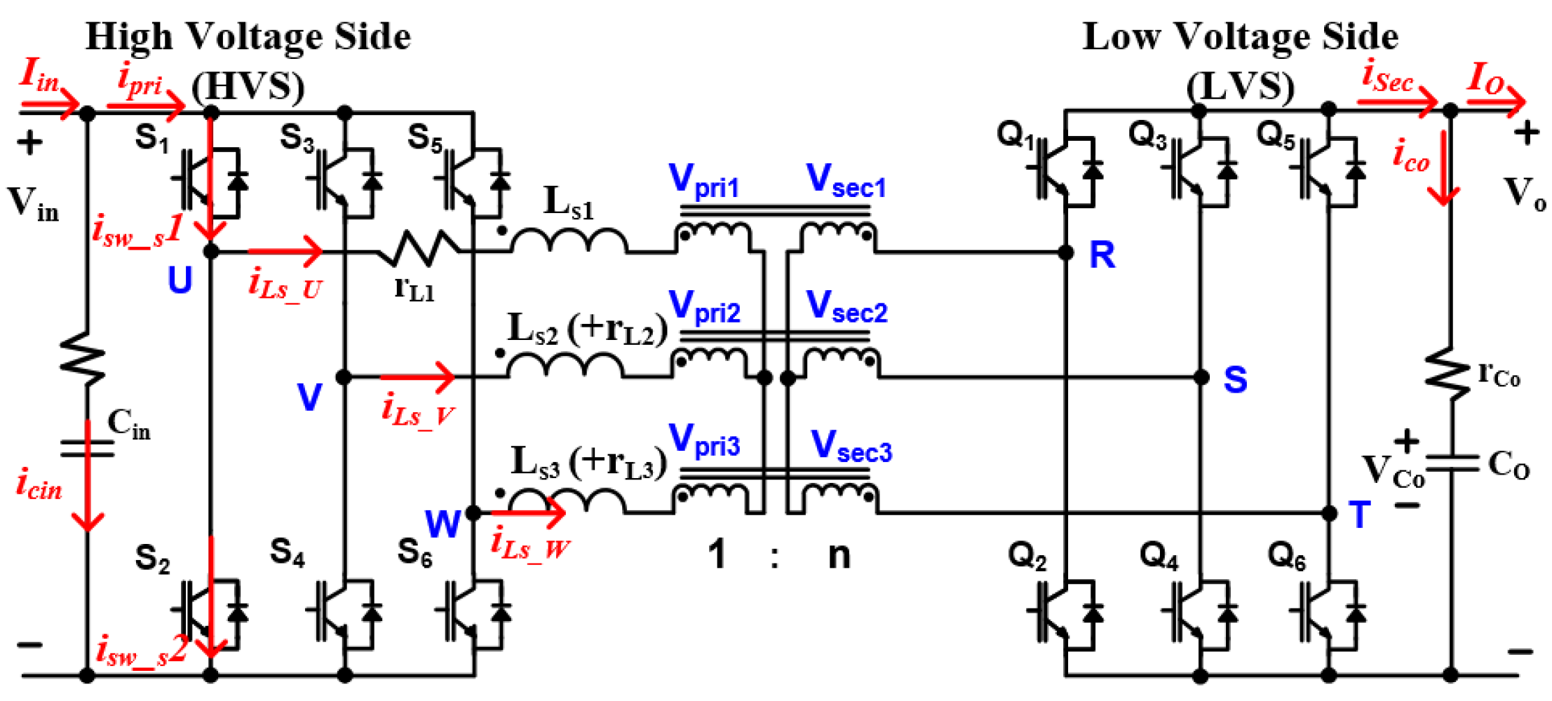
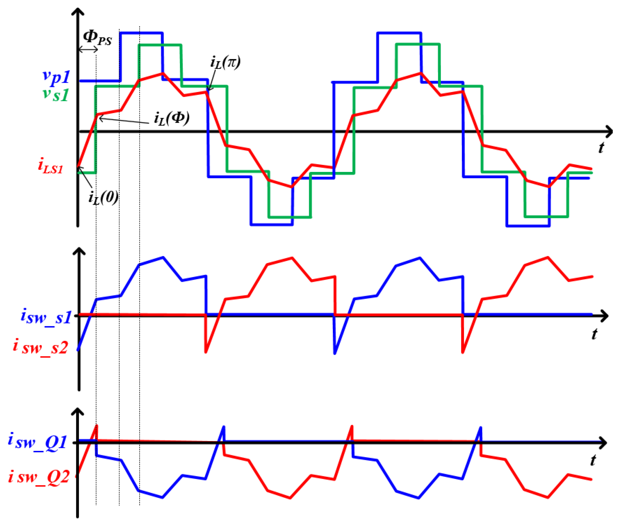
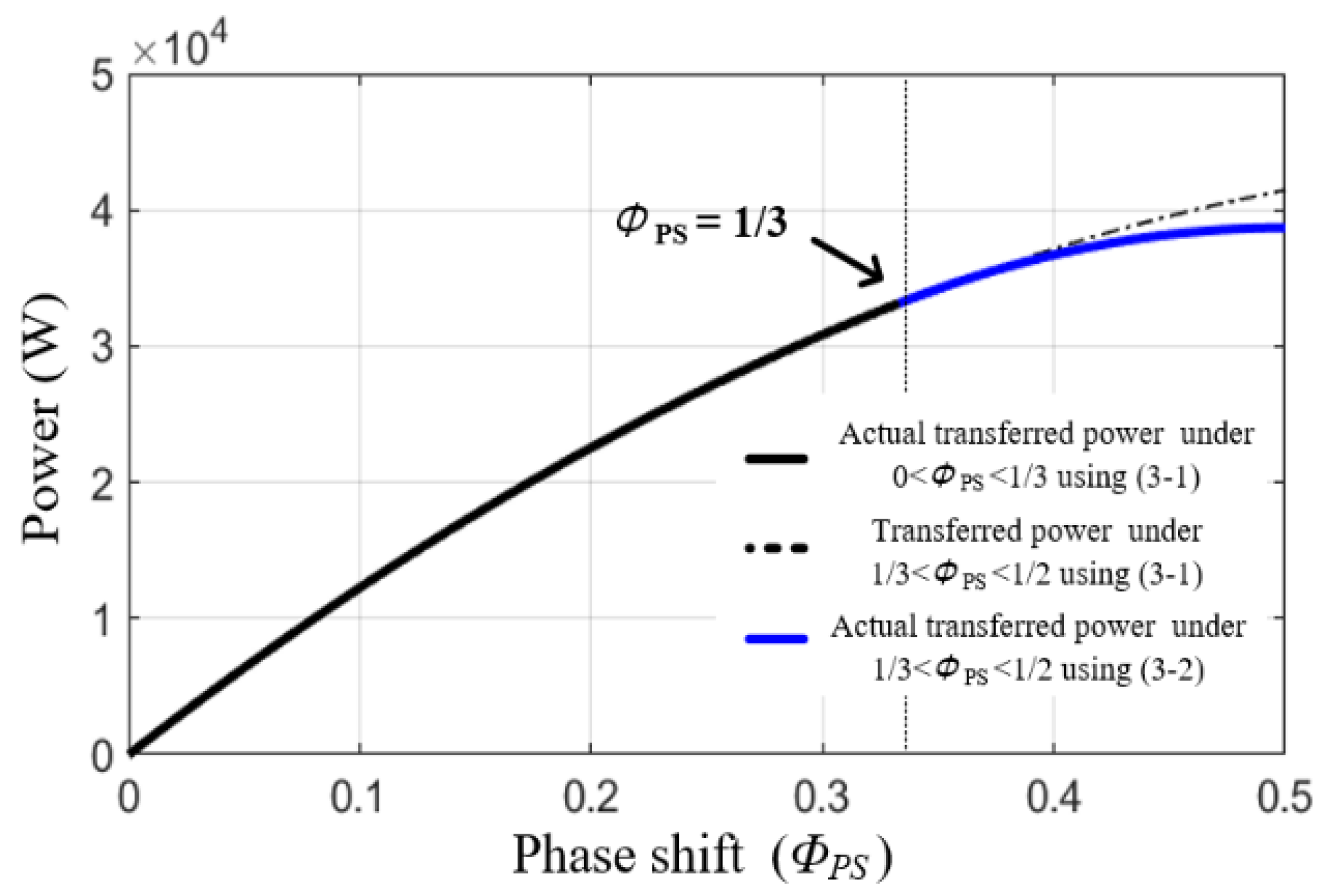
2. Operation Principles of 3P-DAB Converter
3. Design Procedure of Improved Controller
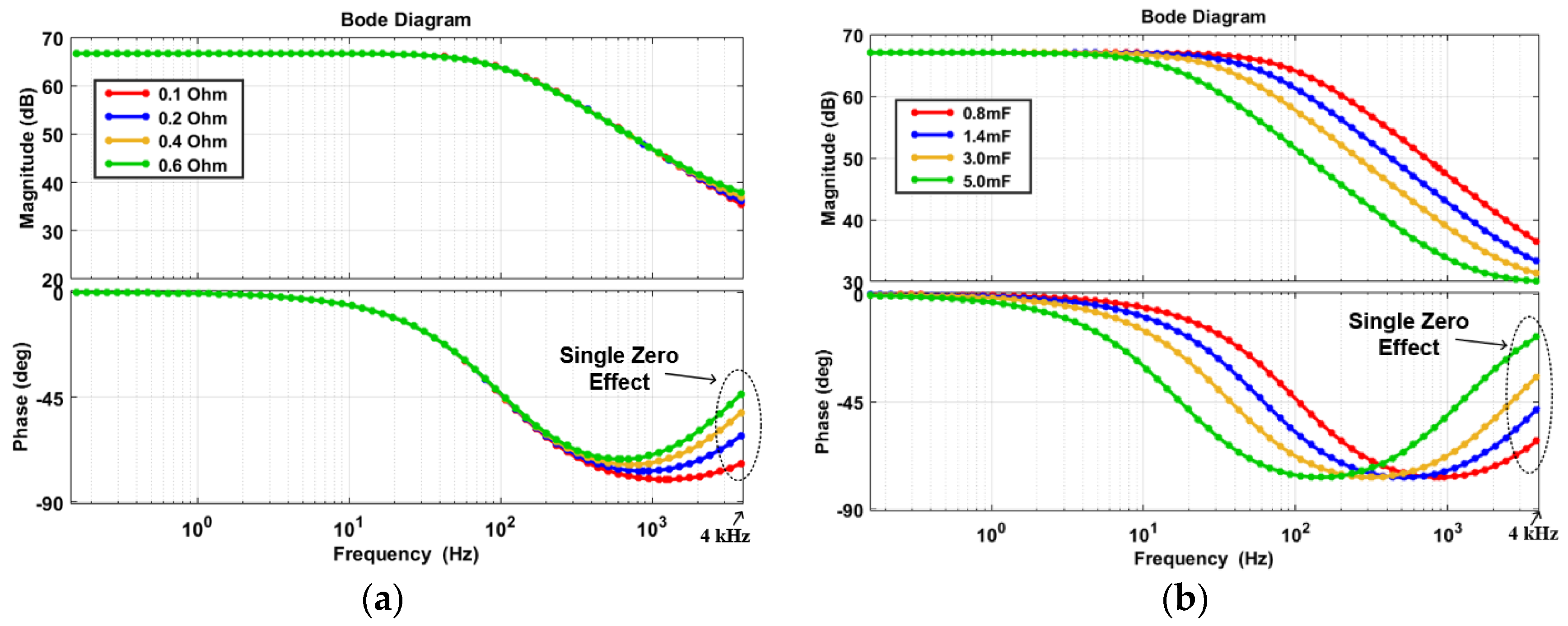
3.1. Extended Small-Signal Model
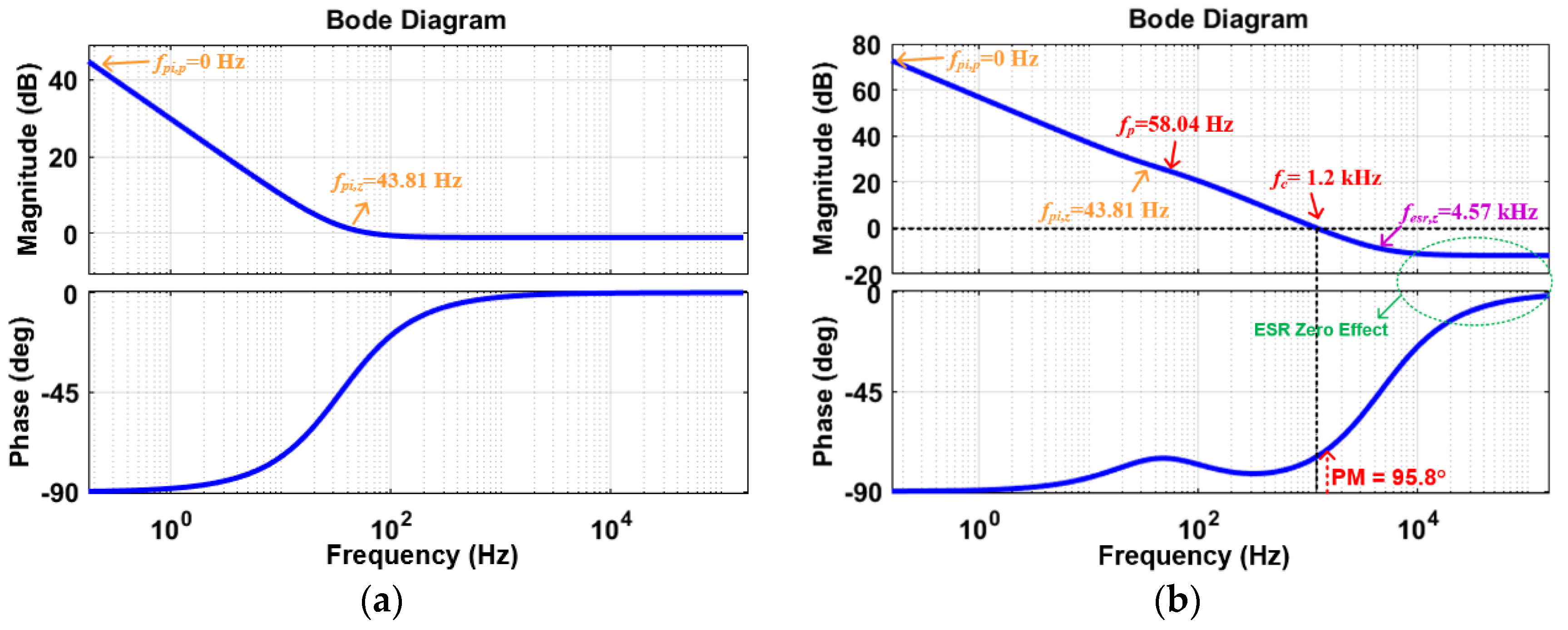
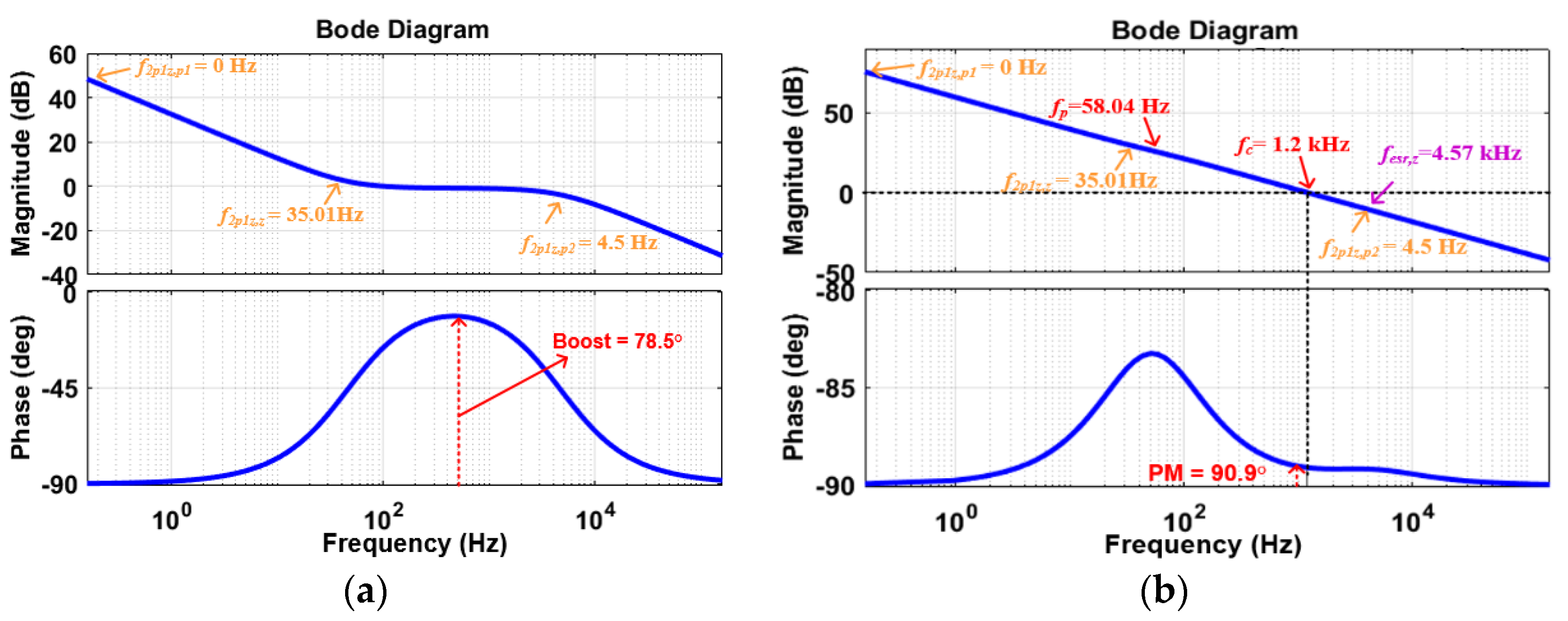
3.2. Design Strategy of Improved Controller
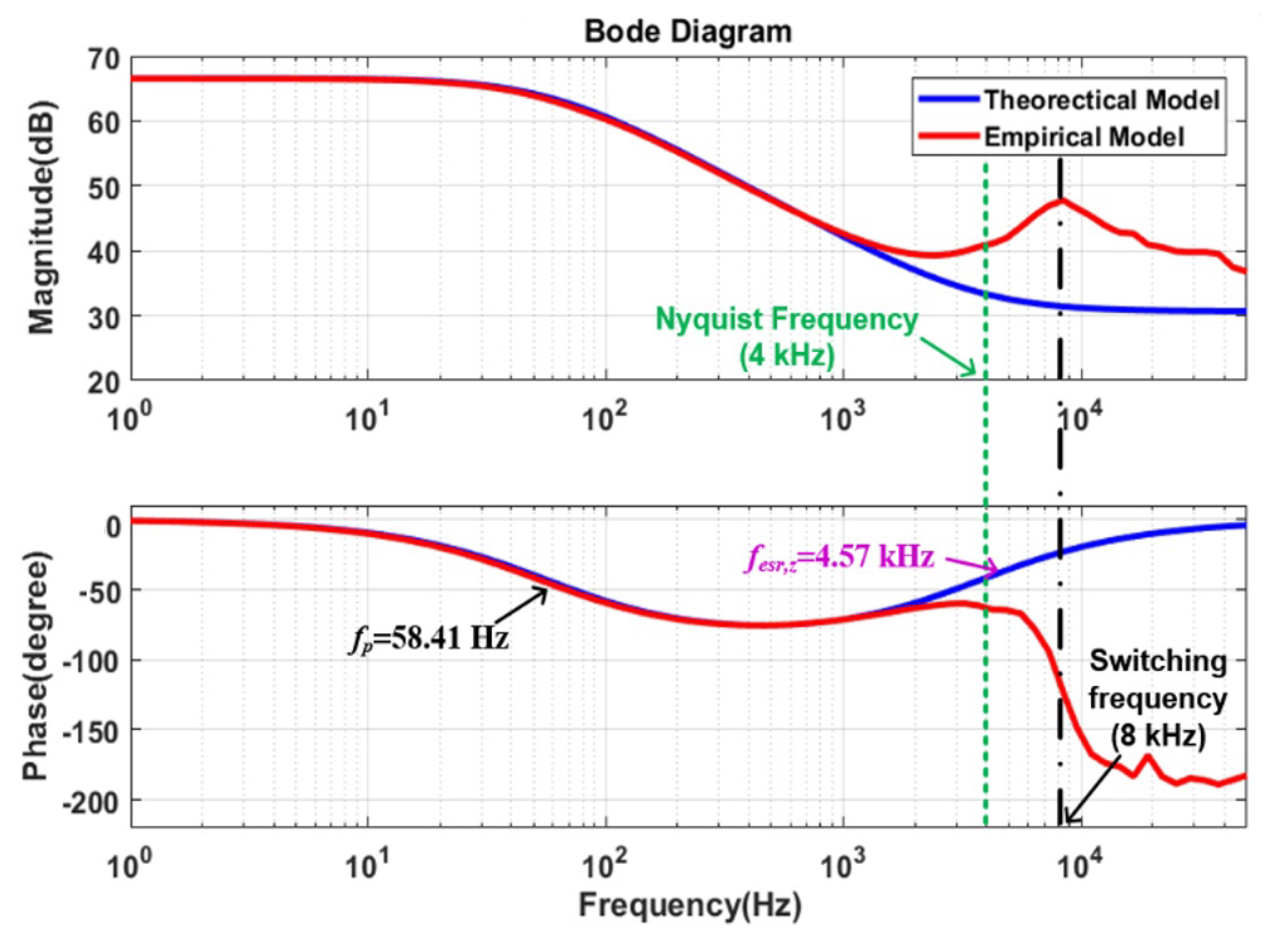
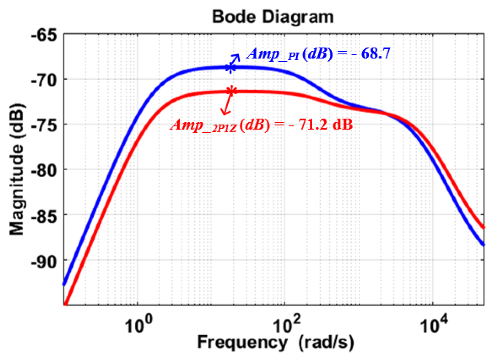
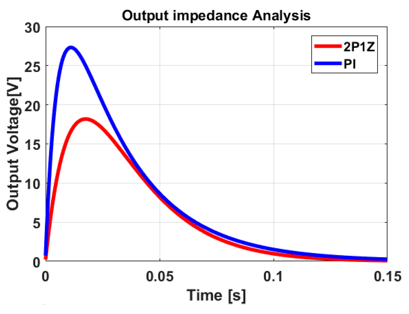
3.3. Analysis of Output Impedance
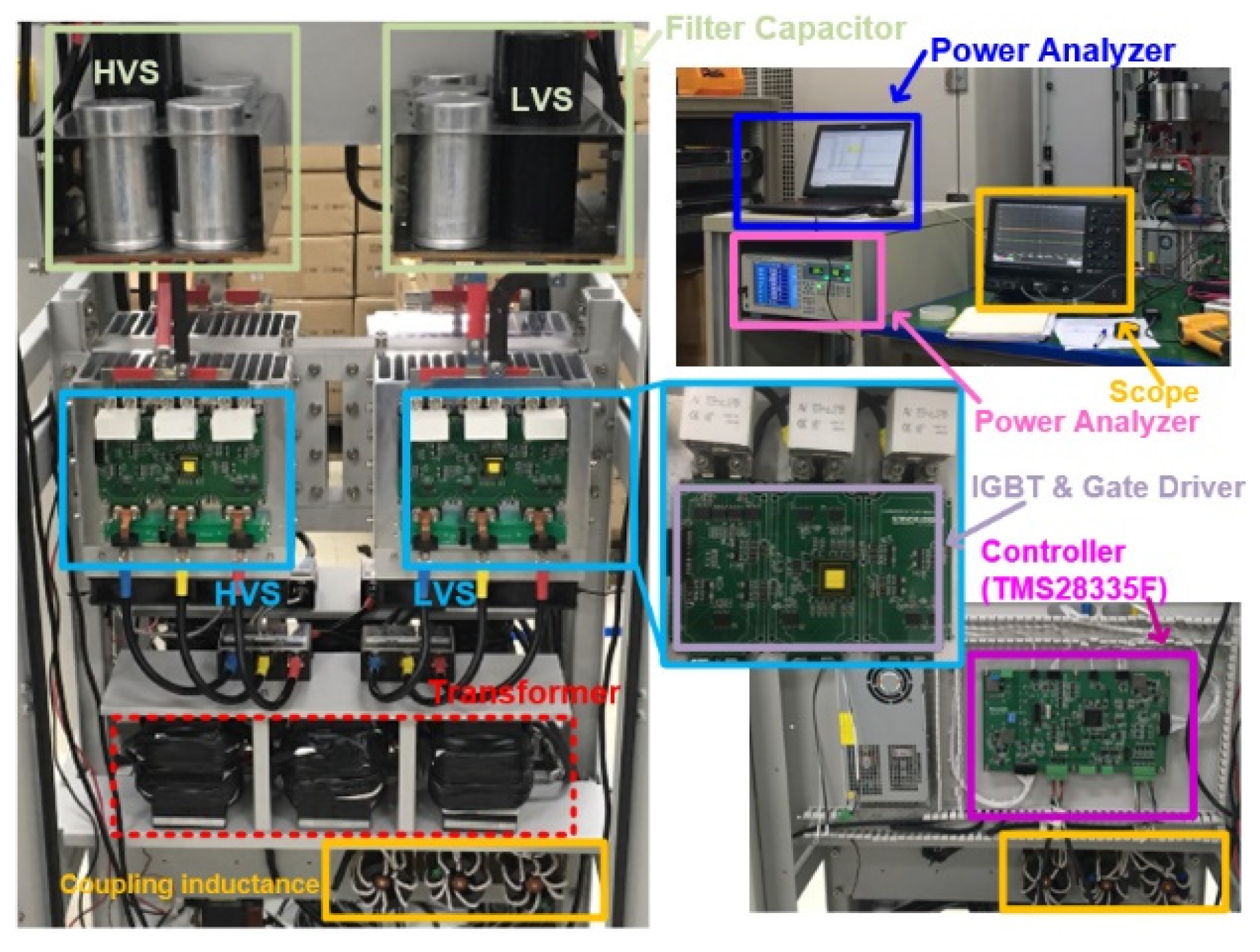
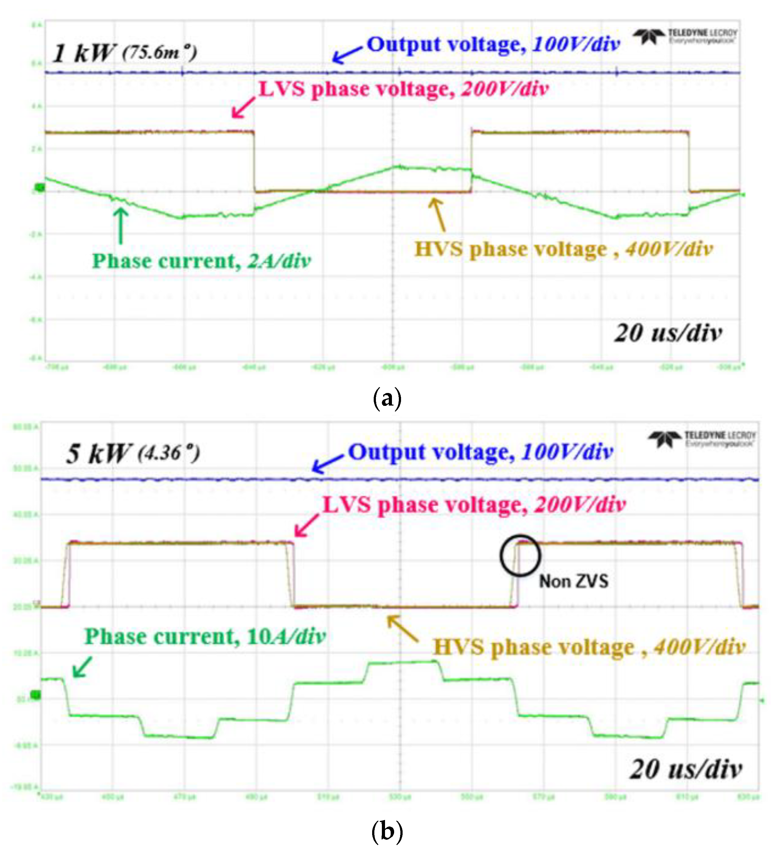
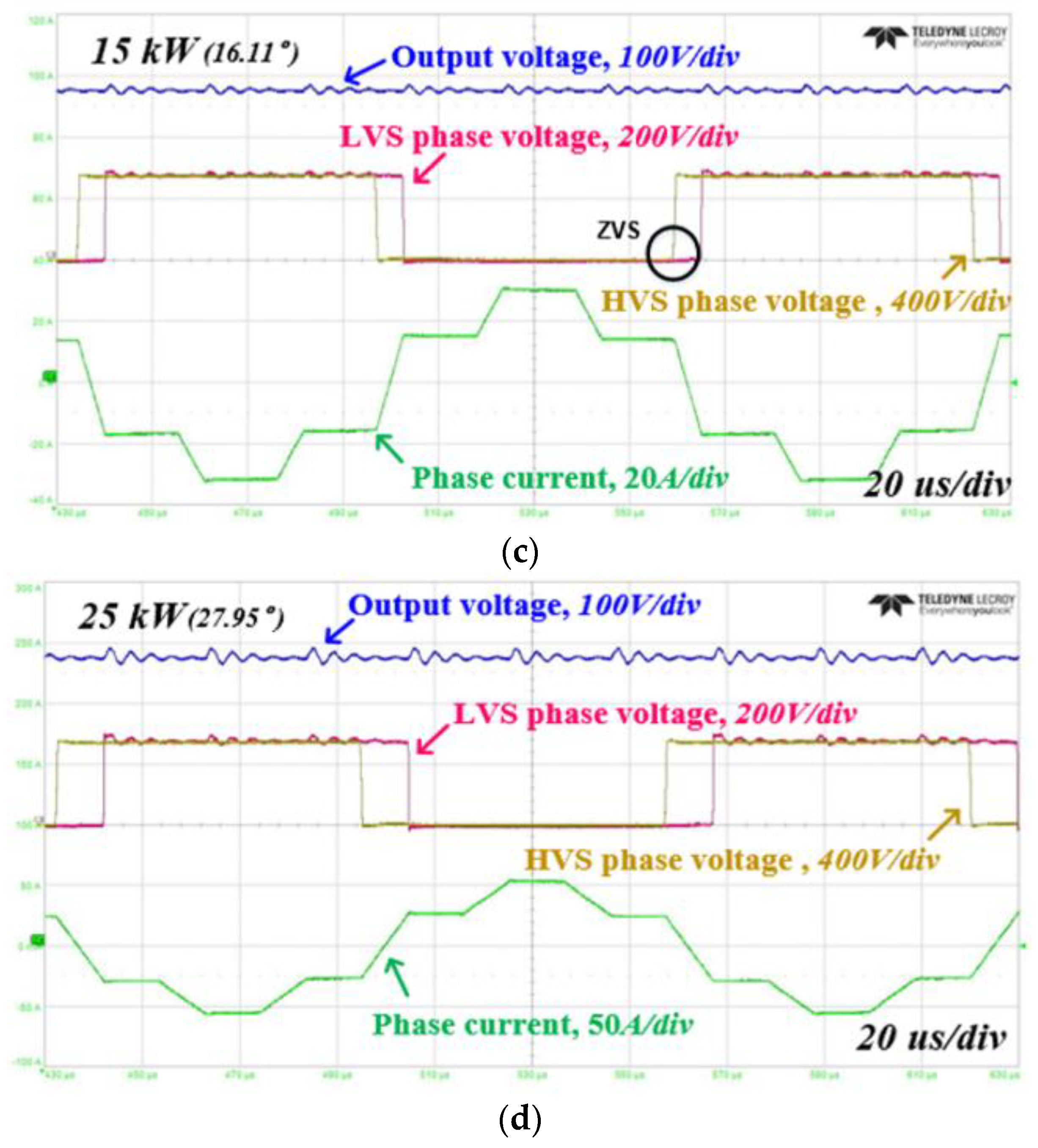
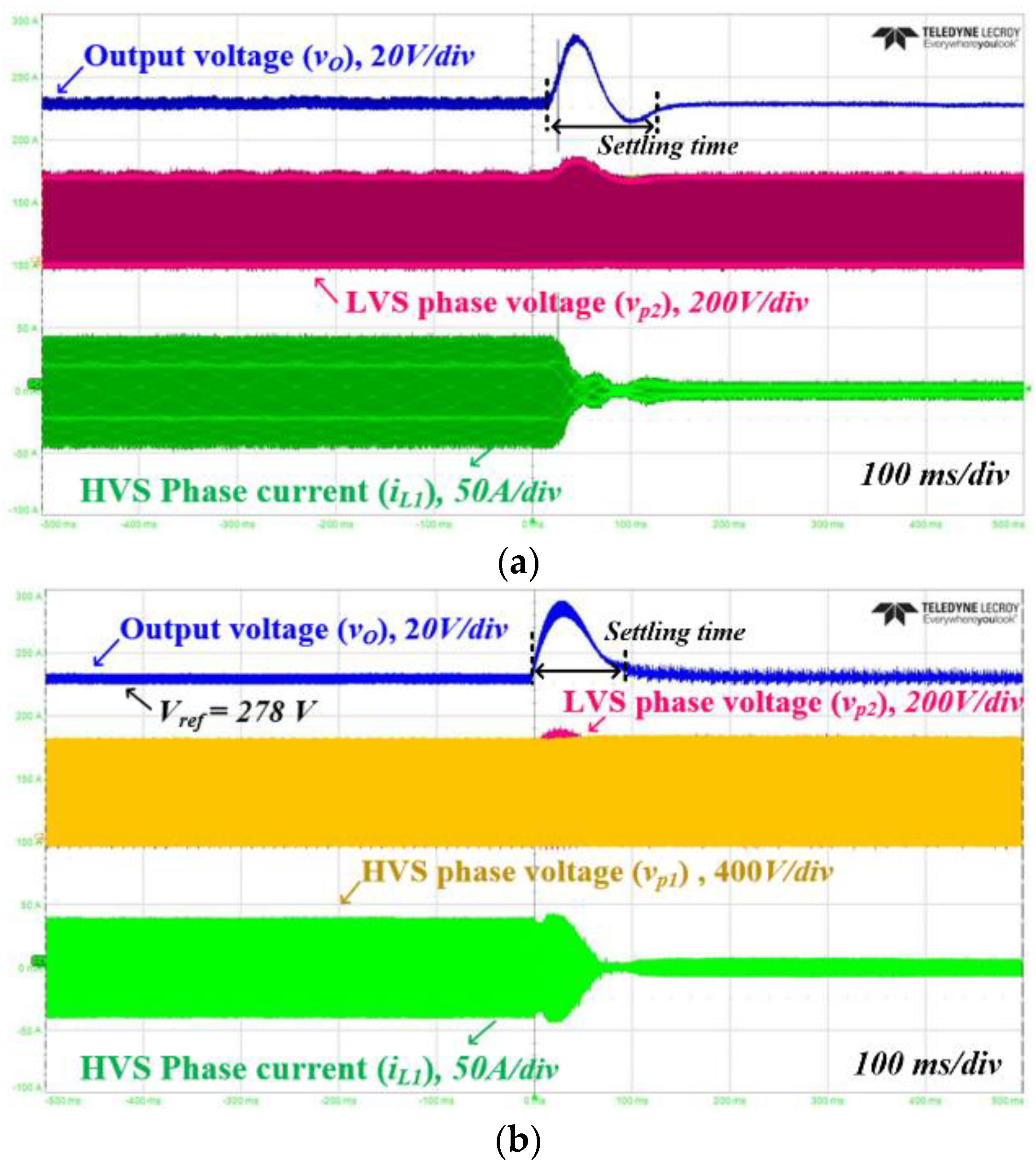
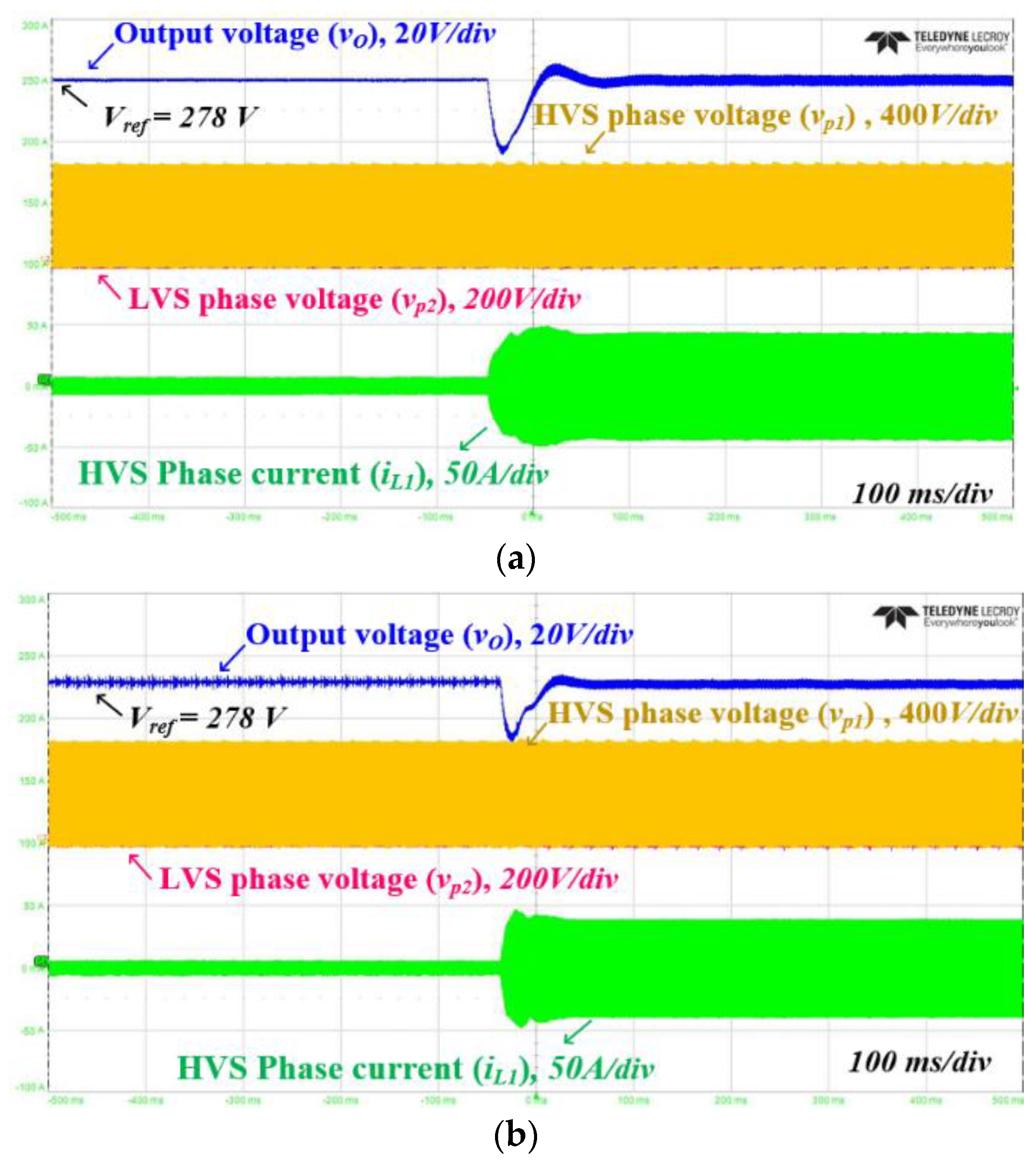
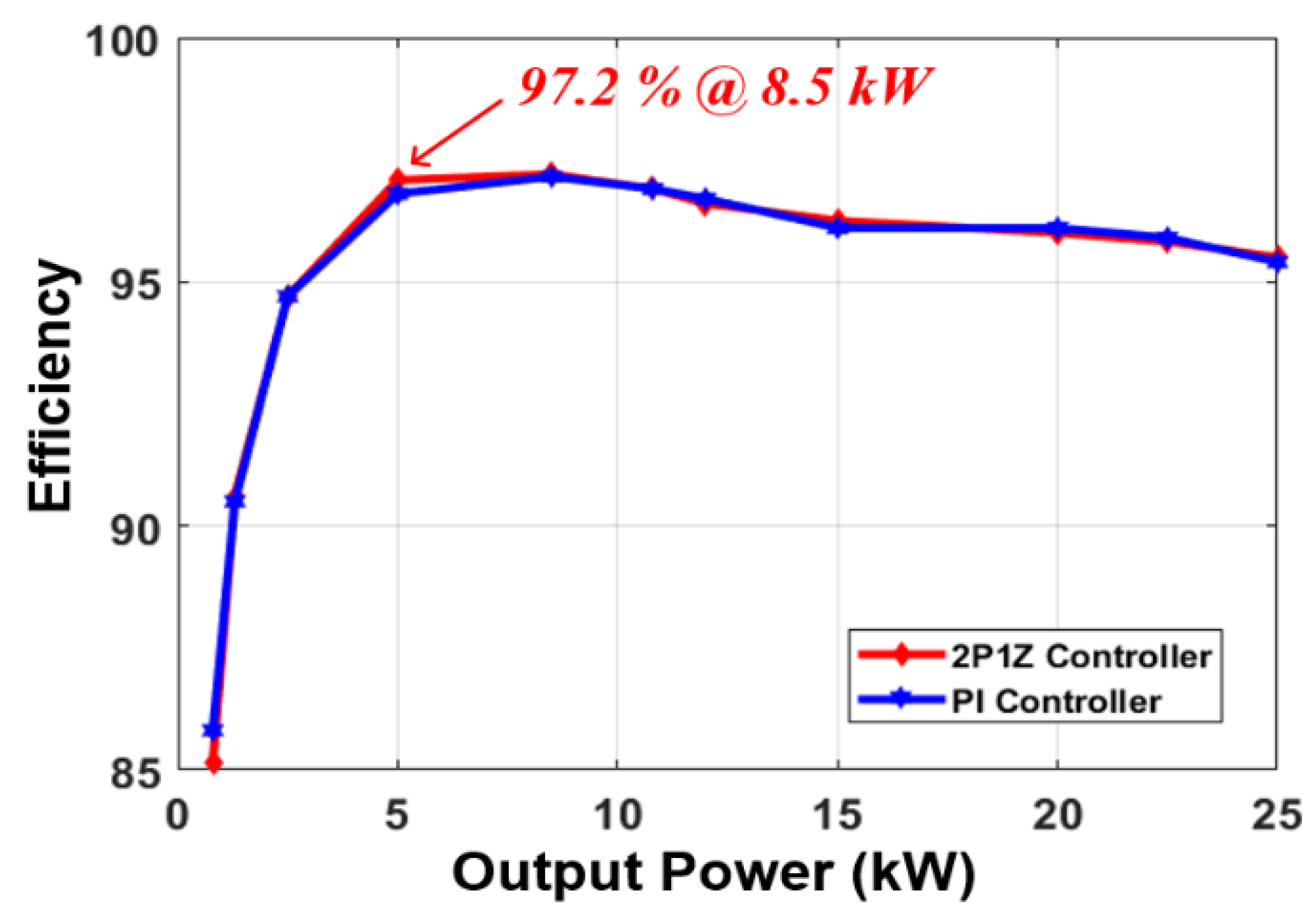
4. Experimental Results
5. Conclusions
Author Contributions
Funding
Conflicts of Interest
Nomenclature
| DC MG | direct current microgrid. |
| AC | alternating current |
| LVDC | low voltage direct current |
| IBDC | isolated bi-directional DC-DC converter |
| SP-DAB | single phase dual active bridge |
| 3P-DAB | three phase dual active bridge |
| SSM | small-signal model |
| LTI | linear time invariant |
| SPSM | single phase shift modulation |
| HVS | high voltage side |
| LVS | low voltage side |
| ZVS | zero voltage switching |
| ϕPS (=ϕ/π) | the amount of the phase shift between HVS and LVS |
| ESR | equivalent series resistance |
| SSA | state-space average |
| 2P1Z | two-pole one-zero |
| GM | gain margin |
| SPS | single phase shift |
| PM | phase margin |
Appendix A
References
- Sim, J.; Lee, J.; Jung, J. Isolated three-port DC–DC converter employing ESS to obtain voltage balancing capability for bipolar LVDC distribution system. J. Power Electron. 2020, 20, 802–810. [Google Scholar] [CrossRef]
- Heo, K.; Choi, H.; Jung, J. Real-time test-bed system development using power hardware-in-the-loop (PHIL) simulation technique for reliability test of DC nano grid. J. Power Electron. 2020, 20, 784–793. [Google Scholar] [CrossRef]
- Wang, Z.; Wang, P.; Bi, H.; Qiu, M. A bidirectional DC/DC converter with wide-voltage gain range and low-voltage stress for hybrid-energy storage systems in electric vehicles. J. Power Electron. 2020, 20, 76–86. [Google Scholar] [CrossRef]
- Jeong, D.K.; Ryu, M.H.; Kim, H.G.; Kim, H.J. Optimized design of bi-directional dual active bridge converter for low-voltage battery charger. J. Power Electron. 2014, 14, 468–477. [Google Scholar] [CrossRef]
- Choi, H.; Jung, J. Enhanced power line communication strategy for DC microgrids using switching frequency modulation of power converters. IEEE Trans. Power Electron. 2017, 32, 4140–4144. [Google Scholar] [CrossRef]
- Lee, W.; Choi, H.; Cho, Y.; Ryu, M.; Jung, J. Design methodology of a three-phase dual active bridge converter for low voltage direct current applications. J. Power Electron. 2018, 18, 482–491. [Google Scholar]
- Zhang, Z.; Xie, S.; Wu, Z.; Xu, J. Soft-switching and low conduction loss current-fed isolated bidirectional DC–DC converter with PWM plus dual phase-shift control. J. Power Electron. 2020, 20, 664–674. [Google Scholar] [CrossRef]
- Han, M.; Liu, X.; Pu, H.; Zhao, L.; Wang, K.; Xu, D. Real-time online optimal control of current-fed dual active bridges based on machine learning. J. Power Electron. 2020, 20, 43–52. [Google Scholar] [CrossRef]
- de Doncker, R.W.A.A.; Divan, D.M.; Kheraluwala, M.H. A three-phase soft-switched high-power-density DC/DC converter for high-power applications. IEEE Trans. Ind. Electron. 1991, 27, 63–73. [Google Scholar] [CrossRef]
- Choi, H.; Seo, B.; Ryu, M.; Cho, Y.; Jung, J. Effective magnetic component design of three phase dual active bridge converter for LVDC distribution system. IEEE Trans. Ind. Electron. 2020, 68, 1828–1840. [Google Scholar] [CrossRef]
- Huang, J.; Li, Z.; Shi, L.; Wang, Y.; Zhu, J. Optimized modulation and dynamic control of three-phase dual active bridge converter with variable duty cycles. IEEE Trans. Power Electron. 2019, 34, 2856–2873. [Google Scholar] [CrossRef]
- Choi, H.; Jung, J. Hybrid modulation strategy of three-phase dual-active-bridge converter to improve power conversion efficiency under light load conditions in LVDC applications. J. Power Electron. 2020, 20, 894–903. [Google Scholar] [CrossRef]
- Mi, C.; Bai, H.; Wang, C.; Gargies, S. Operation, design and control of dual h-bridge-based isolated bidirectional dc–dc converter. IET Power Electron. 2008, 1, 507–517. [Google Scholar] [CrossRef]
- Qin, H.; Kimball, J.W. Generalized average modelling of dual active bridge DC-DC converter. IEEE Trans. Power Electron. 2020, 27, 2078–2084. [Google Scholar]
- Krismer, F.; Kolar, J. Accurate power loss model derivation of a high current dual active bridge converter for an automotive application. IEEE Trans. Ind. Electron. 2010, 57, 881–891. [Google Scholar] [CrossRef]
- Zhang, Z.; Xie, S.; Shang, X.; Qian, Q.; Xu, J. Modeling and controller optimization for current-fed isolated bidirectional DC–DC converters. J. Power Electron. 2020, 20, 1592–1603. [Google Scholar] [CrossRef]
- Jiang, L.; Sun, Y.; Su, M.; Wang, H.; Dan, H. Optimized operation of dual-active-bridge DC-DC converters in the soft-switching area with triple-phase-shift control at light loads. J. Power Electron. 2018, 18, 45–55. [Google Scholar]
- Engel, S.P.; Soltau, N.; Stagge, H.; de Doncker, R.W. Dynamic and balanced control of three-phase high-power dual-active bridge DC–DC converters in DC-grid applications. IEEE Trans. Power Electron. 2013, 28, 1880–1889. [Google Scholar] [CrossRef]
- Li, Z.; Wang, Y.; Shi, L.; Huang, J.; Cui, Y.; Lei, W. Generalized averaging modelling and control strategy for three-phase dual-active-bridge DC-DC converters with three control variables. In Proceedings of the 2017 IEEE Applied Power Electronics Conference and Exposition (APEC), Tampa, FL, USA, 26–30 March 2017; pp. 1078–1084. [Google Scholar]
- Engel, S.P.; Soltau, N.; Stagge, H.; de Doncker, R.W. Improved instantaneous current control for high-power three-phase dual-active bridge DC–DC converters. IEEE Trans. Power Electron. 2014, 29, 4067–4077. [Google Scholar] [CrossRef]
- Choi, B. Pulse-Width Modulated DC-to-DC Power Conversion: Circuits, Dynamics, and Control Designs; Wiley-IEEE Press: Piscataway, NJ, USA, 2013; pp. 330–414. [Google Scholar]
- Basso, C. Designing Control Loops for Linear and Switching Power Supplies: A Tutorial Guide; Artech House: London, UK, 2012. [Google Scholar]
- Wang, J.; Xu, J.; Bao, B. Pulse bursting phenomenon in constant on-time controlled buck converter. IEEE Trans. Ind. Electron. 2011, 58, 5406–5410. [Google Scholar] [CrossRef]
- Wang, J.; Bao, B.; Xu, J.; Zhou, G.; Hu, W. dynamical effects of equivalent series resistance of output capacitor in constant on-time controlled buck converter. IEEE Trans. Ind. Electron. 2013, 60, 1759–1768. [Google Scholar] [CrossRef]
- Kwon, M.; Park, J.; Choi, S. A bidirectional three-phase push–pull converter with dual asymmetrical PWM method. IEEE Trans. Power Electron. 2016, 31, 1887–1895. [Google Scholar] [CrossRef]
- Venable, H.D. The K factor: A new mathematical tool for stability analysis and synthesis. In Proceedings of the Powercon 10, San Diego, CA, USA, 22–24 March 1983. [Google Scholar]
- Wang, T.; Yang, C. Magnetic field optimization for high-positioning-tolerant wireless charging platforms. J. Power Electron. 2020, 20, 22–33. [Google Scholar] [CrossRef]
- Avertec.Co. Soft Magnetic Core, Nanocrystalline. Available online: http://www.avertec.kr/ (accessed on 1 April 2019).
- Li, Z.; Yao, K.; Li, D.; Ni, X.; Lu, Z. Core loss analysis of Finemet type nonocrystalline alloy ribbon with different thickness. Prog. Nat. Sci. Mater. Int. 2017, 27, 588–592. [Google Scholar] [CrossRef]
- Chen, L.; Wang, Y.; Ben, T.; Yang, X.; Zhang, X.; Wang, Z. Waveform conditioning problems of nanocrystalline alloys under one/two-dimensional high-frequency magnetization. IEEE Trans. Appl. 2018, 28, 1–5. [Google Scholar] [CrossRef]
- Liu, X.; Wang, Y.; Zhu, J.; Guo, Y.; Lei, G.; Liu, C. Calculation of core loss and copper loss in amorphous/nanocrystalline core-based high frequency transformer. AIP Adv. 2016, 6, 055927. [Google Scholar] [CrossRef]


| Symbol | Quantity | Value |
|---|---|---|
| Vin | Input Voltage | 550 V |
| Vout | Output Voltage | 278 V |
| m | Voltage gain | 0.986 |
| fSW | Switching frequency | 8 kHz |
| Po,max | Rated Power | 25 kW |
| Ls,e | Effective Coupling inductance | 43.7 μH (CH740060) |
| NL | Turns | 13 |
| - | Transformer Material | Nano-crystalline |
| nP:nS | Turn ratio | 39:20 |
| RS,HVS\ | Parasitic resistor on LVS | 850 mΩ |
| RS,LVS | Parasitic resistor on HVS | 380 mΩ |
| Cof | Output filter capacitance | 1.4 mF |
| ESR | Equivalent series resistance | 138 mΩ |
| td | Dead time | 1.25 μSec |
| - | Controller | TMS320F28335 |
| P (Proportional) | I (Integration) | PI | PD | PID | ||
|---|---|---|---|---|---|---|
| Target | Reduce the transient error | Reduce the steady state error | Fast response with eliminating steady state error | Improved transient response characteristics | Improve both steady-state error and transient time | |
| Control parameter number | 1 | 1 | 2 | 2 | 3 | |
| Complexity | Low | Low | mid | Mid | high | |
| Regulation | Rough | Rough | tight | tight | Very tight | |
Publisher’s Note: MDPI stays neutral with regard to jurisdictional claims in published maps and institutional affiliations. |
© 2020 by the authors. Licensee MDPI, Basel, Switzerland. This article is an open access article distributed under the terms and conditions of the Creative Commons Attribution (CC BY) license (http://creativecommons.org/licenses/by/4.0/).
Share and Cite
Choi, H.-j.; Lee, W.-b.; Jung, J.-h. Practical Controller Design of Three-Phase Dual Active Bridge Converter for Low Voltage DC Distribution System. Electronics 2020, 9, 2101. https://doi.org/10.3390/electronics9122101
Choi H-j, Lee W-b, Jung J-h. Practical Controller Design of Three-Phase Dual Active Bridge Converter for Low Voltage DC Distribution System. Electronics. 2020; 9(12):2101. https://doi.org/10.3390/electronics9122101
Chicago/Turabian StyleChoi, Hyun-jun, Won-bin Lee, and Jee-hoon Jung. 2020. "Practical Controller Design of Three-Phase Dual Active Bridge Converter for Low Voltage DC Distribution System" Electronics 9, no. 12: 2101. https://doi.org/10.3390/electronics9122101
APA StyleChoi, H.-j., Lee, W.-b., & Jung, J.-h. (2020). Practical Controller Design of Three-Phase Dual Active Bridge Converter for Low Voltage DC Distribution System. Electronics, 9(12), 2101. https://doi.org/10.3390/electronics9122101