Abstract
In this article, a fractional-N phase-locked loop (PLL) with integrated chirp generation circuit block for a 76~81 GHz frequency-modulated continuous-wave (FMCW) radar system is presented. Thanks to the switched inductor voltage-controlled oscillator (VCO) topology, the linearity, phase noise, chirp bandwidth, and chirp rate of the FMCW synthesizer can be optimized for the short-range radar (SRR) and long-range radar (LRR) applications, with switch at ON/OFF states, respectively, according to different requirements and concerns. In this way, the proposed FMCW synthesizer shows improved phase noise for switch OFF-state, good for LRR applications, compared to the conventional single-varactor VCOs or cap-bank VCOs. The switch loss at ON-state is further decreased with the Q-boosting technique, which helps the FMCW synthesizer to simultaneously obtain a wide chirp bandwidth, steep modulation rates and good phase noise for SRR applications. The FMCW synthesizer is fabricated in 0.13 µm SiGe BiCMOS technology, occupies an area of 1.7 × 1.9 mm2, and consumes 330 mW from a 3.3 V voltage supply. Measured results show that the FMCW synthesizer can cover 25.3~27 GHz (with a frequency tripler to fully cover 76~81 GHz band), showing optimized phase noise, chirp bandwidth, linearity, and modulation rates performance. The measured K-band phase noise is −110.5 dBc/Hz for switch OFF-state, and −106 dBc/Hz for switch ON-state at 1 MHz offset. The normalized root mean square (RMS) frequency error is 518 kHz for chirp rate of ±14.6 MHz/μs and 1.44 MHz for chirp rate of ±39 MHz/μs for the 77 GHz band. Moreover, the integrated waveform generator offers fully programmability in chirp rate, duration and bandwidth, which supports multi-slope chirp generations. With a frequency tripler, the chip is well suited for the 76~81 GHz FMCW radar system.
1. Introduction
Recently, miniaturized low-cost frequency-modulated continuous-wave (FMCW) radars are becoming dominant in a range of applications, including automotive, industrial and consumer electronics. Advances in integration levels of millimeter-wave radars allowed both price reduction and size miniaturization [1]. For better measurement of close-proximity objects and their relative velocities, FMCW radars need to have both high bandwidth (to improve spatial resolution) and steep modulation rates (to push the beat tones to higher frequencies). For example, for short-range radar (SRR) applications, 4 GHz chirp bandwidth (77 to 81 GHz) can be used to differentiate objects that are only a couple of centimeters apart. To avoid baseband flicker noise, and to permit measurements of reasonably large speeds, high modulation rates should be supported. Meanwhile, the chirp linearity and phase noise are the primary determinants for long-range radar (LRR) applications (>200 m), for which 76 to 77 GHz is frequently the operational band. Poor linearity will degrade FMCW radar range resolution and accuracy as well as reduce the maximum range. Phase noise will translate directly into the system noise floor of the radar, further decreasing the maximum range. Overall, for the FMCW source, the linearity and phase noise requirements are more stringent for 76~77 GHz band, while chirp bandwidth and modulation rates are of more concern for the 77~81 GHz band [2,3,4,5].
The reported FMCW sources mostly utilize one voltage-controlled oscillator (VCO) core to fully cover 76~81 GHz for wide chirp bandwidth, which often degenerates the linearity and phase noise performance for LRR band (76~77 GHz) [3]. To obtain a wide chirp bandwidth, steep modulation rates for the FMCW source without sacrificing chirp linearity and phase noise, VCOs with multiple oscillating cores or cap-banks can be utilized [5,6,7,8]. However, multiple-core VCOs need a complex design procedure, as well as to consume more chip area and power. Cap-bank VCOs tend to have the worst phase noise performance at the lowest sub-band, when all the cap-bank switches are at ON-state (introducing the most loss due to switch ON-resistance). Then, the phase noise performance will be compromised for the low-end band (76~77 GHz), decreasing the targets detection range for LRR applications. On the contrary, VCOs using switched inductors have the best phase noise performance at the lowest sub-band, when the switch is at OFF-state. To further decrease the switch loss at ON-state, the quality-factor (Q)-boosted switched inductor technique has been introduced to implement wide-band, low-phase-noise VCO [9]. At millimeter wave frequencies, a VCO will suffer from high phase noise due to poor transistor gain as well as the low-quality factor of varactors. Therefore, combining a lower fundamental frequency VCO with a frequency multiplier can be a more appropriate solution than the direct mm-wave oscillation for the low phase noise performance [8], [10].
In this article, the design of the K-band frequency synthesizer for 77 GHz FMCW radar sensor based on a Q-boosted switched inductor VCO is presented. The proposed FMCW source has the following improvements compared to the previous reported works. Firstly, thanks to the switched inductor topology, the chirp bandwidth, modulation rate, linearity, and phase noise of the FMCW synthesizer can be optimized for SRR and LRR applications, respectively, according to different prior requirements and concerns. By this means, the VCO has the lowest phase noise and more linear tuning gain, Kvco, at low-end of tuning band when the switch is at OFF-state, which is good for LRR applications. Secondly, a wide frequency tuning range and high chirp rate can be obtained when the switch is at ON-state, suitable for SRR applications. Thirdly, the switch loss of ON-resistance is further decreased with the Q-boosted switched inductor technique, which helps to obtain wide chirp bandwidth, steep modulation rates without compromising too much phase noise for SRR applications. In this way, wide chirp bandwidth, steep chirp rates, highly linearity, and low phase noise for both LRR and SRR applications can be achieved simultaneously. The FMCW synthesizer is fabricated in a 0.13 µm SiGe BiCMOS process. Measured results have approved the design ideas.
2. Design and Implementation of the K-Band FMCW Frequency Synthesizer Using Q-Boosted Switched Inductor VCO
The block diagram of the K-band FMCW frequency synthesizer is shown in Figure 1. Considering the system implementation issues, such as the VCO performance, harmonic frequency suppression, DC power consumption, etc., the 77 GHz FMCW source can be obtained with the proposed K-band fractional-N PLL, and a frequency tripler. Instead of using VCOs with single-varactor, multiple cores, or cap banks, the proposed FMCW source has integrated the Q-boosted switched inductor VCO, which is designed with SiGe heterojunction bipolar transistor (HBT) devices for low noise. The prescaler is also implemented with HBTs for high speed performance in K-band. The phase-frequency detector (PFD), charge pump (CP) and band gap (BG)/low dropout regulators (LDOs) are designed with thick-gate-oxide CMOS transistors, and the programmable divider, the FMCW waveform generator, 20-bit multistage noise shaping (MASH) 1-1-1 sigma-delta modulator (SDM), serial-peripheral interface (SPI) circuits are designed with thin-gate-oxide CMOS transistors, both offered by the 0.13 μm SiGe BiCMOS technology. The on-board loop filter (LPF) is not integrated to the chip, for flexibility and saving chip area. The synthesizer can generate chirps with programmable bandwidth and modulation time, allowing up to 32 different chirp settings within a single modulation frame. This allows for very broad applications and implementations of different ghost target avoidance techniques [3,11].
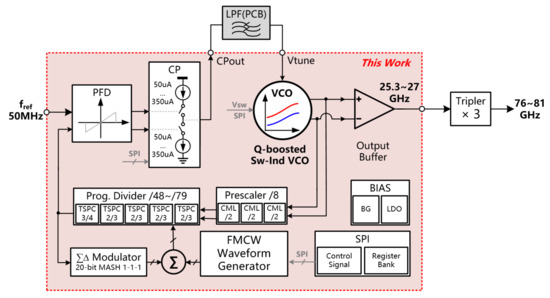
Figure 1.
Block diagram of the K-band frequency synthesizer for 77 GHz frequency-modulated continuous-wave (FMCW) radar sensor.
2.1. Voltage-Controlled Oscillator Using Q-Boosted Switched Inductor
The utilized Q-boosted switched inductor VCO in this article is based on our previous work [9]. Figure 2a shows the schematic of the K-band Colpitts VCO and equivalent circuits of the switched inductor at switch ON and OFF states. The switched inductor consists of 1:2 inductor-loaded transformer and NMOS transistor as RF switch, which is connected to the secondary coil and controlled by Vsw. LP and LS are the self-inductances of the primary and secondary coil, k is the coupling coefficient. RSoff, CSoff, YPon and CPon are the equivalent circuit parameters for the NMOS switch at OFF/ON state. Based on the transformer theory and topology [12,13,14], the detailed design procedure and Q-boosting mechanism of the switched inductor can be found in [9]. Figure 2b,c show the top view and 3-D view of the Q-boosted switched inductor with 1:2 inductor-loaded transformer. Instead of implementing the two-turn secondary coil on the same metal layer in [9], the two-turn coil is realized in stack layout for higher inductor switching ratio. To reduce the parasitic capacitance between inductors, the stack two-turn secondary coil is not fully overlapped. A wide metal width of 10 μm is chosen for all coils. In addition, the primary inductor is realized on the top metal layer with thickness of 4 μm. The secondary inductor is placed on top and second metal layers with thickness of 4 and 1.42 μm, to reduce the series loss and get a higher quality factor for the inductors. Full-wave EM simulation is used in the Q-boosted switched inductor design. The simulated Q of the switched inductor Leq is 20 for switch OFF-state and 14 for switch ON-state at 25 GHz. In the K-band Colpitts VCO, the LC tank consists of C1, C2, L2, Cvar, Le, and Leq. Cvar is capacitance of the varactor, which is biased with tuning voltage, Vt. Bipolar transistors T1 and T2 generate the desired negative resistance to sustain oscillation. The biasing condition for T1~T4 is optimized for noise and output power. The emitter lengths for T1,2 and T3,4 are 18 µm and 10 µm, respectively. The switching inductor signal, Vsw, is controlled by on-chip SPI.
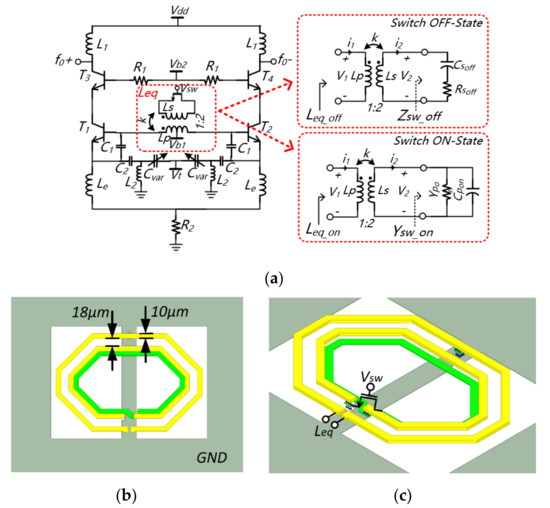
Figure 2.
(a) Schematic of the Colpitts voltage-controlled oscillator (VCO), and equivalent circuits of switched inductor at switch ON/OFF state; (b) top view of the Q-boosted switched inductor; (c) 3-D view of the Q-boosted switched inductor with 1:2 inductor-loaded transformer.
2.2. Prescaler and Programmable Divider
The prescaler consists of three current mode logic (CML) divide-by-2 stages [9], as shown in Figure 3a, which divides the K-band VCO output to ~3.2 GHz signal. The CML divider has the advantages of small area and wider operation bandwidth, compared to the injection-locked frequency divider (ILFD). Circuit parameters are optimized for each CML stage to get a better RF performance and lower power consumption for input signals around ~26/~13/~6.5 GHz. The programmable divider includes four stages of true single-phase clock (TSPC) divide-by-2/3 cells, followed by one stage of a divide-by-3/4 cell, as shown in Figure 3b. The divide-by-2/3 cell and divide-by-3/4 cell are shown in Figure 3c,d, respectively. Between the SDM outputs and programmable divider control inputs, additional D-type flip-flops and logic gates are placed to eliminate wrong settings due to a glitch or a synchronous failure in the system.
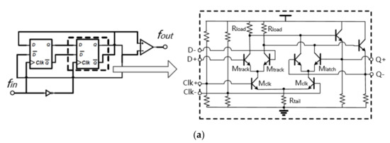
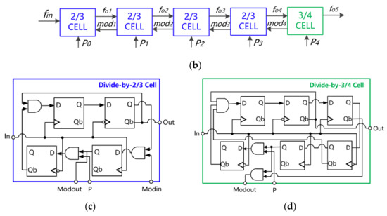
Figure 3.
Schematic of the (a) current mode logic (CML) divide-by-2 divider and (b) 5-bit true single-phase clock (TSPC) programmable frequency divider; (c) divide-by-2/3 cell; (d) divide-by-3/4 cell.
2.3. Phase-Frequency Detector and Charge Pump
The PFD compares the reference signal, Fref, and the divided signal, Fdiv, and controls the CP current according to the phase and frequency difference, as shown in Figure 4a. The charge pump needs to provide matched up and down currents for most of the CP output voltage range. The charge pump architecture employs dual operation amplifiers (Op-amps) where both amplifiers utilize a high swing topology [15]. The first amplifier acts as a unity gain amplifier to track the change of VCO control (cpout) node to the dummy node, while the second amplifier forms the feedback loop where the gate voltage of PMOS in the up current path is tracked to keep the current the same as that of NMOS. Using this technique, good matching between up and down currents can be obtained. Op-amps also suppress the supply noise and reference spurs. Hence the operation around the supply/ground edge is the worst case scenario as the Op-amp gain is reduced, which should be avoided in the CP output voltage range. The CP includes three binary weighted branches so that the current can be digitally controlled from 50 μA to 350 μA, adapting the PLL’s loop bandwidth/settling time for various chirp configurations.
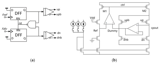
Figure 4.
Schematic for (a) the phase-frequency detector; (b) the charge pump with dual Op-amp design for matching up and down currents.
2.4. FMCW Multichirp Generator and Sigma Delta Modulator
The architecture of the FMCW multi-chirp generator in [3] has been employed in this work. The building blocks include programmable chirp data queue, frequency step generator, time step generator, frequency step integrator, chirp timing generator, chirp selection, frequency initialization, etc. A 20-bit MASH 1-1-1 SDM is used for fine adjustment of chirp frequency step. All of the 32 available chirp settings are loaded directly from the SPI register bank, which allows generation of programmable chirp arrays. Thus, the chirp configuration is more flexible, compared to the circuits operating with pre-defined and hard-wired control settings. One issue in fractional-N PLLs for FMCW radar applications is the occurrence of glitches at the output frequency. This results in the fractional part of the division ratio propagating through the accumulators of SDM, while the integer part directly arrives at the input of the adder responsible for driving the programmable divider. This problem can be solved by introducing extra delays to the integer part of the control code [16].
3. Results
The proposed K-band FMCW frequency synthesizer with a Q-boosted switched inductor VCO and an integrated multi-chirp generator is implemented using 0.13 µm SiGe BiCMOS technology. The top metal and second metal with thickness of 4 and 1.42 µm are used in the design of RF signal interconnections/passive parts, as well as the power routing, while the third metal with thickness of 0.6 µm is used as the RF/DC ground. The K-band FMCW frequency synthesizer chip is wire-bonded to the printed-circuit-board (PCB), on which the PLL’s loop filter is also implemented. The f0 output spectrum, chirp signal analysis and the phase noise of the FMCW chip are measured with Keysight PXA N9030A, R&S signal and spectrum analyzer FSW85, and R&S phase noise analyzer FSWP, respectively. The R&S FSWP also provides the 3.3 V supply voltage, which is applied to the on-chip internal BG/LDOs, distributing the required voltages to each core circuit. The total power consumption is 330 mW. Figure 5 shows the measurement setup environment and the photograph of the wire-bonded FMCW source chip. The chip size including all pads is 1.7 × 1.9 mm2.
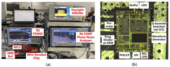
Figure 5.
(a) Measurement setup environment for the f0 output spectrum (with Keysight N9030A), chirp signal analyzing (with R&S FSW85), and phase noise (with R&S FSWP Phase Noise Analyzer) of the K-band FMCW source chip; (b) photograph of the wire-bonded K-band FMCW source chip.
Figure 6a shows the measured output frequency range of the K-band Q-boosted switched inductor VCO, which is from 24.738 to 26.447 GHz for switch OFF-state (Vsw = 0 V), and 25.438 to 27.566 GHz for switch ON-state (Vsw = 1.2 V). Both are 0.04~0.1 GHz lower than the simulated results, possibly due to the parasitics from the circuit layout and active model inaccuracies. If followed by a frequency tripler, the VCO can cover 76~77 GHz (for LRR application) when the varactor tuning voltage, Vt, is at 0.68~1.18 V for switch OFF-state, and 77~81 GHz (for SRR application) when Vt is at 0.21~1.59 V for switch ON-state. At these tuning voltage ranges, the CP has well-matched up/down currents, which helps to optimize the phase noise and spur performance for the proposed FMCW frequency synthesizer. Meanwhile, the average VCO gain, Kvco, is approximately 0.76 GHz/V for Vsw = 0, and 1.02 GHz/V for Vsw = 1.2 V. The lower Kvco value at Vsw = 0 will also improve the phase noise for LRR applications.
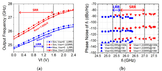
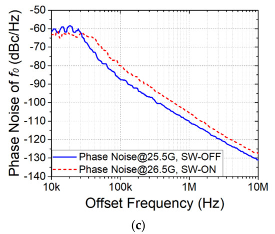
Figure 6.
(a) Measured and simulated output frequency range for the K-band Colpitts VCO using Q-boosted switched inductor at switch ON/OFF states, and short-range radar (SRR)/long-range radar (LRR) frequency range if using a frequency tripler; (b) measured phase noise performance of the Q-boosted switched inductor VCO at switch OFF (for LRR)/ON (for SRR); (c) measured phase noise of the K-band FMCW frequency synthesizer at 25.5 GHz (switch-OFF, blue line), and at 26.5 GHz (switch-ON, red line).
Figure 6b shows the measured Q-boosted switched inductor VCO phase noise from 100 kHz to 10 MHz offset at switch OFF/ON states. VCO shows best phase noise (blue dots) at switch OFF state (Vsw = 0 V), with −115 dBc/Hz@1 MHz, which is desirable for LRR applications. At switch ON-state (Vsw = 1.2 V), the phase noise (red dots) is −110.7 dBc/Hz@1 MHz. Thanks to the Q-boosted switched inductor technique, the VCO phase noise at switch ON-state can be improved by 3~4 dB, compared to the conventional switched inductor VCO [8]. Figure 6c shows the measured phase noise of the K-band FMCW frequency synthesizer, which is −110.5 dBc/Hz@1 MHz at 25.5 GHz (switch OFF-state, blue line), and −106 dBc/Hz@1MHz at 26.5 GHz (switch ON-state, red line), respectively. The loop bandwidth of the synthesizer is designed as ~30 kHz. Compared to the stand-alone Q-boosted switch inductor VCO, the out-of-band phase noise of FMCW frequency synthesizer degenerated by 4~5 dB at 1 MHz offset, which is probably due to the noise coupling from the chip substrate and on-chip power supply.
Figure 7a shows the measured output spectrum for the FMCW source when the VCO inductor switch is at OFF-state. The output spectrum has been converted to 3f0 frequency, based on the K-band f0 chirp from 25.3~25.7 GHz. Figure 7b clearly shows a modulated triangular shape consisting of repeated up and down chirps with bandwidth of 1.2 GHz and duration of 82 μs, which gives the chirp rate of ±14.6 MHz/μs. The normalized root mean square (RMS) frequency error is 517.9 kHz, including the joint points between up and down ramps.
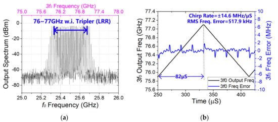
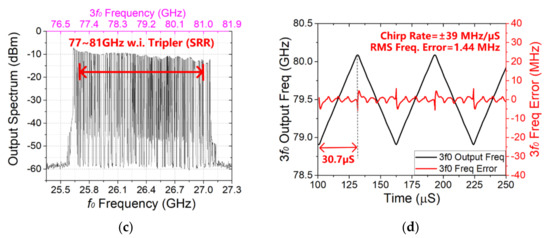
Figure 7.
Measured results for the FMCW source with a triangular chirp: (a) the converted 3f0 output spectrum covering 76~77 GHz when the VCO inductor switch is at OFF-state; (b) the converted 3f0 frequency waveform and frequency error for LRR-band; (c) the converted 3f0 output spectrum covering 77~81 GHz when the VCO inductor switch is at ON-state; (d) the 3f0 frequency waveform and frequency error for SRR-band.
Figure 7c shows the measured output spectrum when the VCO inductor switch is at ON-state. The output spectrum has also been converted to 3f0 frequency, based on the K-band f0 chirp. For SRR application, the chirp rate needs to be high to avoid baseband flicker noise, and chirp bandwidth needs to be wide to permit measurements of reasonably large speeds. Limited by the chirp analyzing bandwidth of the R.S. signal spectrum analyzer FSW85, the measured chirp bandwidth for f0 is set as 400 MHz, or equivalently 1.2 GHz for 3f0 signal. Figure 7d shows a modulated triangular chirp signal with a bandwidth of 1.2 GHz and a duration of 30.7 μs, which gives a chirp rate of ±39 MHz/μs. Meanwhile, the loop bandwidth of the synthesizer has been set as 0.5~1 MHz, in order to lower down the RMS frequency error at high chirp rate. The normalized root mean square (RMS) frequency error is 1.44 MHz.
The proposed FMCW frequency synthesizer is able to generate multi-slope chirps with up to 32 programmable settings for different bandwidths and modulation times. In order to verify this function, triangular-shaped, sawtooth-shaped, and trapezoidal-shaped chirps with different chirp bandwidths and durations are measured, as shown in Figure 8. The triangular-shaped chirp consists of the UP/DOWN modes, the sawtooth-shaped chirp consists of the UP/RST modes, and the trapezoidal-shaped chirp consists of the UP/HOLD/DOWN modes. Each mode of the chirps has a different chirp rate and bandwidth. The three chirp waveforms are programmed for repeated generation after a START code. Comparison of the state-of-the-art FMCW sources for radar applications is listed in Table 1. The proposed FMCW source provides low phase noise, low RMS frequency error, as well as wide frequency range, and high chirp rate. Meanwhile, various chirp shapes can be programmed using the integrated waveform generator.
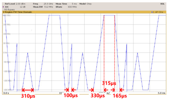
Figure 8.
Measured fundamental frequency waveform of a multi-slope chirp sequence.

Table 1.
Comparison of state-of-the-art FMCW sources for radar applications.
4. Conclusions
In this article, the development of a K-band FMCW frequency synthesizer with an integrated multi-chirp generator is presented. By utilizing Q-boosted switched-inductor VCO, low phase noise, wide chirp bandwidth, steep modulation rates, and high chirp linearity can be obtained for the LRR (76~77 GHz) and SRR (77~81 GHz) applications. An experimental prototype has been designed and fabricated in a 0.13 μm SiGe BiCMOS process. For 77 GHz band, the normalized phase noise is measured as −101 dBc/Hz for switch OFF-state, and −96.5 dBc/Hz for switch ON-state at 1 MHz offset. The normalized root mean square (RMS) frequency error is 518 kHz for chirp rate of ±14.6 MHz/μs and 1.44 MHz for chirp rate of ±39 MHz/μs. Moreover, the integrated waveform generator offers complete programmability in chirp rate, duration and bandwidth, which supports multi-slope chirp generations. With a frequency tripler, the proposed K-band FMCW frequency synthesizer is well suited for the 76~81 GHz FMCW radar system.
Author Contributions
Conceptualization, Z.C.; formal analysis, Z.C., and D.H.; circuit design, Z.C., L.B., and Z.H.; validation, J.-X.C., P.Y., Y.Z.; review and editing, Z.C. and J.-X.C. All authors read and agreed to the published version of the manuscript.
Funding
This research was supported by MISIC Microelectronics.
Conflicts of Interest
The authors declare no conflict of interest.
References
- Schneider, M. Automotive radar—Status and trends. In Proceedings of the German Microwave Conference, Munich, Germany, 16–18 March 2005; pp. 144–147. [Google Scholar]
- Hasch, J.; Topak, E.; Schnabel, R.; Zwick, T.; Weigel, R.; Waldschmidt, C. Millimeter-wave technology for automotive radar sensors in the 77 GHz. IEEE Trans. Microw. Theory Tech. 2012, 60, 845–860. [Google Scholar] [CrossRef]
- Park, J.; Ryu, H.; Ha, K.-W.; Kim, J.-G.; Baek, D. 76-81-GHz CMOS transmitter with a phase-locked-loop based multichirp modulator for automotive radar. IEEE Trans. Microw. Theory Tech. 2015, 63, 1399–1408. [Google Scholar] [CrossRef]
- Rezaei, M.; Aghdam, K.M. Phase Noise Reduction in Low Cost 24/77 GHz FMCW Sensors. In Proceedings of the 2018 18th Mediterranean Microwave Symposium (MMS), Istanbul, Turkey, 31 October–2 November 2018; pp. 229–232. [Google Scholar]
- Milosavljevic, I.M.; Glavonjic, D.P.; Krcum, D.P.; Jovanovic, S.P.; Mihajlovic, V.R.; Milovanovic, V.M. A 55–64-GHz Fully Integrated Miniaturized FMCW Radar Sensor Module for Short-Range Applications. IEEE Microw. Wirel. Compon. Lett. 2019, 29, 677–679. [Google Scholar] [CrossRef]
- Bayram, E.; Hanay, O.; Negra, R. Low-power multiband hybrid VCO for 77/81 GHz FMCW long range radar applications. In Proceedings of the 2018 11th German Microwave Conference (GeMiC), Freiburg, Germany, 12–14 March 2018; pp. 55–58. [Google Scholar]
- Ergintav, A.; Herzel, F.; Fischer, G.; Kissinger, D. Multiplexed Twin PLLs for Wide-Band FMCW Chirp Generation in 130-nm BiCMOS. IEEE Microw. Wirel. Compon. Lett. 2019, 29, 483–485. [Google Scholar] [CrossRef]
- Song, J.H.; Cui, C.; Kim, S.K.; Kim, B.S.; Nam, S. A Low-Phase-Noise 77-GHz FMCW Radar Transmitter With a 12.8-GHz PLL and a ×6 Frequency Multiplier. IEEE Microw. Wirel. Compon. Lett. 2016, 26, 540–542. [Google Scholar] [CrossRef]
- Chen, Z.; Chen, J.X.; Yan, P.P.; Hou, D.B.; Zhu, F. K-Band Low Phase Noise VCO Based on Q-Boosted Switched Inductor. Electronics 2019, 8, 1132. [Google Scholar] [CrossRef]
- Chen, Z.; Wang, M.; Chen, J.X.; Liang, W.F.; Yan, P.P.; Zhai, J.F.; Hong, W. Linear CMOS LC-VCO Based on Triple-Coupled Inductors and Its Application to 40-GHz Phase-Locked Loop. IEEE Trans. Microw. Theory Tech. 2017, 65, 2977–2989. [Google Scholar] [CrossRef]
- Evren, C.; Ferdi, T.; Onur, D.; Lutfiye, D. Multi-user shared access in massive machine-type communication systems via superimposed waveforms. Phys. Commun. 2019, 37, 100896. [Google Scholar]
- Wang, B.; Gao, H.; Dommele, A.R.; Matters-Kammerer, M.K.; Baltus, P.G.M. 60-GHz Low-Noise VGA and Interpolation-Based Gain Cell in a 40-nm CMOS Technology. IEEE Trans. Microw. Theory Tech. 2019, 67, 518–532. [Google Scholar] [CrossRef]
- Gao, H.; Matters-Kammerer, M.K.; Baltus, P.G.M. A 60 GHz Low Power Self-mixing Receiver in 65-nm CMOS for a Radio-Triggered Battery-Less Monolithic Wireless Sensor. IEEE J. Emerg. Sel. Top. Circuits Syst. 2018, 8, 240–250. [Google Scholar] [CrossRef]
- Long, J.R. On-chip transformer design and application to RF and mm-wave front-ends. In Proceedings of the 2017 IEEE Custom Integrated Circuits Conference (CICC), Austin, TX, USA, 30 April–3 May 2017; pp. 1–43. [Google Scholar]
- Lee, T.H. The Design of CMOS Radio-Frequency Integrated Circuits, 2nd ed.; Cambridge University Press: Cambridge, UK, 2004. [Google Scholar]
- El-Shennawy, M.; Joram, N.; Ellinger, F. Fractional-N PLL optimization for highly linear wideband chirp generation for FMCW radars. In Proceedings of the 2015 German Microwave Conference (GeMiC), Nuremberg, Germany, 16–18 March 2015; pp. 248–251. [Google Scholar]
Publisher’s Note: MDPI stays neutral with regard to jurisdictional claims in published maps and institutional affiliations. |
© 2020 by the authors. Licensee MDPI, Basel, Switzerland. This article is an open access article distributed under the terms and conditions of the Creative Commons Attribution (CC BY) license (http://creativecommons.org/licenses/by/4.0/).