Article

A Negative Charge Pump Using Enhanced Pumping Clock for Low-Voltage DRAM

School of Electrical and Electronic Engineering, Yonsei University, Seoul 03722, Korea
*
Author to whom correspondence should be addressed.
Electronics 2020, 9(11), 1769; https://doi.org/10.3390/electronics9111769
Submission received: 30 September 2020 / Revised: 21 October 2020 / Accepted: 23 October 2020 / Published: 26 October 2020
(This article belongs to the Special Issue Low-Voltage Integrated Circuits Design and Application)

Abstract

:
As the supply voltage decreases, there is a need for a high-speed negative charge pump circuit, for example, to produce the back-bias voltage (VBB) with high pumping efficiency at a low supply voltage (VDD). Beyond the basic negative charge pump circuit with the small area overhead, advanced schemes such as hybrid pump circuit (HCP) and cross-coupled hybrid pump circuits (CHPC) were introduced to improve the pumping efficiency and pump down speed. However, they still suffer from pumping efficiency degradation, low level |VBB|, and small pumping currents at very low VDD. A novel negative charge pump using an enhanced pumping clock is proposed. The proposed cross-coupled charge pump consists of the enhanced pumping clock generator (ECG) having a pair of inverters and PMOS latch circuit to produce an enhanced control signal with a greater amplitude, thereby working efficiently especially at low supply voltages. The proposed scheme is validated with a HSPICE simulation using the TSMC 180 nm process. The proposed scheme can be operated down to VDD = 0.4 V, and |VBB|/VDD is obtained to be 86.1% at VDD = 0.5 V and Cload = 20 nF. Compared to the state-of-the-art CHPC scheme, the pumping efficiency is larger by 35% at VDD = 0.6 V and RL = 10 KΩ, and the pumping current is 2.17 times greater at VDD = 1.2 V and VBB = 0 V, making the circuit suitable for very low supply voltage applications in DRAMs.

1. Introduction

The need for low-power circuits has drastically increased with the wide spread of mobile applications and wearable devices. The supply voltage is lowered for low power operation, but the threshold voltage is seldom scaled proportionally due to a sharp leakage current increase [1]. With the high threshold voltage, the leakage current in sub-threshold voltage region is diminished, but the circuit must be content with a degraded operation speed. Therefore, a multi-threshold system [1] employs the low threshold voltage transistors in selective parts where the fast operating speed is required and the high threshold voltage transistors elsewhere. On the other hand, for the variable threshold voltage schemes [2,3], the threshold voltage of MOS transistors is changed with the controlled voltage between the bulk and source nodes. Using the substrate bias circuit, the threshold voltage can be decreased to increase the operation speed during on-states, while the threshold voltage can be increased to reduce the steady power consumption during off-states. In DRAM, the leakage current [4,5,6] in the cell access transistor, aggravated by the scaling in the supply voltage and the storage cell dimensions, reduces the data retention time. As a result, the refresh time must be shortened, and the power consumption is increased. To reduce the leakage current, the method of increasing the threshold voltage with an internal negative voltage generator is truly vital for DRAMs [4,7,8].
The Dickson charge pump [4,9] consisting of diode connected transistor and pumping capacitor is simple but has a low pumping efficiency because the threshold voltage drop in the diode connected transistor hinders charge transfer from the load to ground. To improve the pumping efficiency, a hybrid pumping circuit (HPC) [10] using NMOS and PMOS transistors is introduced. An auxiliary circuit consisting of diode connected PMOS and small capacitor provides the appropriate pumping control signal under the condition that VDD is higher than 2 times the threshold voltage. A cross-coupled hybrid charge pump circuit (CHPC1) [11] is introduced to improve the pump down speed and pumping efficiency at low VDD. This circuit has two pumping branches whose controls are provided by non-overlapping clock signals. CHPC1 increases the pump down speed using sequential pump down operations and mitigates VDD constraints using non-overlapping pumping clocks. In another cross-coupled hybrid charge pump circuit (CHPC2) [7], the pumping nodes are disconnected from the gate nodes in the opposite pumping branch transistors, but the auxiliary circuit is needed to serve as the gate control signal. Both CHCP1 and CHPC2 show better pumping efficiencies and pump down speeds but still have considerable performance degradation at very low VDD. We present a negative charge pump circuit using enhanced pumping clock to serve as a negative voltage generator with a high efficiency and fast pump down speed at very low supply voltage.
In Section 2, conventional negative charge pumps are reviewed. In Section 3, the proposed scheme is presented with performance benefits explained at low supply voltage. Various performance aspects are evaluated for the proposed and conventional schemes in Section 4. Conclusions are drawn in Section 5.

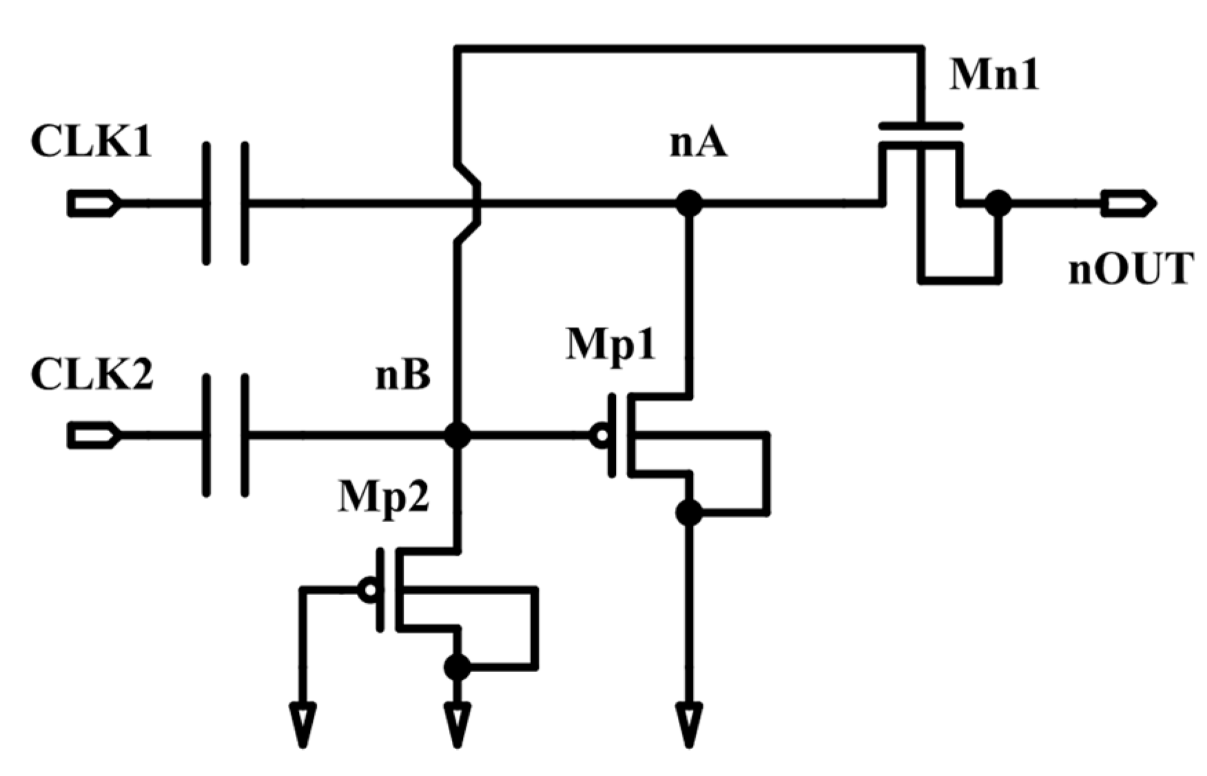
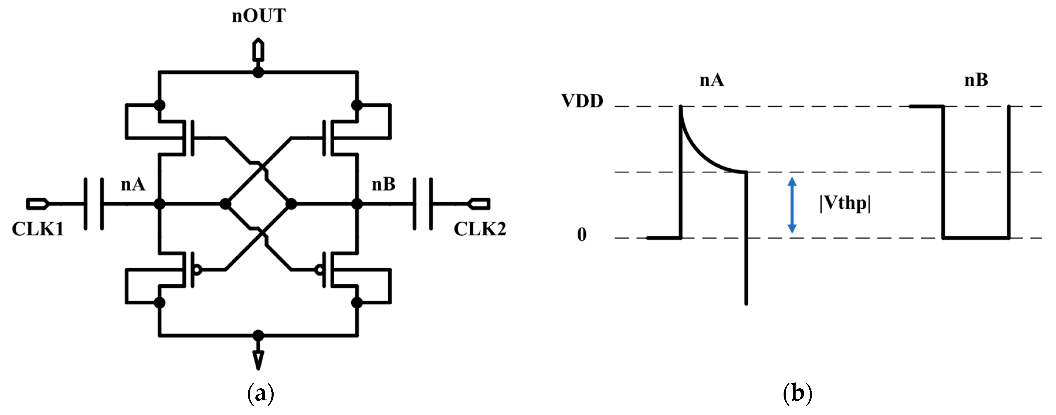
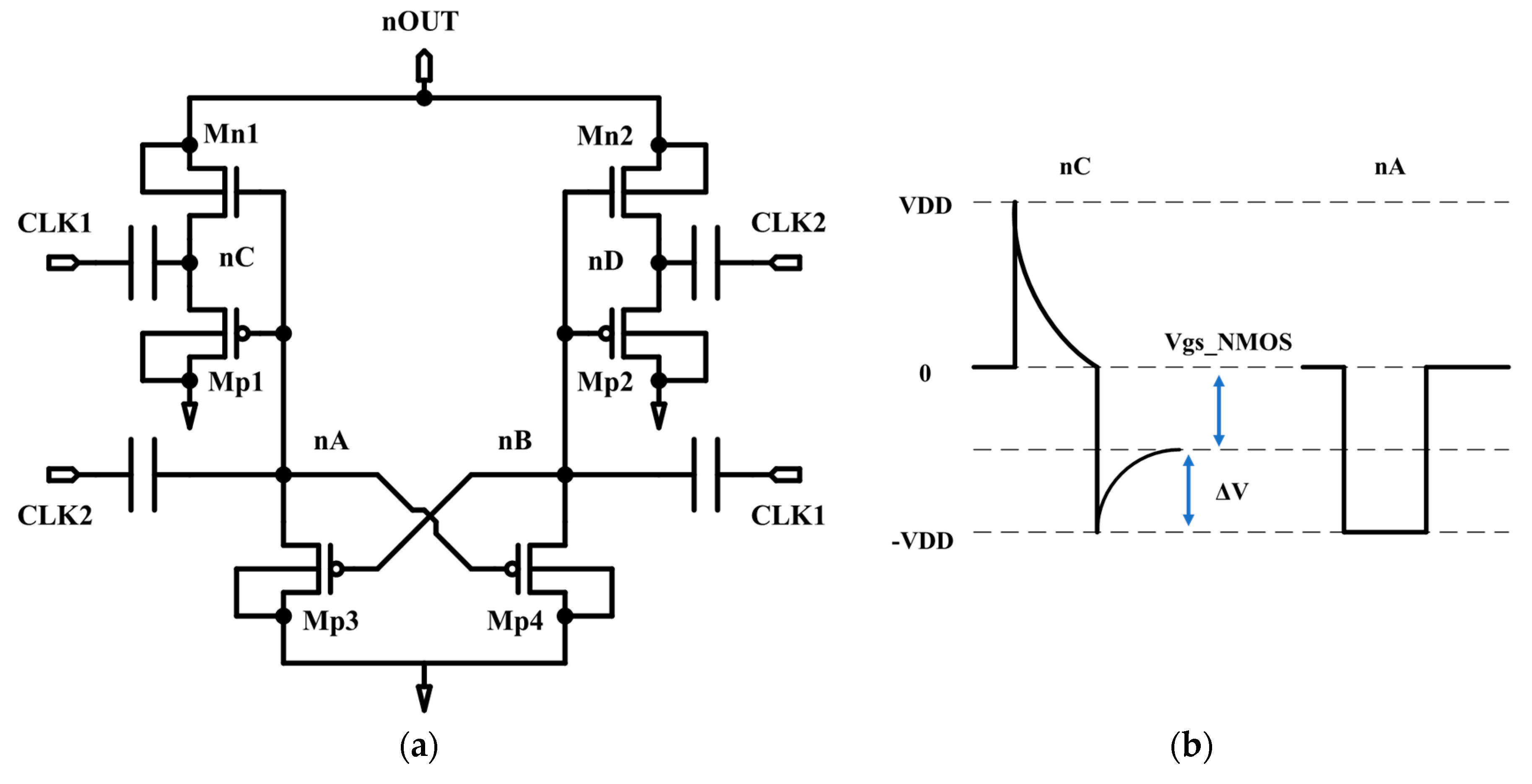
2. Conventional Negative Charge Pump Circuits

Figure 1 shows the schematic diagram of the hybrid pumping circuit (HPC). The HPC scheme consists of transfer transistor (Mn1), discharge transistor (Mp1), and auxiliary transistor (Mp2). The gate nodes of Mn1 and Mp1 are connected together from which Mp2 links to the ground rail in a diode connected configuration [6,10]. The pumping clocks, CLK1 and CLK2, are two non-overlapping clocks. Through diode connected Mp2, nB remains at a positive voltage when CLK2 goes ‘high’. As a result, the charge transfer is facilitated because Mn1 maintains a relatively high gate voltage during the charge transfer operation from nOUT to nA. However, VDD has to be 2 times higher than |Vthp| for proper operation for Mp2. Therefore, HPC is not suitable for very low supply voltage conditions.
Figure 2 shows the schematic diagram of the cross-coupled hybrid pump circuit 1 (CHPC1). A pair of inverters is connected in a cross-coupled configuration [12,13,14]. The pumping capacitors are controlled by non-overlapping clocks. The voltage difference between nA and nB is VDD. If VDD is higher than |Vthp|, PMOS transistors are turned on and off alternately. Because the VDD constraint of CHPC1 is reduced over HPC, CHPC1 is better than HPC in a low voltage condition. There exists a phenomenon of pumping speed degradation at the initial pump down operation.
In CHPC1, the two pumping nodes (nA, nB) are connected to the output node (nOUT) through NMOS latch circuit. During the initial pumping operations, nA and nB do not have sufficiently low voltage values. Therefore, the voltage at the node nA (VnA) remains still positive when CLK1 is ‘high’. When CLK1 goes to ‘low’ and CLK2 goes to ‘high’, charge sharing takes place between nOUT and nA. Because the load capacitance is generally larger than the pumping capacitance, VnA reflects the charge shared voltage from VnOUT. In the next pumping clock, VnB is lowered by CLK2, but Mp1 turns on weakly because VnB is not fully discharged by relatively high VnA. Hence, the pump down speed slows during the initial pumping operation period.
The cross-coupled hybrid pump circuit 2 (CHPC2) is shown in Figure 3. It consists of a pair of HPC and cross-coupled PMOS latch [7,15]. The HPC circuit in the CHPC2 is controlled by the non-overlapping pump clocks, CLK1 and CLK2, respectively, and the gate node of HPC circuit is connected to the output of cross-coupled PMOS latch. The distinguishing difference is that the pumping nodes (nC, nD) are separated from gate nodes (nA, nB). The output nodes of PMOS latch (nA, nB) are operated with auxiliary pump capacitors which are controlled by CLK1 and CLK2. VnA and VnB easily swing from −VDD to 0 because nA and nB are separated from nC and nD, respectively. When CLK1 is ‘high’, VnC is increased and VnA is decreased to −VDD. VnC discharges to the ground through Mp1.
At the next clock phase when CLK1 goes to ‘low’, VnC is decreased and VnA is increased to 0. With the charge sharing through Mn1, VnOUT decreases and VnC increases. With repeated pumping operations, VnOUT can be lowered to −VDD. In the initial pumping operation, CHPC2 can overcome the drawbacks of CHPC1 using independent gate control nodes. Yet, the voltage elevation of nC weakens the charge sharing performance. This weakness is further aggravated with the large load capacitance and small pumping capacitance. To increase the pump down speed and the efficiency at low supply voltage, considerations and measures are required to improve not only the discharge operation but also the transfer operation.

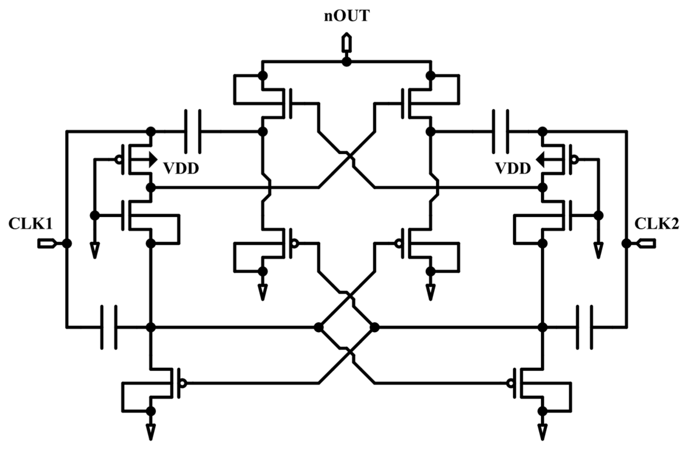
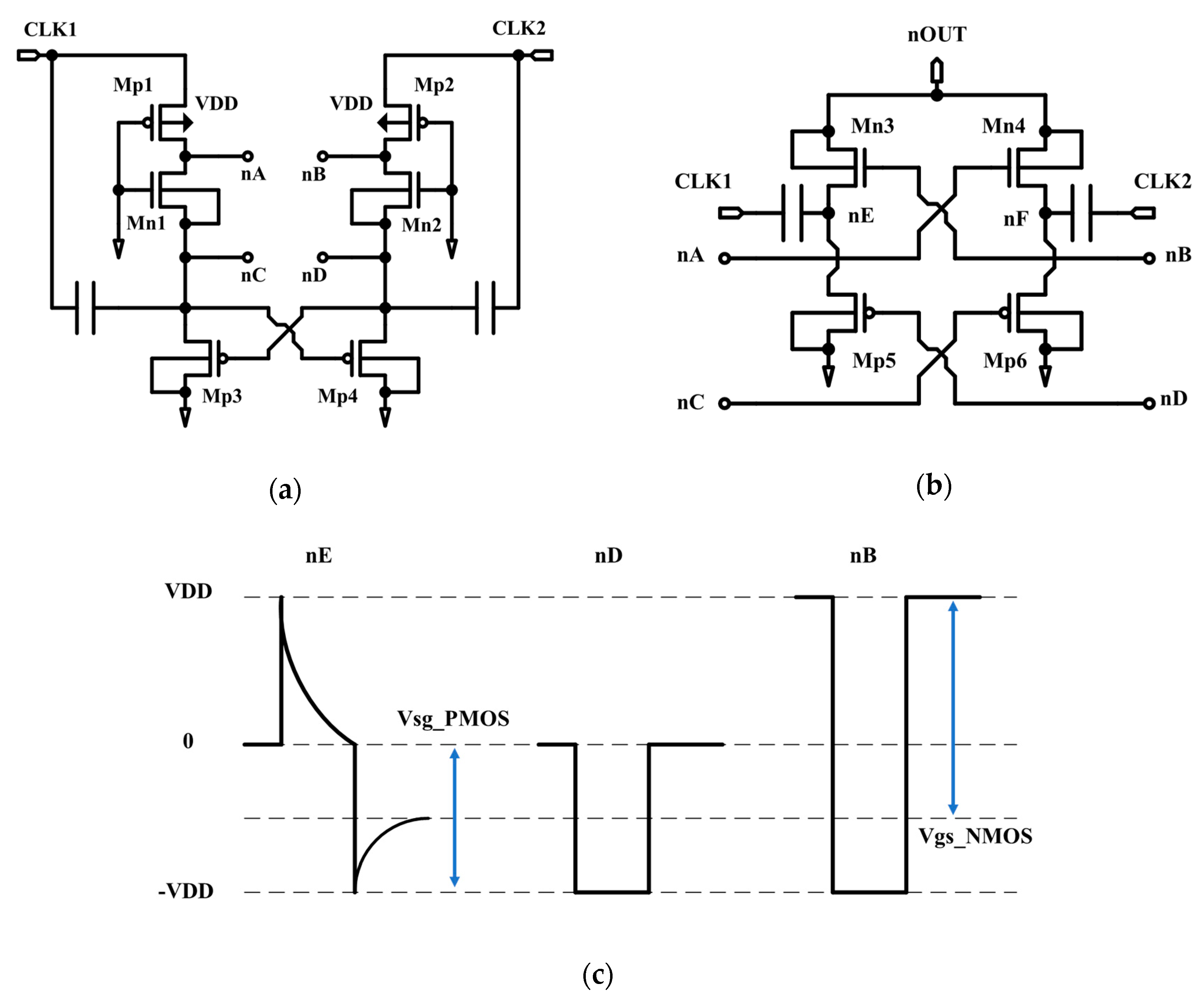
3. Enhanced Clock Pump Circuit (ECPC)

Figure 4 shows the proposed enhanced clock pumping circuit (ECPC). The proposed circuit consists of the enhanced pumping clock generator (ECG) and the cross-coupled pumping circuit (CCP) which are shown in Figure 5a,b, respectively. The ECG circuit consists of a pair of inverters and PMOS latch circuit. The ECG generates the control signal for CCP using non-overlapping clock signals. When CLK1 is ‘high’ and CLK2 is ‘low’, the PMOS transistor, Mp1, is turned on, and VnA rises to VDD. On the other hand, the node nC is discharged to the ground because VnD is decreased by CLK2 after the PMOS transistor, Mp3, is turned on. Therefore, the NMOS transistor, Mn1, is turned off, and nA is isolated from nC. On the other side, the transistors, Mp2 and Mp4, are turned off, and VnD is decreased to −VDD. Therefore, Mn2 is turned on and VnB turns to −VDD. So, the voltages on nA, nB, nC, and nD become VDD, −VDD, 0, and −VDD, respectively. It can be seen that ECG generates two types of non-overlapping control signals. The voltages of nA and nB swing from −VDD to VDD, and the voltages of nC and nD swing from −VDD to 0. The CCP circuit consists of a pair of NMOS transfer transistors and a pair of PMOS discharge transistors. The gate nodes of transfer transistors, Mn3 and Mn4, are connected to nB and nA, respectively. The gate node discharge transistors, Mp5 and Mp6, are controlled by nodes nC and nD, respectively. When CLK1 is ‘high’, VnA is VDD, VnB is −VDD, VnC is 0, and VnD is −VDD. When CLK1 rises, nE is increased, and charges stored in the pumping capacitor are discharged through Mp5. As a result, VnE is lowered to 0. Next, CLK1 goes to ‘low’ and CLK2 goes to ‘high’. VnA, VnB, VnC, and VnD become −VDD, VDD, −VDD, and 0, respectively. Then, the charge sharing occurs through Mn3. Because VnB is sufficiently high, the charge sharing operation between nE and nOUT takes place without voltage loss incurred by the threshold voltage drop, achieving a high pumping speed. In the next clock phase, the analogous pump down operation is performed in the opposite pumping branch. Using the ECG circuit, transfer transistors of CCP are provided with sufficiently high voltage to serve an effective charge transfer from the load capacitor even during the early pumping period.
Besides, the discharge operation is efficiently performed as well by the ECG circuit for being enabled with the low voltage to discharge transistor of CCP.

4. Simulation Results

To evaluate the performance of the proposed ECPC scheme, a HSPICE simulation with the TSMC 180 nm process is performed. The threshold voltages of NMOS and PMOS with no body bias are 0.445 V and −0.437 V, respectively, with the body bias range being 0.430 V–0.474 V and −0.464 V–−0.437 V. The surface mobilities for the NMOS and PMOS transistors are 0.0459 m2/V-s and 0.0109 m2/V-s, respectively. The channel doping concentrations for NMOS and PMOS transistors are 3.90 × 1017 cm−3. The width ratio between the transfer transistor and the discharge transistor is chosen to be 1/2 for all the circuits in the comparison. The auxiliary PMOS transistor in the HPC is sized at 1/10th the width of the discharge transistor. The auxiliary PMOS latch in the CHPC2 is also sized at 1/10th the width of the discharge transistor. In the proposed scheme, the widths of PMOS and NMOS in ECG circuit are sized at 1/10th the widths of its discharge and transfer transistors, respectively. The load capacitance (CLOAD) is 20 nF, the pumping capacitance (CPUMP) is 1 nF, the auxiliary pumping capacitance in HPC, CHPC2, and ECPC are all 0.1 nF, and the pumping clock frequency is 10 MHz. Performance parameters such as the pump down speed, the |VBB|/VDD ratio, the pumping current, and the pumping efficiency are analyzed in comparison with the conventional schemes. For brevity, HPC, CHPC1, and CHPC2 are to be denoted as Conv 1, Conv 2, and Conv 3, respectively.

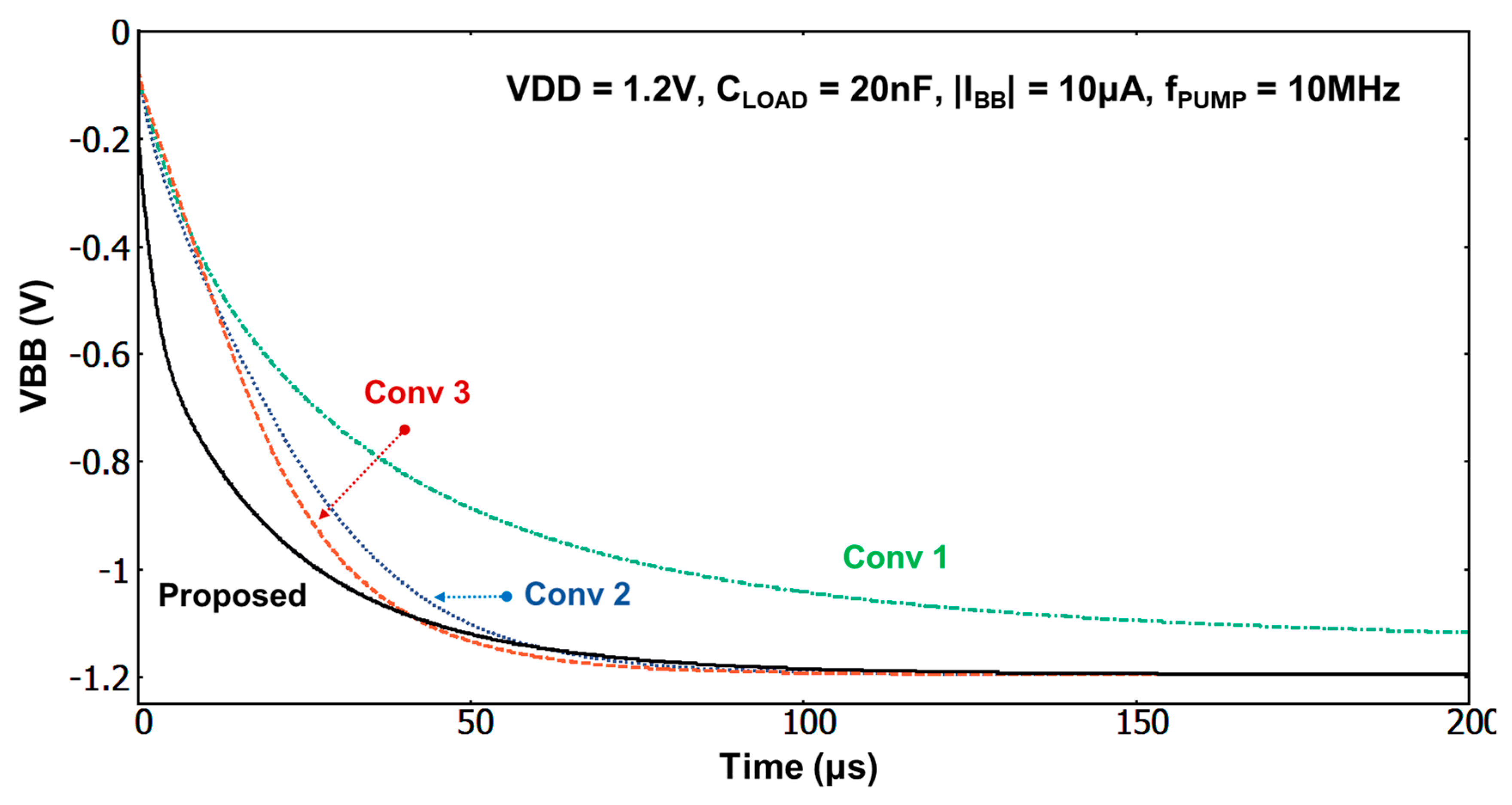
4.1. Pump down Speed

Figure 6 shows the time-traced pump down speeds. Since the bulk bias of the transfer transistors is connected to the VBB node, the threshold voltage of transfer transistors is relatively high at the early operation phase. The drain current of the transfer transistors is proportional to the carrier mobilities and Vgs − Vth. The negative bulk voltage increases the threshold voltage and reduces the carrier mobilities. As a result, the drain currents of transfer transistor are degraded, then the pump down speed slows down. As |VBB| approaches VDD, the pump down speed slows down because the value of Vgs − Vth is decreased, resulting in reduced pumping currents. Therefore, a trade-off issue between the pump down speed and the |VBB| level exists. The single-branched structure of Conv 1 inevitably leads to the worst pump down speed. And the charges at pumping nodes cannot be fully discharged because the source-gate voltage difference for the auxiliary PMOS transistor is not sufficient. Therefore, Conv 1’s |VBB| achieves 93% of VDD with the slowest pump down speed. In Conv 3, the pumping nodes are separated with gate nodes. Using the auxiliary PMOS latch and an additional pumping capacitor, appropriate gate control signals are provided to each pumping branch. As such, the pump down speed of Conv 3 is faster than that of Conv 2. Our proposed scheme shows the fastest pump down speed among all. The ECG circuit of the proposed scheme generates sufficiently high voltage to control the transfer NMOS transistors. This is helpful to overcome the lowered pumping current with increased threshold voltage due to the body bias effect.

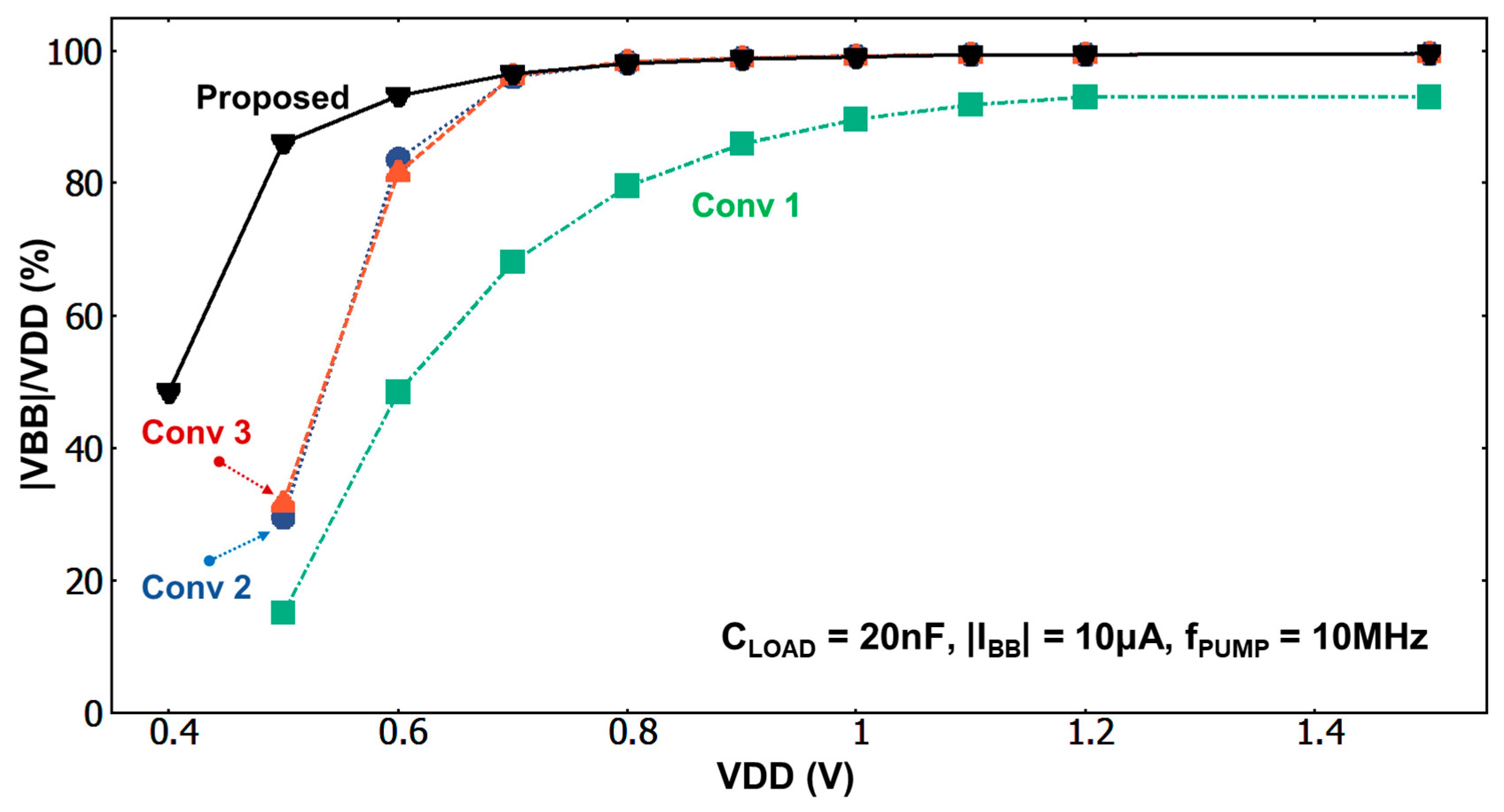
4.2. |VBB|/VDD Ratio

Figure 7 shows the comparison of the |VBB|/VDD ratios with various supply voltages. The Conv 1 shows the most drastic degradation in the |VBB|/VDD ratio as the supply voltage is lowered. This is due to the fact that the supply voltage which is greater than 2 times the threshold voltage is required to control the discharge PMOS transistors. Conv 2 and Conv 3 both show similarly degraded trend in the |VBB|/VDD ratio. For the supply voltage over 1.0 V, |VBB|/VDD ratio is close to 99%. However, under 0.8 V, they both start to decrease and do not operate properly below 0.5 V. In the low supply voltage condition, the NMOS transfer transistor’s operation is important to effectuate the charge sharing voltage between pumping node and output node down to pump-down voltage of VBB. Yet, Conv 2 and Conv 3 do not have any means to facilitate NMOS transfer transistor’s operation. Conv 3 has the auxiliary circuit to help discharge PMOS transistor but the NMOS transfer transistor is deficient in very low supply voltage.

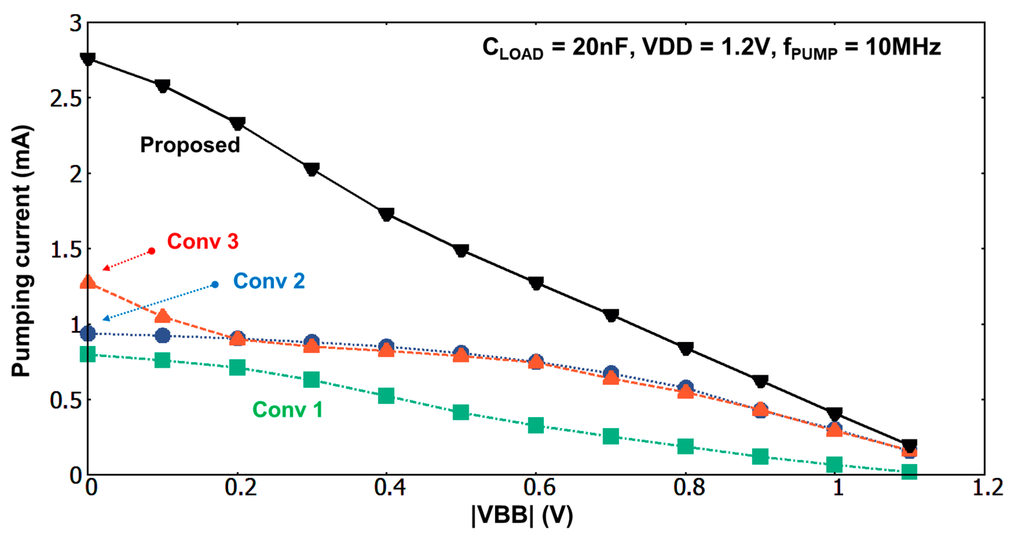
4.3. Pumping Current Comparison with Various VBB

Figure 8 shows the pumping current as a function of VBB at VDD = 1.2 V. As the output voltage approaches the steady value in VBB, the pumping current is decreased because Vds for the NMOS transfer transistor is decreased. Over the entire VBB range, the pumping current of the proposed scheme is larger than all other conventional schemes. This is due to the fact that the ECG circuit generates the large control signal for NMOS transfer transistors. Therefore, the proposed scheme retains relatively high pumping current with high Vgs for the NMOS transfer transistors. For VBB = 0 V, the pumping current of Conv 3 is larger than Conv 2, also in account of its larger pump down speed. The difference in pumping currents between the proposed scheme and other conventional schemes becomes apparent for the low supply voltage. For VBB = 0, the pumping current of Conv 3 is 46% of the proposed scheme at VDD = 1.2 V.
The proposed scheme has the ECG circuit to complement the low voltage operation. As a result, the proposed scheme shows the |VBB|/VDD ratios of 86% and 48% for VDD = 0.5 V and VDD = 0.4 V, respectively. Furthermore, the pumping current of Conv 3 is 19% of the proposed scheme at VDD = 0.6 V. This shows that the proposed scheme will be very suitable for the low supply voltage applications.

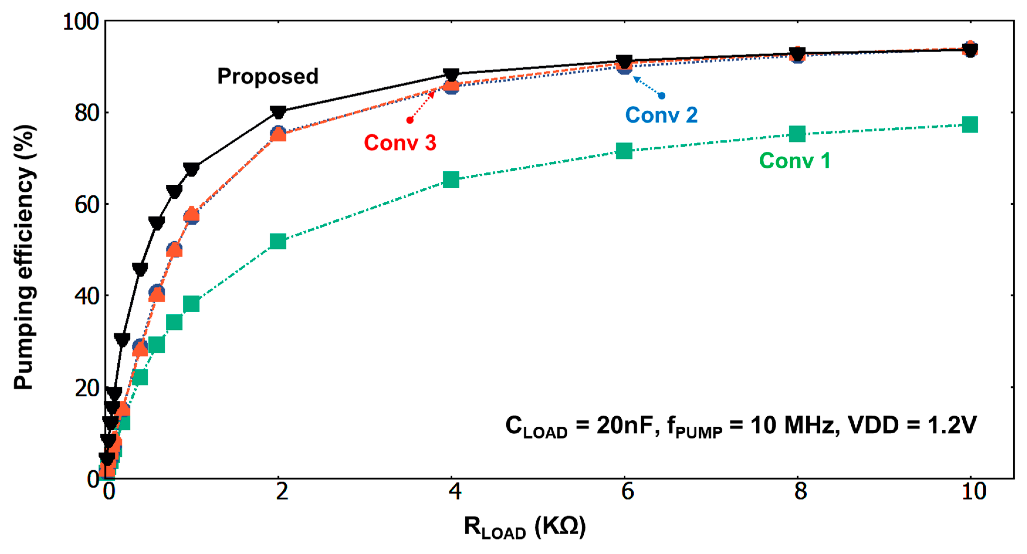
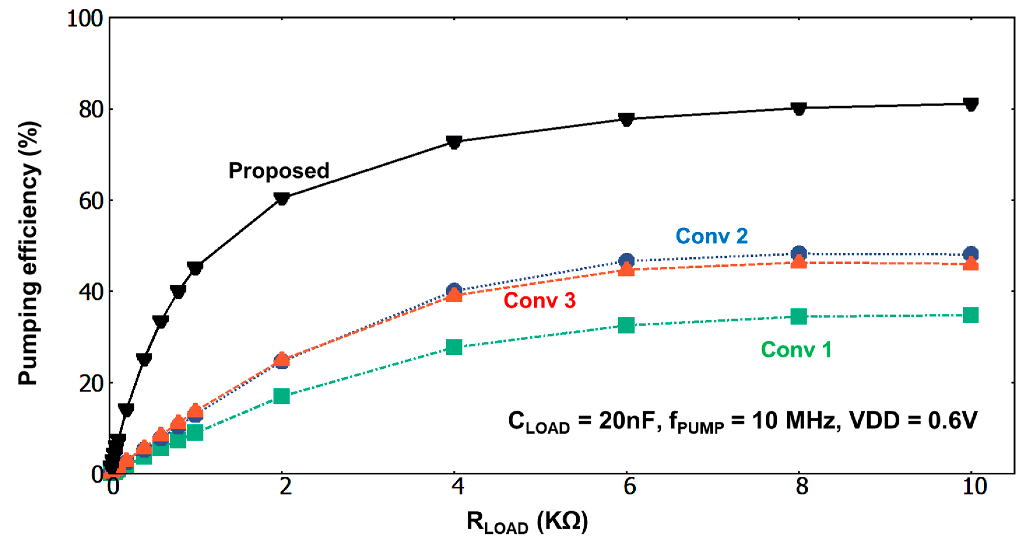
4.4. Pumping Efficiency with Various RLOAD

Figure 9 displays the pumping efficiency with the various load resistance. The pumping efficiency (η) is defined as follows [16]:
η = V BB 2 R LOAD V DD I supply .
As the load resistance decreases, |VBB| is decreased because of the high load current components. The pumping efficiency of Conv 1 is 77.2% with RLOAD = 10 kΩ at VDD = 1.2 V, while all the other schemes achieve pumping efficiencies above 93%. With RLOAD = 1 kΩ, the efficiency of the proposed scheme is 67.6% which is the highest among all. As the supply voltage decreases, the pumping efficiencies drop clearly.
Figure 10 shows the pumping efficiency at VDD = 0.6V. With VDD = 0.6 V and RLOAD = 10 kΩ, the efficiencies of Conv 1, Conv 2, Conv 3, and the proposed scheme are 34.7%, 48.1%, 46.0%, and 81.1%, respectively. The proposed scheme can generate high |VBB| and high pumping current at low supply voltages. The high pumping efficiency shows that the proposed scheme is suitable for low voltage applications.

4.5. Power Loss Estimation

In the topological point view of [17] Conv 1 is bootstrapped, Conv 2 is cross-coupled, Conv 3 is cross-coupled with gate biasing, and the proposed scheme is cross-coupled with clock boosting. In the power loss point of view, two types should be considered. One is the conduction power loss influenced by the resistive condition. The other is the dynamic power loss that depends on the pumping clock frequency and transistor’s capacitive elements [18]. The conduction and the dynamic power losses can be described as:
P C L W I L 2 μ C ox ( V GS V T )
and   P D W I L
where μ is the surface mobility and Cox is the unit area capacitance of the gate oxide. Therefore, the conduction power loss is proportional to the pumping current and inversely proportional to the mobility. The dynamic power loss is proportional to the pumping current and frequency. Conv 1 is assessed with smallest conduction and dynamic power losses due to the smallest transfer transistor size and smallest pumping current. Besides, the auxiliary transistor in Conv 1 for the bootstrap operation is small as well. Conv 2 is next in the order. Conv 2 does not have an auxiliary circuit, but the pumping frequency is greater than Conv 1. As a result, the dynamic power loss for Conv 2 is larger than that for Conv 1. Conv 3 has additional circuit compared with Conv 2. The dynamic power loss in the auxiliary circuit is added. Hence, the power loss of the Conv 3 estimates to be larger than Conv 2. The power loss of the proposed scheme is the largest among all. Because the ECG consumes dynamic power to generate the enhanced clock, the power loss is increased. Together with the largest pumping current, the power loss increases for the proposed scheme.

5. Discussion

For the conventional schemes, the performance of PMOS discharge transistors is improved to increase the pump down speed and pumping efficiency. In this work, the gate voltage of the PMOS discharge transistors can be controlled appropriately in order to increase the initial operating speed and obtain a lower level of VBB. However, as the supply voltage is reduced, the operation of the NMOS transfer transistor is important to maintain the negative charge pump circuit’s performance. Failure to apply sufficiently high voltages to the gate of the NMOS transfer transistors will slow down the charge sharing operation between the pumping node and the load capacitor, leading to pumping current and efficiency reductions. The ECG circuit in the proposed scheme serves both the high positive voltage to activate the NMOS transfer transistors and the low negative voltage to activate the PMOS discharge transistors. In this manner, the proposed negative charge pump scheme can be operated with the high pump down speed and low VBB voltage even with conditions of very low supply voltage and high load current.
The performance of the proposed scheme is now thoroughly evaluated. Table 1 shows the performance of various negative charge pump circuit at VDD=0.6 V and CL=20 nF. The pump-down speed of the proposed scheme is the fastest because the pump-down operation takes place in half clock cycles by using the cross-coupled topology and the large VGS of the NMOS transfer transistors induces large pumping currents. The |VBB|/VDD ratio of the proposed scheme is the largest, too. The large pumping current and the gate control clock from the ECG circuit provide foreseen benefits for the proposed scheme for the low VDD conditions. The pumping efficiency with various load resistance for the proposed scheme is highest because the pumping efficiency is proportional to |VBB|. However, the proposed scheme requires auxiliary transistor and capacitors in forming the ECG circuit. So, the area overhead is largest among them. Besides, the power loss of the proposed scheme is considerable because the ECG circuit continues switching operation that consumes power. Furthermore, the largest pumping current of the proposed scheme increases the dynamic power loss, too, albeit efficiently.

6. Conclusions

A highly efficient and high-speed negative charge pump circuit using enhanced pumping clock generator (ECG) and cross-coupled pumping (CCP) circuit is presented. The ECG supplies the improved control signals to the CCP to enhance its performance. The proposed charge pump circuit shows a comparably fast pump down speed and the |VBB|/VDD ratio which is larger than 93% in the VDD range of 0.6 V–1.5 V. The pumping efficiency of the proposed scheme is higher than 80% with the load resistance in the range of 2 kΩ–10 kΩ at VDD = 1.2 V. Moreover, the pumping current is 2.17 times greater than Conv 3 at VDD = 1.2 V and VBB = 0 V. In very low supply voltage condition of VDD = 0.4 V, the proposed scheme can outperform with the |VBB|/VDD ratio of 48.38%. At VDD = 0.6 V and RLOAD = 10 KΩ, the pumping efficiency of the proposed scheme is 35% larger than Conv 3.

Author Contributions

Conceptualization: C.L.; original draft preparation: C.L.; writing: C.L. and T.Y.; review and editing: C.L. and H.Y.; formal analysis: all authors; supervision: H.Y. All authors have read and agreed to the published version of the manuscript.

Funding

This work was supported by the Technology Innovation Program (10080722, Integrated Server on Chip System Research for Cloud Computing) funded By the Ministry of Trade, industry & Energy (MI, Korea).

Acknowledgments

This work was in part supported by Samsung Electronics, and the EDA tools were supported by the IC Design Education Center (IDEC).

Conflicts of Interest

The authors declare no conflict of interest.

References

  1. Takashima, D.; Watanabe, S.; Nakano, H.; Oowaki, Y.; Ohuchi, K.; Tango, H. Standby/active mode logic for sub-1-V operating ULSI memory. IEEE J. Solid-State Circuits 1994, 29, 441–447. [Google Scholar] [CrossRef]
  2. Kuroda, T.; Fujita, T.; Mita, S.; Nagamatsu, T.; Yoshioka, S.; Suzuki, K.; Sano, F.; Norishima, M.; Murota, M.; Kako, M.; et al. A 0.9-V, 150-MHz, 10-mW, 4 mm2, 2-D discrete cosine transform core processor with variable threshold-voltage (VT) scheme. IEEE J. Solid-State Circuits 1996, 31, 1770–1779. [Google Scholar] [CrossRef]
  3. Srivastava, A.; Zhang, C. An adaptive body-bias generator for low voltage CMOS VLSI circuits. Int. J. Distrib. Sens. Netw. 2008, 4, 213–222. [Google Scholar] [CrossRef]
  4. Martino, W.L.; Moench, J.D.; Bormann, A.R.; Tesch, R.C. An on-chip back-bias generator for MOS dynamic memory. IEEE J. Solid-State Circuits 1980, 15, 820–826. [Google Scholar] [CrossRef]
  5. Seung-Wuk, K.; Seung-Hoon, L.; Jong-Du, J.; Bong-Gyun, K.; Byung-Geun, S.; Jae-Geun, P.; Kae-Dal, K. A novel substrate-bias generator for low-power and high-speed DRAMs. In Proceedings of the IEEE Region 10 Conference. TENCON 99. ‘Multimedia Technology for Asia-Pacific Information Infrastructure’ (Cat. No.99CH37030), Cheju Island, Korea, 15–17 September 1999; Volume 862, pp. 864–867. [Google Scholar]
  6. Kim, Y.H.; Park, H.J.; Sohn, J.D.; Choi, J.S.; Park, C.S.; Ahn, S.H.; Jeong, J.Y. Two-phase back-bias generator for low-voltage gigabit DRAMs. Electron. Lett. 1998, 34, 1831–1833. [Google Scholar] [CrossRef]
  7. Kyeong-Sik, M.; Jin-Yong, C. A fast pump-down VBB generator for sub-1.5-V DRAMs. IEEE J. Solid-State Circuits 2001, 36, 1154–1157. [Google Scholar] [CrossRef]
  8. Shiratake, S. Scaling and performance challenges of future DRAM. In Proceedings of the 2020 IEEE International Memory Workshop (IMW), Dresden, Germany, 17–20 May 2020. [Google Scholar]
  9. Sato, K.; Kawamoto, H.; Yanagisawa, K.; Matsumoto, T.; Shimizu, S.; Hori, R. A 20ns static column 1Mb DRAM in CMOS technology. In Proceedings of the 1985 IEEE International Solid-State Circuits Conference, Digest of Technical Papers, New York, NY, USA, 13–15 February 1985. [Google Scholar]
  10. Tsukikawa, Y.; Kajimoto, T.; Okasaka, Y.; Morooka, Y.; Furutani, K.; Miyamoto, H.; Ozaki, H. An efficient back-bias generator with hybrid pumping circuit for 1.5-V DRAMs. IEEE J. Solid-State Circuits 1994, 29, 534–538. [Google Scholar] [CrossRef]
  11. Cho, C.; Cha, J.; Ahn, M.; Kim, J.J.; Lee, C. Negative charge-pump based antenna switch controller using 0.18 μm SOI CMOS technology. Electron. Lett. 2011, 47, 371–372. [Google Scholar] [CrossRef]
  12. Tan, Y.; Zhan, C.; Wang, G. A fully-on-chip analog low-dropout regulator with negative charge pump for low-voltage applications. IEEE Trans. Circuits Syst. II Express Briefs 2019, 66, 1361–1365. [Google Scholar] [CrossRef]
  13. Justo, D.; Cavalheiro, D.; Moll, F. Body bias generators for ultra low voltage circuits in FDSOI technology. In Proceedings of the 2017 32nd Conference on Design of Circuits and Integrated Systems (DCIS), Barcelona, Spain, 22–24 November 2017; pp. 1–6. [Google Scholar]
  14. Tan, Y.; Zhan, C.; Wang, G. A fully-on-chip low-voltage low-dropout regulator with negative charge pump. In Proceedings of the 2018 IEEE International Conference on Electron Devices and Solid State Circuits (EDSSC), Shenzhen, China, 6–8 June 2018; pp. 1–2. [Google Scholar]
  15. Kyeong-Sik, M.; Kyo-Won, J.; Ji-Beom, K. A high-efficiency back-bias generator with cross-coupled hybrid pumping circuit for sub-1.5 V DRAM applications. In Proceedings of the 26th European Solid-State Circuits Conference, Stockholm, Sweden, 19–21 September 2000; pp. 188–191. [Google Scholar]
  16. Matoušek, D.; Beran, L. Comparison of positive and negative Dickson charge pump and Fibonacci charge pump. In Proceedings of the 2017 International Conference on Applied Electronics (AE), Pilsen, Czech Republic, 5–6 September 2017; pp. 1–4. [Google Scholar]
  17. Ballo, A.; Grasso, A.D.; Palumbo, G. A review of charge pump topologies for the power management of IoT nodes. Electronics 2019, 8, 480. [Google Scholar] [CrossRef] [Green Version]
  18. Chi-Chang, W.; Jiin-Chuan, W. Efficiency improvement in charge pump circuits. IEEE J. Solid-State Circuits 1997, 32, 852–860. [Google Scholar] [CrossRef]
Figure 1. The schematic diagram of hybrid pumping circuit (HPC).
Electronics 09 01769 g001
Figure 2. (a) Cross-coupled hybrid pump circuit 1 (CHPC1) and (b) its voltage waveforms at pumping nodes during the initial pump down operation.
Electronics 09 01769 g002
Figure 3. (a) Cross-coupled hybrid pump circuit 2 (CHPC2) and (b) its voltage waveforms at pumping nodes during the initial pump down operation.
Electronics 09 01769 g003
Figure 4. Proposed enhanced clock pump circuit (ECPC).
Electronics 09 01769 g004
Figure 5. Proposed enhanced clock pump circuit (ECPC) separated into (a) enhanced pumping clock generator (ECG) and (b) cross-coupled pump circuit (CCP) with (c) its voltage waveforms during the initial pump down operation.
Electronics 09 01769 g005
Figure 6. Comparison of the pump down speeds.
Electronics 09 01769 g006
Figure 7. |VBB|/VDD with various supply voltages.
Electronics 09 01769 g007
Figure 8. Pumping current with various VBB.
Electronics 09 01769 g008
Figure 9. Pumping efficiency with various load resistance at VDD = 1.2 V.
Electronics 09 01769 g009
Figure 10. Pumping efficiency with various load resistance at VDD = 0.6 V.
Electronics 09 01769 g010
Table 1. Comparison of various negative charge pump circuits at VDD = 0.6 V and CL = 20 nF.
Conv 1
(HPC)
Conv 2
(CHPC1)
Conv 3
(CHPC2)
Proposed
TopologyBootstrapCross-coupledCross-coupled with gate biasingCross-coupled with clock boosting
|VBB|/VDD ratio 48.5%83.6%81.6%93.2%
Pump-down speed177.8 μs176.4 μs178.7 μs120.0 μs
Pumping current at VBB = 0 V57.7 μA79.9 μA89.8 μA471.6 μA
Pumping efficiency at RL = 10 kΩ34.7%48.1%46.0%81.1%
Publisher’s Note: MDPI stays neutral with regard to jurisdictional claims in published maps and institutional affiliations.

