Abstract
This paper presents a current-based control for a proton-exchange membrane fuel cell using the so-called double dual boost topology. In particular, we introduce a discrete time controller that, in coordination with a particular selection of inductors and capacitors, minimizes the switching ripple at the input port (current ripple) and the output port (voltage ripple) of the double dual boost converter. This converter has a particular characteristic, in contrast to the classical interleaved boost topology, in the double dual boost, the phases of the converter can have different duty ratios. The freedom to choose the duty ration for each phase can be used to select the operative point in which the input current is equal to zero. However, if individual controllers are used for each branch of the converter, the equilibrium after a transient can differ from the minimum ripple operation point; the proposed scheme regulates the output voltage and, at the same time, ensures the equilibrium remains in the minimum ripple operation in steady state. In this way, the converter can mitigate the harmonic distortion on the current extracted from the proton-exchange membrane fuel cell, which is beneficial to improve the efficiency and lifetime of the cell, and on the output voltage delivered to an output direct current bus. The results of the experiment are presented to validate the principles of the proposed system.
1. Introduction
Fuel cells (FCs) and other renewable energy sources are a compelling alternative to conventional pollution-prone power sources [1,2,3,4]. However, there are additional relevant challenges that must be solved to propagate them. For instance, the requirement of voltage or current regulation under wide ranges of operating conditions using power converters. Another important challenge is related to the low amplitude of the output voltage; the output voltage of the fuel cell must be increased and regulated to feed a grid-tie inverter. For instance, the voltage of a traditional fuel cell (FC) stack can be in the order of dozens of volts, while the DC bus voltage requirements for a grid tie inverter are several times higher [1,2]. Furthermore, the input current of some power converters can be a discontinuous signal or a continuous signal with a large switching ripple (variations due to the switching action). This current is drawn from the fuel cell, with a negative impact on the lifetime and performance of fuel cells, as mentioned in several investigations [1,2]. The negative effect of distorted current signals on fuel cells has motivated new investigations [5,6,7,8,9]. It is recommended that the FC current ripple must be lower than 5% to have a good performance. In order to overcome this challenge, new topologies have been designed to operate with lower current ripples than traditional topologies and to provide high voltage gains [3,4].
Several converter topologies can overcome the discussed challenges; for example, quadratic-gain converters ([10,11]) achieve a large voltage gain. The large voltage gain can be used to increase the voltage provided by the fuel cell; the main disadvantage of quadratic converters is the voltage stress across their transistor; this produces a relatively large amount of switching power losses.
Another solution to provide a large voltage gain are multilevel topologies [12,13], which have lower voltage-stress on transistors; on the other hand, multilevel converters contain a significant number of semiconductor devices.
Switched inductor topologies [14,15] and coupled inductors [16,17] have been are also used. Another solution involves switched-capacitor topologies [18,19], which overcome some of those challenges; they feature small size/weight and high power density; however, their best performance and efficiency are obtained in cases in which there is no voltage regulation.
A topology option with large voltage gain and switching ripple cancellation is the one introduced in [20], where it was called the double dual boost converter (DDBC) [20,21,22,23]. In general, it has been shown that the DDBC can achieve input current ripple cancellation and overall satisfactory performance in experimental implementations [20,21,22,23].
This article presents the implementation of a fuel cell generation system. The base of the generation system is a dc–dc converter of a topology called double dual boost converter. The system implementation includes the design of the converter and its experimental validation. The system also includes a closed-loop digital controller. The controller, in coordination with a particular selection of inductors and capacitors, minimizes the switching ripple on the topology, both switching ripples, the input current ripple, and the output voltage ripple. The work includes a hardware-in-the-loop closed-loop implementation, rather than passive based with respect to a fixed operating point, as in the current literature.
This article describes a fully integrated solution to the described challenges. It comprises the hardware in the loop interconnection of two independently controlled systems (the fuel cell emulator and the double dual boost converter). The obtained experimental results involve the design and validation of an FC emulator and a correct selection of passive components (capacitors and inductors) for the converter, along with the controller design in discrete time, which ensures the active minimization of switching ripples. Experimental results are provided to validate the principle of the proposition.
2. Methodology
This article is focused on the dc–dc converter, with particular hardware design and a particular digital controller; the converter is suitable for their use in a fuel-cell based generation system; in order to corroborate their operation, this work started with the design and implementation of a fuel cell emulator based on the hardware in the loop philosophy.
Figure 1 shows the fuel cell emulator, which is based on a controlled dc source, an FPGA-compact Rio 9039 (from National Instruments, Austin, TX, USA) data acquisition system, and a computer with LabView software; the computer program is based on a fuel cell mathematical model which is described on Section 6 of this article. The emulator was built and validated before their connection to the dc–dc double dual boost converter. The power controlled source used for the fuel cell emulator was the Keysight N6953A model (from Keysight Technologies, Santa Rosa, CA, USA).
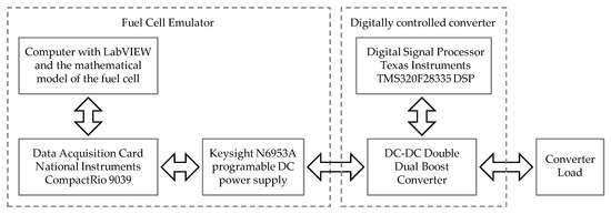
Figure 1.
The full hardware in the loop system developed for this article.
The output of the fuel cell emulator is connected to the double dual boost converter; this particular topology of the converter is described in Section 3 of this article; the experiment was designed in order to validate the implementation of the proposed discrete-time controller under a realistic scenario.
The particular hardware design of the converter is discussed in Section 4 of this article, and the digital control loop is described in Section 5 of this article. The digital controller was implemented on a Texas Instruments TMS320F28335 digital signal processor (From Texas Instruments, Dallas, TX, UAS), see Figure 1.
After the fuel cell emulator was build and tested (some experiments in the experimental results demonstrate their operation), the DDBC was designed, implemented, and tested in open-loop mode. Once the converter operates properly in open-loop mode, a digital controller was designed and tested. To control the converter, the Texas Instruments TMS320F28335 digital signal controller was used.
Finally, the complete system was integrated, and proper operation test was carried out; the two independently controlled systems operated correctly, as shown in the experimental results section, which is Section 7 of this article.
3. The Double Dual Boost Converter (DDBC)
We briefly discuss the main features of the DDBC [20,21,22,23], which is depicted in Figure 2. The DDBC is based on two boost sub-circuits that are connected in input parallel and output series. The difference of this section with most descriptions of the converter in the state of the art is that we are not assuming that both sub-circuits have the same duty; they actually have different duty cycles. The sub-circuit that contains L1, C1, S1, and , is called the upper switching stage, while the lower switching stage contains L2, C2, S2, and .
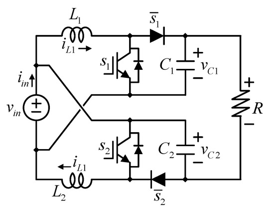
Figure 2.
The topology of a double dual boost converter (DDBC).
For ease of exposition, the converter is assumed to operate in continuous conduction mode. Consequently, when the upper diode is closed, then the upper transistor is open and vice versa; the same consideration applies to the lower switching stage.
The converter operates with the Pulse Width Modulation PWM, which can be explained in the following manner: a defined and constant switching frequency for transistors. The inverse of the switching frequency is the switching period. A duty ratio or duty cycle is the relation among the time a transistor is closed, divided over the total switching period. Figure 3a shows the relevant waveforms when operating with a duty cycle D = 0.7.
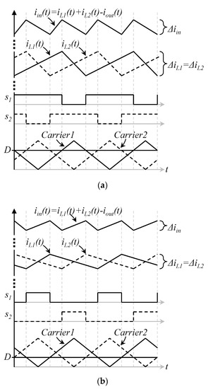
Figure 3.
Relevant waveforms in the DDBC (a) with a duty ratio of 70%, (b) with a duty ratio of 30%.
Figure 3b shows the same waveforms as Figure 3a, but in this case, the duty ratio D = 0.3. The signals S1 and S2 are digital functions, which means they have only two values, 0 or 1, high or low. They are called switching functions because they drive the operation of transistors (1 means the transistor is closed, 0 means the transistor is open). Switching functions are obtained from the comparison of two triangular carriers (Carrier1 and Carrier2) shifted 180° with the duty cycle. The duty cycle seems such a constant value in Figure 3. The relation among the on-time and the switching period can be observed from switching functions, and it can also be expressed as the relation among the constant signal D, divided over the peak value of the triangular carriers.
Both inductors have the same inductance, and the same duty cycle is used for both switching stages. Note that the input current is equal to the sum of the current through both inductors minus the output current. The input current ripple is thus smaller to the sum of inductor currents. In former studies ([20,21,22,23]), transistors are driven by the same duty cycle. However, the converter sub-circuits can have different switching functions without restrictions on the duty cycle.
The input-to-output voltage gain of the DDBC converter is now computed. We use the notation D1 to refer to the duty cycle of the upper switching stage, and D2 is used for that of the lower one. This time there is no restriction for D1 to be equal to D2. The mathematical model of the converter can be obtained with the traditional averaging technique and described as Equations (1)–(4).
On Equations (1)–(4) as well as in Figure 2, vin is the input voltage, L1 and L2, inductors 1 and 2 respectively, C1 and C2 capacitors 1 and 2 respectively, d1 and d2 duty cycles for transistors s1 and s2 respectively, iL1 and iL2 are the currents through inductors L1 and L2, and vC1 and vC2 are the voltages across the capacitors C1 and C2. Finally, iout is the output current of the converter.
Another important equation, which is related to the input current ripple cancelation that will be further explained, is the definition of the input current in terms of the summation of the current through inductors and the output current.
In steady state, considering that voltage in capacitors and current through inductors comply with the small ripple approximation, the average voltage across the inductors. This yields to
The difference from upper case to lower case in all variables, for instead from d1 to D1, indicates the operation regime. The upper case shows the steady-state value, which means no transient or perturbation is present, while the lower case shows the large-signal value, which includes transient behaviors. That is the reason why Equations (1) to (4) are all in lower case, while (6) and (7) are upper case. For example, VC1 represents the steady-state component of vC1.
As a special case in this approach, which leads to the traditional approach, if D1 = D2 = D in (6), then the well-known gain of the double dual boost converter is obtained.
The voltage rating in transistors (the voltage transistors block when they are open) can be expressed as (8).
4. Input Current and Output Voltage Ripple Minimization
Though perfect cancellation of input–current–ripple is a desired characteristic in interleaved converters; it is well-known that this condition is only achievable at specific gains in traditional designs [20,21,22,23]. In contrast with traditional approaches, as mentioned before, in the DDBC, the desired duty cycle can be arbitrarily selected according to the nominal voltage gain, e.g., the case when the duty cycles are linearly dependent; this issue is elaborated in the following: Define D as the base duty cycle for the converter, i.e., D = D1; both D1 and D2, can be expressed as a function of the duty cycle D, as shown in Equation (9).
Duty ratios D1 and D2 take values between 0 and 1, at any time. Equation (6) can be written as Equation (10) after substituting Equation (9).
Being G, the topology voltage gain and k is the constant factor that relates the duty cycle D of the converter to the individual duty cycle of each phase D1 and D2. Equation (10) can be written as Equation (11) after substituting Equation (9):
In order to achieve a total ripple cancellation, there are two conditions that must be satisfied: (i) the current positive derivative of one inductor should be equal to the current negative derivative of the other inductor and vice versa; (ii) the total current ripple of both inductors must have equal magnitude shifted 180°. The second condition can be expressed as:
where ΔiL1 and ΔiL2 are the inductor current ripples, and TS is the switching period of the converter. Using (12) and (9), we can conclude that L2 = kL1. Considering that D1 and D2 are complementary for an operating condition with complete cancellation, this yields:
Note that D* represents the nominal duty cycle at which the current ripple is completely mitigated. D* is constant, D can adopt a value among 0 and 1. The duty ratio in (10) is obtained from (13), for a certain gain G as:
Note that (14) has two solutions. The one associated with a minus before the square root would lead to a different k and D*. If this value is used, the same result is obtained in terms of current ripple cancellation, but the role of the switching stages would be inverted. The designer must consider the power distribution among the different phases of the converter; the designer selects the power rate of the components during the design state. For simplicity, we will follow only one root of (14). Note that k has a minor impact on the gain, which mainly depends on D.
The output voltage switching ripple cancellation is the other crucial characteristic of the converter. Similar to the current ripple cancellation, the current Iout charges the capacitor C1 during the time DTS, and at the same time, the capacitor C2 is being charged with the current equal to IL2 − Iout. Moreover, during the period of time (1 − D)TS, capacitor C2 is discharged by means Iout, and C2 is discharged due to a current equal to IL2 − Iout. To accomplish the output voltage ripple cancellation, we can establish two conditions. (i) The positive voltage derivative in one capacitor must coincide with the negative voltage derivative in the other, and vice versa; (ii) The total voltage ripple of both capacitors must have the same magnitude. The first is satisfied when D = D*. For the second condition, by considering the voltage ripple equation, we have:
From (15), we can conclude that the relationship between C1 and C2 is given by
Then, in order to achieve the simultaneous output voltage ripple and input current ripple cancelation, capacitors must be selected in a way that C2 = kC1, as well as in inductors.
5. Digital Control of the Converter with Switching Ripple Cancelation
This section focusses on the dynamical behavior and the switching ripple cancelation to design a closed-loop controller with the desired characteristics. The dynamic model of the converter is described by (17). The model (17) considers Equations (1) and (2) as well as the constant k that is determined by design using (13) and (16).
where vC1, vC2, iL1, iL2 are the state variables, vin is a non-controller input of the system, which is also a variable, and d is the control input of the system, the variable that we can change to control the output voltage.
From (17), the small-signal linearization technique can be applied to get the small-signal model, which is expressed as:
This model in (18) is expressed in incremental variables, where δIj = IL1 − is the increment of IL1 in reference to the equilibrium reference value IL1, and so on for the other variables. In the following, we consider the discrete-time version of (18), which can be obtained by standard methods. Then, we obtain a state-space linear difference system of the form
where n represents the time; and A and B are constant matrices of dimension 4 × 4 and 4 × 1, respectively.
We aim at guaranteeing the regulation of input current. Hence, a current control-loop is realized with the controller in Equation (20).
where k1, k2 are the controller gains; x1, is the error-integral of (δi1(n) + δi2(n)) in which the state-space expression is (21).
Now that the controller was defined, the controller gains can be computed; it is important to guarantee the stability in terms of the Lyapunov stability theorem [24] (Section 7.4).
Using Equations (18), (20) and (21) the new extended state-space model can be formulated as:
where K = [k1 k2 k3 k4 k5] are the controller gains. If the system is characterized with the matrix Ãj. As recalled in [24] (Th. 7.4.4, pp. 263–264), then it is asymptotically stable if a symmetric matrix P > 0 exists, in a way that
The simultaneous computation of P and the controller gains can be obtained by iterative algorithms (see [25]), which is a straightforward matter for solvers such as Yalmip.
6. Fuel Cell Mathematical Model
The realization of the fuel cell model is based on the Nernst reversible voltage equation and is composed of four voltage stages [26,27,28], i.e.,
where ENernst is the Nernst reversible voltage Vact is the activation loss, Vconc is the concentration loss, and Vohm is the ohmic loss. Figure 4 shows an equivalent electrical circuit model of the PEMFC (Proton-Exchange Membrane Fuel Cell). The output voltage of the cell varies according to the electric load. As mentioned before, three types of losses occur within the model; they are classified as activation, concentration, and ohmic losses.
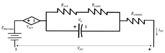
Figure 4.
Electrical circuit model of the PEMFC (Proton-Exchange Membrane Fuel Cell).
The Nernst voltage or the reversible voltage corresponds to the potential at the output of the FC without load. In [28] is presented a modified version of the equation of this voltage drop with a term that takes into account the temperature, while PO2 and PH2 are the partial pressures of oxygen and hydrogen, respectively. The equation from [28] is:
where T is the temperature.
Activation voltage losses have a greater impact when low currents circulate through the cell [29]. The Tafel equation is employed to describe the connection between current density and activation losses. This equation is valid if i > io.
where Vact represents the activation loss, T is the temperature of the fuel cell, IFC is the fuel cell current, and the ξ’s represent the parametric coefficients for each cell model, the oxygen concentration CO2 can be calculated as:
Concentration or diffusion losses occur when there is a change in the concentration of reactants, on the contrary of the activation losses, this has a greater impact at very high current, according to the following equation
where Vconc represents the concentration loss, B is a parametric coefficient which depends on each cell, J is the current density of the fuel cell, and Jmax is the maximum current density of the fuel cell.
The ohmic losses occur because of electrode resistance, current collectors, and polymeric membrane. They are proportional to the current that circulates in the fuel cell.
where Vohm represents the ohmic losses, IFC is the fuel cell current, RC is the resistance of the transfer of protons through the membrane with a value of 300 µΩ and RM is the resistance of the membrane calculated by:
The polarization curve of the fuel cell is shown in Figure 5. This type of graphic indicates the different voltages in the fuel cell model (see Figure 4) vs. the current density [30]. When the current density at the fuel cell changes, the Nerst voltage stays constant, but the fuel cell voltage VFC decreases as the current density is increasing. The different voltage drops—activation, concentration, and ohmic losses are also represented in Figure 5, to have an idea of their behavior. The parameters of the Avista fuel cell stack 500 W are shown in Table 1.
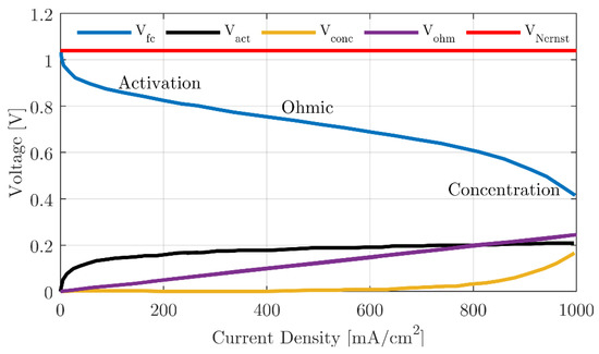
Figure 5.
Polarization curve of the PEMFC.

Table 1.
Avista 500-W Fuel Cell stack parameters.
7. Experimental Results
In this section, we show the experimental results of the proposed controller using the hardware-in-the-loop FC implementation. In Figure 6, we show a picture of the experimental prototype and the DSP that implements the proposed discrete time input current controller. The full set of parameters of the experimental setup is shown in Table 2.
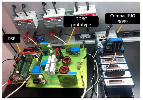
Figure 6.
Picture of the implementation of the proposed input current controller.
Table 2.
Experimental setup parameters.
We first proceed to validate the hardware-in-the-loop implementation of the FC described in the previous section. In Figure 7, we show the dynamic response of the implemented FC with respect to continuous load variations. Several experimental measurements were performed to validate the corresponding values of the characteristic curve of the FC. These measurements are illustrated in Figure 8. Moreover, experimental measurements of some of the points A, B, and C in Figure 8 are shown in Figure 9, Figure 10 and Figure 11, respectively.
Figure 7.
Dynamic response of the Fuel cell (FC) with respect to load variations.
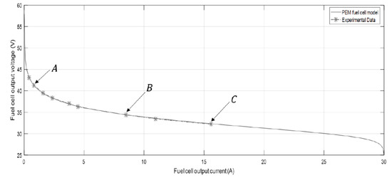
Figure 8.
Comparison between experimental and ideal current/voltage values of the implemented FC.
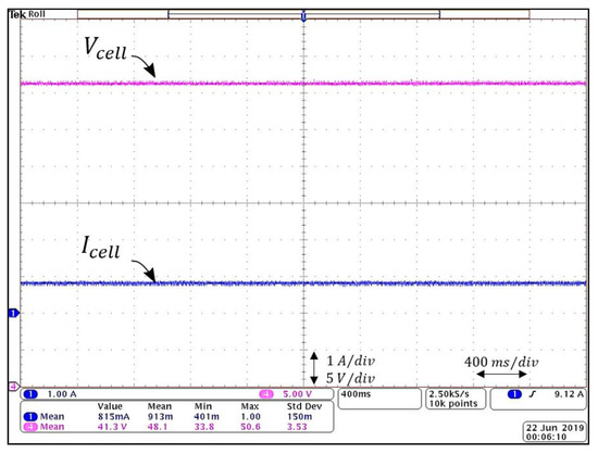
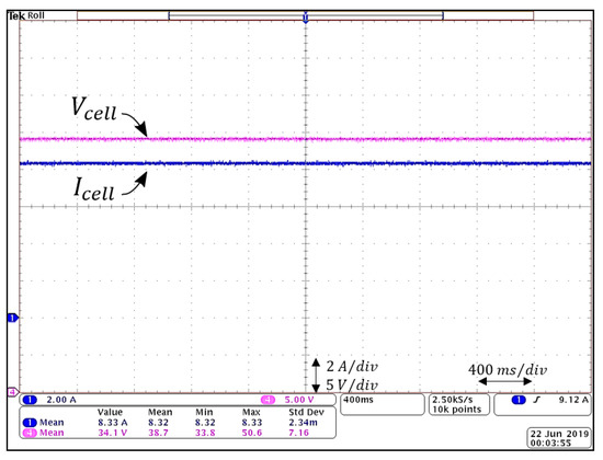
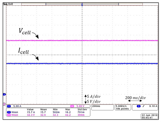
Moreover, additional measurements of the fuel cell are illustrated in Figure 8, where each point (A, B, C, D) corresponds to an operational point of the fuel cell. Points A, B, and C in Figure 8 are shown in Figure 9, Figure 10 and Figure 11, respectively, which demonstrate that the fuel cell implementation used in this paper corresponds to a real fuel cell.
Experimental results of the proposed current-controller with simultaneous cancellation of input current and output voltage ripples are shown in Figure 12 for an input current set-point of Iin = 8 A. As can be seen, the current from both inductors and the input current of the converter (output current of the fuel cell) is shown, the input current () is almost pure DC component; this is the result of the design of the converter and the control loop, which ensures that the duty cycles preserves the relation “”. A comparison between Figure 3, where equal inductors are considered, and Figure 12, where the proposed design and control scheme is employed, the improvement in the input current ripple is clear.
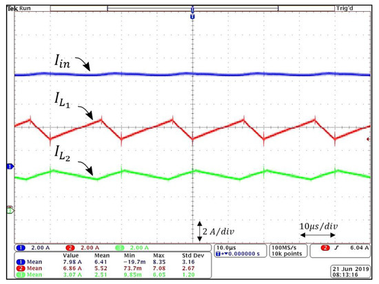
Figure 12.
Graphic of currents through inductors and the input under the proposed input current control and ripple cancellation with Iin = 8 A as set-point.
Figure 13 shows the output voltage of the converter, the output of each capacitor is shown since capacitors of the prototype have the relation “” between them, similar to the input current ripple the output voltage () is a pure DC component.
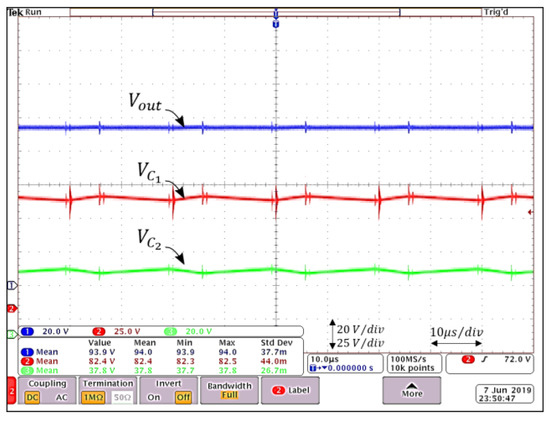
Figure 13.
Graphic of voltages across capacitors and the output under the proposed input current control and ripple cancellation with Iin = 8A as set-point.
The control over disturbances is demonstrated in Figure 14 and Figure 15; in Figure 14, a step-down voltage of 30% was made; as can be seen, the control ensures that the minimum current ripple is achieved. In Figure 15, a load variation is considered; even when a load variation is present, the current ripple remains at its minimum.
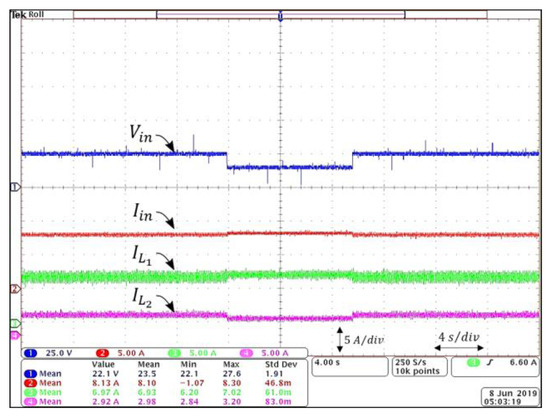
Figure 14.
Dynamic compensation of the input current under variations in the input voltage.
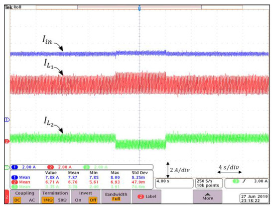
Figure 15.
Dynamic compensation of the input current under load variations.
8. Conclusions
This paper presented the implementation of a fuel cell generation system. The base of the designed system is a dc–dc double dual boost converter. The implementation includes the design and experimental validation of the converter, along with the design and validation of a closed-loop digital controller. The designed controller, in coordination with a particular selection of inductors and capacitors, minimizes the switching ripple on the topology, both switching ripples, the input current ripple and the output voltage ripple.
The work includes a complex hardware-in-the-loop experiment, with a fuel cell emulator. The emulator utilizes a controlled power source driven with a CompactRio data acquisition system. The computer program ensures the emulator behaves like a fuel cell. The mathematical model was programmed in LabView. The output of the fuel cell emulator is connected to the double dual boost converter; this particular topology of converter provides a larger voltage gain compared to the traditional boost converter and a smaller input current ripple.
The double dual boost converter was designed with a particular hardware design and operated with a particular PWM; a digital controller was developed for this application and implemented on a Texas Instruments TMS320F28335 digital signal processor.
The full experiment was developed in order to demonstrate that the double dual boost converter under the particular hardware design and the developed digital controller is able to interact with a fuel cell and provides good performance when operated in a fuel cell-based energy generation system.
The developed digital controller considers the relation among duty rations, contributing to the switching ripple minimization in both the input current and output voltage, the control must be coordinated with the selection of passive components (inductors and capacitors). This technique encompasses both a design procedure and a PWM strategy for which the designer can freely select the gain at which the input current ripple is canceled. We presented the procedure to achieve this ripple cancellation and showed that an unconstrained selection of the operating region of the converter could be achieved. This technique encompasses both a design procedure and a novel control constraint using the PWM strategy. The control loop was designed considering a small-signal discrete model, and PI converters were tuned according to a Lyapunov stabilization condition that ensures the robustness of the system against disturbances.
The proposed scheme was tested using a fuel cell emulator using Labview in a hardware-in-the-loop fashion. Experimental results from this emulation are presented to corroborate that the behavior is close enough to a real fuel cell. It is demonstrated how the control loop ensures that the ripple mitigation technique is achieved even when the system is subjected to disturbances.
Author Contributions
Authors J.C.R.-C., A.V.-G., and P.M.G.-V., contributed with the conceptualization of the article, from the power electronics point of view, J.C.M.-M. and J.E.V.-R. contributed with the control methodology, C.A.V.-H., J.L.-C., and P.M.G.-V. contributed with the software, validation, and formal analysis, C.A.V.-H. and J.C.R.-C. wrote the draft and manuscript preparation. All authors have read and agreed to the published version of the manuscript.
Funding
This research was partially funded by Universidad Panamericana, through the program “Fomento a la Investigación UP 2020”, and project “Análisis de convertidores duales dobles” UP-CI-2020-GDL-01-ING. The APC was partially funded by the aforementioned project and partially by the Universidad Panamericana Dirección Institucional de Investigación.
Conflicts of Interest
The authors declare no conflict of interest.
References
- Tseng, K.; Huang, C. High Step-Up High-Efficiency Interleaved Converter With Voltage Multiplier Module for Renewable Energy System. IEEE Trans. Ind. Electron. 2014, 61, 1311–1319. [Google Scholar] [CrossRef]
- Seok, H.; Han, B.; Kwon, B.; Kim, M. High Step-Up Resonant DC–DC Converter With Ripple-Free Input Current for Renewable Energy Systems. IEEE Trans. Ind. Electron. 2018, 65, 8543–8552. [Google Scholar] [CrossRef]
- Thounthong, P.; Davat, B.; Rael, S.; Sethakul, P. Fuel cell high-power applications. IEEE Ind. Electron. Mag. 2009, 3, 32–46. [Google Scholar]
- Arango, E.; Ramos-Paja, C.A.; Calvente, J.; Giral, R.; Serna, S. Asymmetrical Interleaved DC/DC Switching Converters for Photovoltaic and Fuel Cell Applications—Part 1: Circuit Generation, Analysis and Design. Energies 2012, 5, 4590–4623. [Google Scholar] [CrossRef]
- Somaiah, B.; Agarwal, V.; Choudhury, S.R.; Duttagupta, S.P.; Govindan, K. Analysis and comparative study of pulsating current of fuel cells by inverter load with different power converter topologies. Int. J. Hydrogen Energy 2011, 36, 15018–15028. [Google Scholar] [CrossRef]
- Valdez-Resendiz, J.E.; Sanchez, V.M.; Rosas-Caro, J.C.; Mayo-Maldonado, J.C.; Sierra, J.; Barbosa, R. Continuous input-current buck-boost dc-dc converter for pem fuel cell applications. Int. J. Hydrogen Energy 2017, 42, 30389–30399. [Google Scholar] [CrossRef]
- Guilbert, D.; Collura, S.M.; Scipioni, A. Dc/dc converter topologies for electrolyzers: State-of-the-art and remaining key issues. Int. J. Hydrogen Energy 2017, 42, 23966–23985. [Google Scholar] [CrossRef]
- Guilbert, D.; Gaillard, A.; Mohammadi, A.; N’Diaye, A.; Djerdir, A. Investigation of the interactions between proton exchange membrane fuel cell and interleaved dc/dc boost converter in case of power switch faults. Int. J. Hydrogen Energy 2015, 40, 519–537. [Google Scholar] [CrossRef]
- Kuo, J.K.; Wang, C.F. An integrated simulation model for pem fuel cell power systems with a buck dc-dc converter. Int. J. Hydrogen Energy 2011, 36, 11846–11855. [Google Scholar] [CrossRef]
- Wang, Y.; Qiu, Y.; Bian, Q.; Guan, Y.; Xu, D. A single switch quadratic boost high step up dc-dc converter. IEEE Trans. Ind. Electron. 2019, 66, 4387–4397. [Google Scholar] [CrossRef]
- Leyva-Ramos, J.; Mota-Varona, R.; Ortiz-Lopez, M.G.; Diaz-Saldierna, L.H.; Langarica-Cordoba, D. Control strategy of a quadratic boost converter with voltage multiplier cell for high-voltage gain. IEEE J. Emerg. Sel. Top. Power Electron. 2017, 5, 1761–1770. [Google Scholar] [CrossRef]
- Jiang, W.; Chincholkar, S.H.; Chan, C. Investigation of a voltage-mode controller for a dc-dc multilevel boost converter. IEEE Trans. Circuits Syst. I 2018, 65, 908–912. [Google Scholar] [CrossRef]
- Busquets-Monge, S.; Alepuz, S.; Bordonau, J. A bidirectional multilevel boost-buck dc-dc converter. IEEE Trans. Power Electron. 2011, 26, 2172–2183. [Google Scholar] [CrossRef]
- Zhu, X.; Zhang, B.; Li, Z.; Li, H.; Ran, L. Extended switched-boost dc-dc converters adopting switched-capacitor/switched-inductor cells for high step-up conversion. IEEE J. Emerg. Sel. Top. Power Electron. 2017, 5, 1020–1030. [Google Scholar] [CrossRef]
- Axelrod, B.; Berkovich, Y.; Ioinovici, A. Switched-capacitor/switched-inductor structures for getting transformerless hybrid dc-dc pwm converters. IEEE Trans. Circuits Syst. I 2008, 55, 687–696. [Google Scholar] [CrossRef]
- Lu, S.; Mu, M.; Jiao, Y.; Lee, F.C.; Zhao, Z. Coupled inductors in interleaved multiphase three-level dc-dc converter for high-power applications. IEEE Trans. Power Electron. 2016, 31, 120–134. [Google Scholar] [CrossRef]
- Jin, X.; Wang, L.; Yu, D.; Geng, Y.; Xu, R. Pulse train controlled single-input dual-output buck converter with coupled inductors. IEEE Access 2018, 6, 41504–41517. [Google Scholar] [CrossRef]
- Stala, R.; Waradzyn, Z.; Penczek, A.; Mondzik, A.; Skala, A. A switched-capacitor dc-dc converter with variable number of voltage gains and fault-tolerant operation. IEEE Trans. Ind. Electron. 2019, 66, 3435–3445. [Google Scholar] [CrossRef]
- Kawa, A.; Stala, R.; Mondzik, A.; Pirog, S.; Penczek, A. High-power thyristor-based dc-dc switched-capacitor voltage multipliers: Basic concept and novel derived topology with reduced number of switches. IEEE Trans. Power Electron. 2016, 31, 6797–6813. [Google Scholar] [CrossRef]
- Viet, D.B.; Lembeye, Y.; Ferrieux, J.P.; Barbaroux, J.; Avenas, Y. New high power—high ratio non isolated DC-DC boost converter for Fuel cell applications. In Proceedings of the 37th IEEE Power Electronics Specialists Conference, Jeju, Korea, 18–22 June 2006; pp. 1–7. [Google Scholar]
- Zhuo, S.; Gaillard, A.; Li, Q.; MA, R.; Paire, D.; Gao, F. Current Ripple Optimization of Four-Phase Floating Interleaved DC-DC Boost Converter under Switch Fault. IEEE Trans. Ind. Appl. 2020, 56, 4214–4224. [Google Scholar] [CrossRef]
- Kabalo, M.; Paire, D.; Blunier, B.; Bouquain, D.; Simões, M.G.; Miraoui, A. Experimental evaluation of four-phase floating interleaved boost converter design and control for fuel cell applications. IET Power Electron. 2013, 6, 215–226. [Google Scholar] [CrossRef]
- Valdez-Resendiz, J.E.; Rosas-Caro, J.C.; Mayo-Maldonado, J.C.; Calderon-Zavala, G.; Valderrabano-Gonzalez, A.; Escobar-Valderrama, G. Voltage and Current Switching-Ripple Cancelation in the Double Dual Boost Converter. In Proceedings of the 14th International Conference on Power Electronics (CIEP), Cholula, Mexico, 24–26 October 2018; pp. 89–95. [Google Scholar]
- Polderman, J.; Willems, J. Introduction to Mathematical System Theory: A Behavioral Approach; Springer: Berlin/Heidelberg, Germany, 1997. [Google Scholar]
- Papageorgiou, C.; Smith, M.C. Positive real synthesis using matrix inequalities for mechanical networks: Application to vehicle suspension. IEEE Trans Control Syst. Technol. 2006, 14, 423–435. [Google Scholar] [CrossRef]
- Gebregergis, A.; Pillay, P. Implementation of fuel cell emulation on dspand dspace controllers in the design of power electronic converters. In Proceedings of the IEEE Industry Applications Society Annual Meeting, Portland, OR, USA, 23–27 September 2018; pp. 1–8. [Google Scholar]
- Wang, C.; Nehrir, M.H.; Shaw, S.R. Dynamic models and model validation for pem fuel cells using electrical circuits. IEEE Trans. Energy Convers. 2005, 20, 442–451. [Google Scholar] [CrossRef]
- Voottipruex, K.; Sangswang, A.; Naetiladdanon, S.; Mujjalinvimut, E.; Wongyoa, N. Pem fuel cell emulator based on dynamic model with relative humidity calculation. In Proceedings of the 14th International Conference on Electrical Engineering/Electronics, Computer, Telecommunications and Information Technology (ECTI-CON), Phuket, Thailand, 27–30 June 2017; pp. 529–532. [Google Scholar]
- Lee, H.S.; Jeong, K.S.; Oh, B.S. An experimental study of controlling strategies and drive forces for hydrogen fuel cell hybrid vehicles. Int. J. Hydrogen Energy 2003, 28, 215–222. [Google Scholar] [CrossRef]
- Kunusch, C.; Puleston, P.; Mayosky, M. PEM Fuel Cell Systems. In Sliding-Mode Control of PEM Fuel Cells. Advances in Industrial Control; Springer: London, UK, 2012. [Google Scholar]
© 2020 by the authors. Licensee MDPI, Basel, Switzerland. This article is an open access article distributed under the terms and conditions of the Creative Commons Attribution (CC BY) license (http://creativecommons.org/licenses/by/4.0/).