Design and Validation of 100 nm GaN-On-Si Ka-Band LNA Based on Custom Noise and Small Signal Models

 ,
,  ,
,  , ,
, ,  ,
,
Abstract
1. Introduction
2. Chosen Technology
2.1. Description
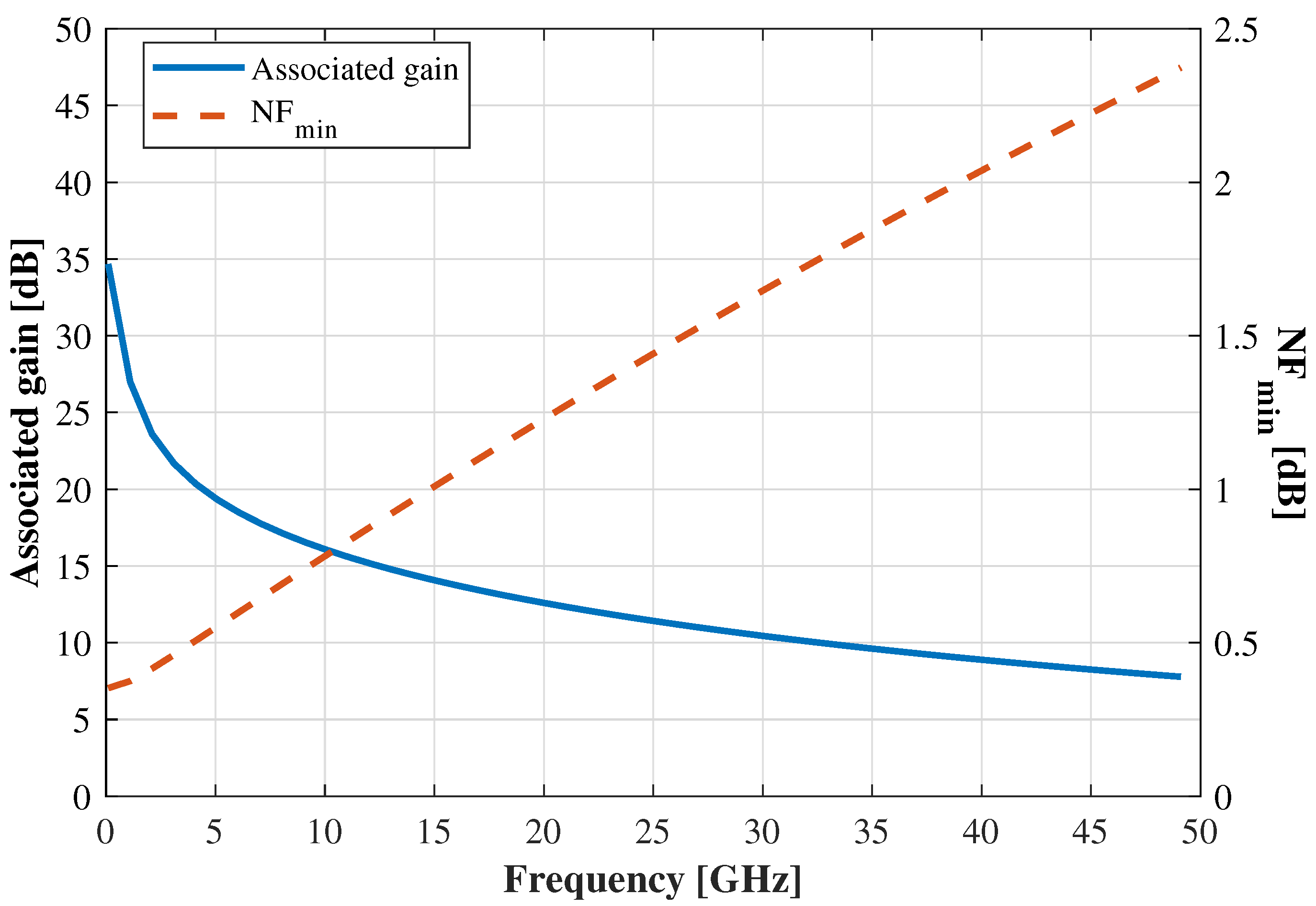
2.2. Modelling
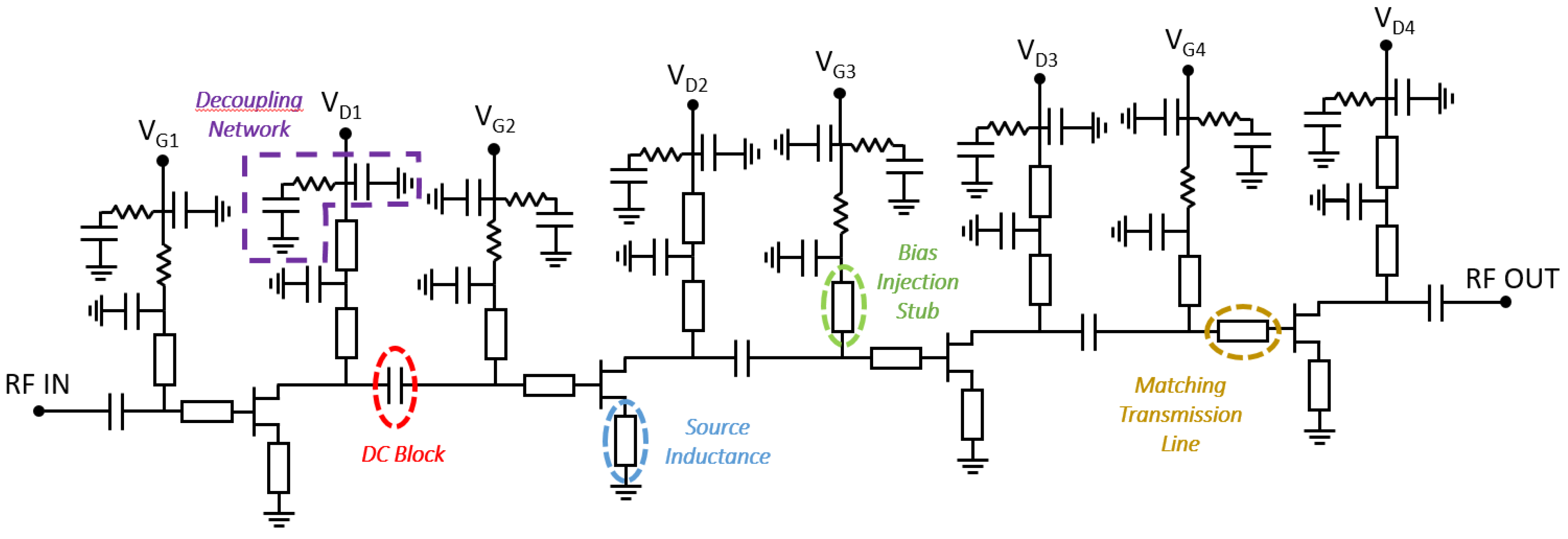
3. Test Vehicle Design
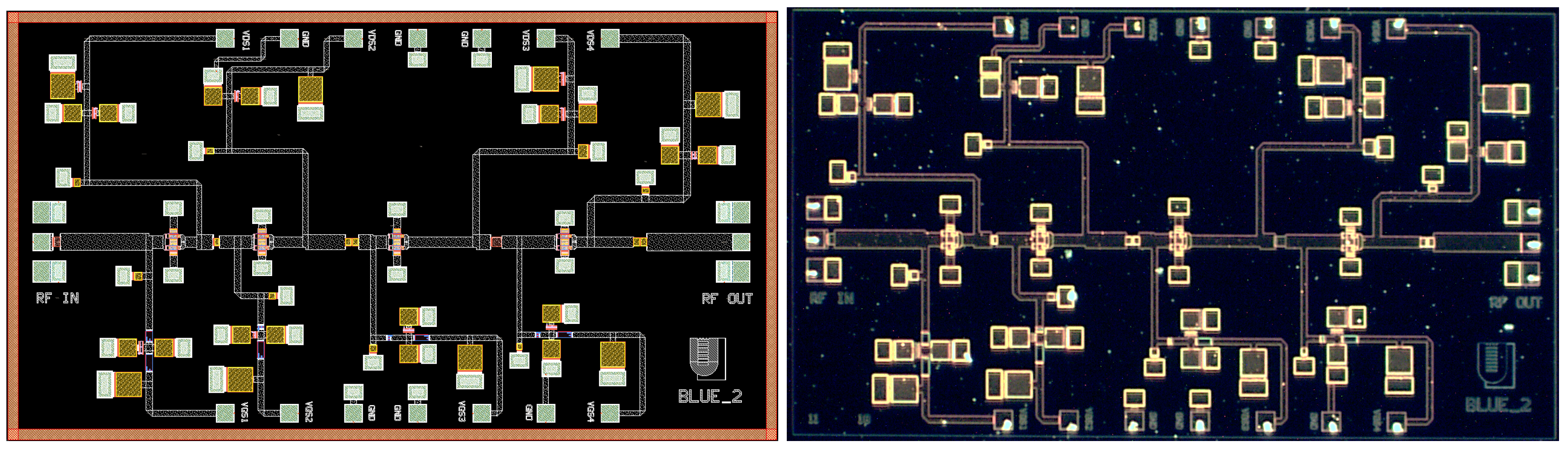
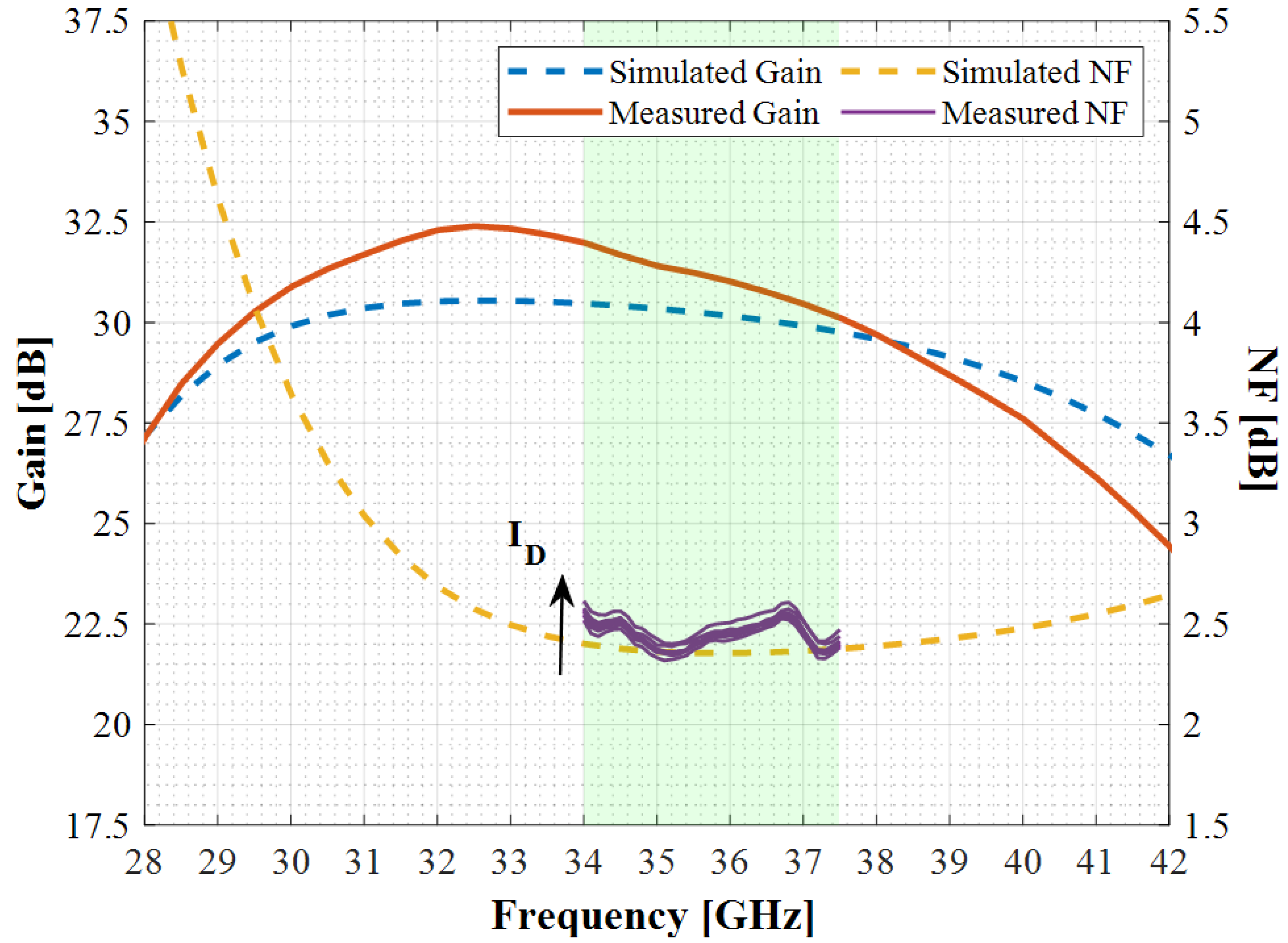
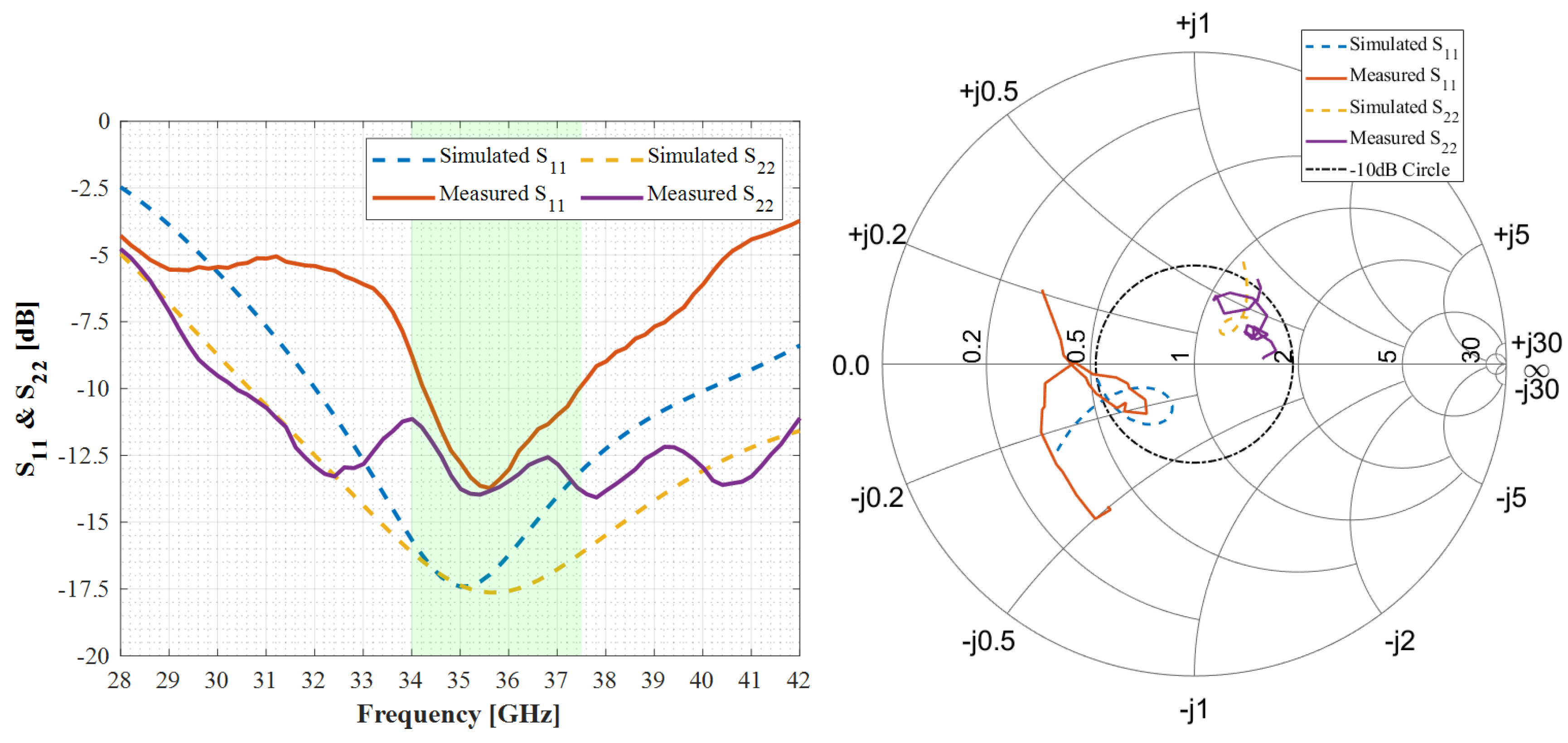
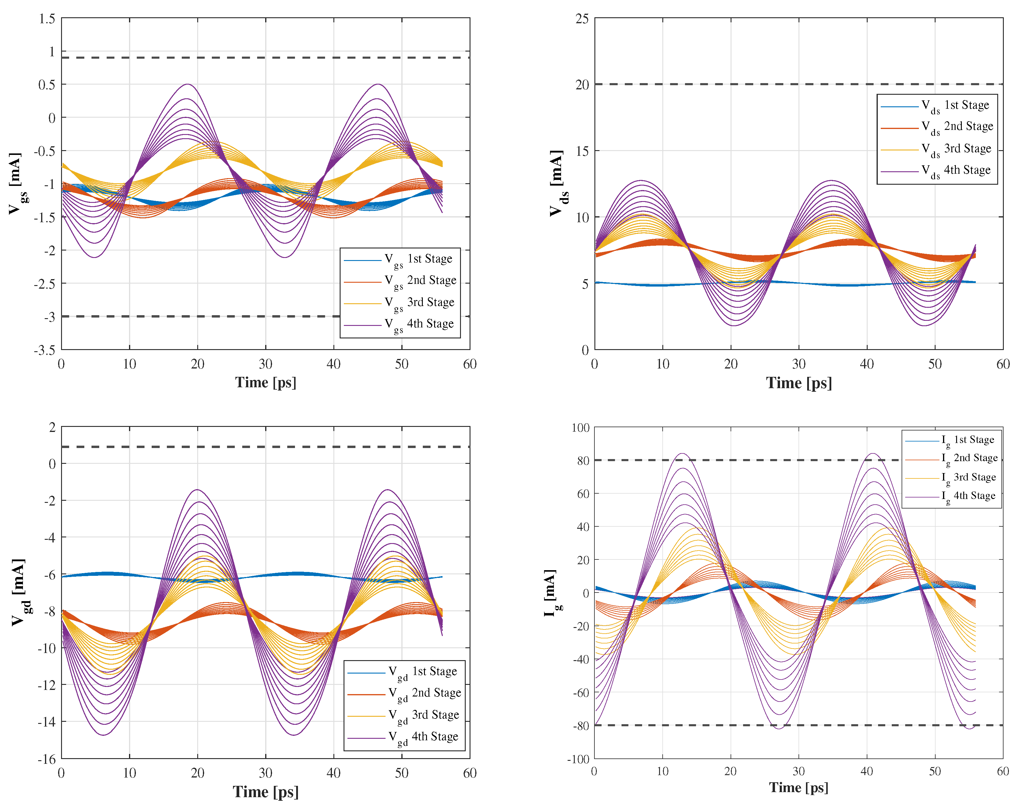
4. Layout and Performance
5. Conclusions
Author Contributions
Funding
Conflicts of Interest
Abbreviations
| DC | Direct current |
| EM | Electromagnetic |
| GaAs | Gallium arsenide |
| GaN | Gallium nitride |
| HEMT | High electron mobility transistor |
| HPA | High power amplifier |
| IC | Integrated circuit |
| IMN | Input matching network |
| ISMN | Inter-stage matching network |
| LNA | Low-noise amplifier |
| LRRM | Line reflect reflect match |
| MIM | Metal-insulator-metal |
| MMIC | Microwave monolithic integrated circuit |
| NF | Noise figure |
| NFmin | Minimum noise figure |
| OIP3 | Output third harmonic intercept point |
| O1 dBcp | Output 1 dB compression point |
| RF | RadioFrequency |
| SCFE | Single-chip front-end |
| Si | Silicon |
| SiC | Silicon carbide |
| SOLT | Short open line thru |
| SPDT | Single-pole double-throw |
| TRM | Transmit-receive module |
| VNA | Vector Network analyzer |
References
- Leuther, A.; Tessmann, A.; Dammann, M.; Massler, H.; Schlechtweg, M.; Ambacher, O. 35 nm mHEMT Technology for THz and ultra low noise applications. In Proceedings of the 2013 International Conference on Indium Phosphide and Related Materials (IPRM), Kobe, Japan, 19–23 May 2013; Volume 2, pp. 1–2. [Google Scholar] [CrossRef]
- Komiak, J.J.; Smith, P.M.; Duh, K.H.G.; Xu, D.; Chao, P.C. Metamorphic HEMT technology for microwave, millimeter-wave, and submillimeter-wave applications. In Proceedings of the Technical Digest—IEEE Compound Semiconductor Integrated Circuit Symposium (CSIC), Monterey, CA, USA, 13–16 October 2013; pp. 1–4. [Google Scholar] [CrossRef]
- Ciccognani, W.; Colangeli, S.; Longhi, P.E.; Limiti, E. Design of a MMIC low-noise amplifier in industrial gallium arsenide technology for E-band 5G transceivers. Microw. Opt. Technol. Lett. 2019, 61, 205–210. [Google Scholar] [CrossRef]
- Ciccognani, W.; Longhi, P.E.; Colangeli, S.; Limiti, E. Q/V band LNA for satellite on-board space applications using a 70 nanometers GaAs mHEMT commercial technology. Microw. Opt. Technol. Lett. 2018, 60, 2185–2190. [Google Scholar] [CrossRef]
- Longhi, P.E.; Pace, L.; Colangeli, S.; Ciccognani, W.; Limiti, E. Technologies, Design, and Applications of Low-Noise Amplifiers at Millimetre-Wave: State-of-the-Art and Perspectives. Electronics 2019, 8, 1222. [Google Scholar] [CrossRef]
- Giordani, R.; Amici, M.; Barigelli, A.; Conti, F.; Del Marro, M.; Feudale, M.; Imparato, M.; Suriani, A. Highly integrated and solderless LTCC based C-band T/R module. In Proceedings of the European Microwave Week 2009, EuMW 2009: Science, Progress and Quality at Radiofrequencies, Conference Proceedings—39th European Microwave Conference (EuMC), Rome, Italy, 28–29 September 2009; pp. 1760–1763. [Google Scholar] [CrossRef]
- Ciccognani, W.; Colangeli, S.; Serino, A.; Pace, L.; Longhi, P.E.; Limiti, E.; Poulain, J.; Leblanc, R. Comparative noise investigation of high-performance GaAs and GaN millimeter-wave monolithic technologies. In Proceedings of the 14th European Microwave Integrated Circuits Conference (EuMIC), Paris, France, 29 September–2 October 2019; pp. 1–4. [Google Scholar]
- Sarazin, N.; Morvan, E.; Di Forte Poisson, M.A.; Oualli, M.; Gaquiere, C.; Jardel, O.; Drisse, O.; Tordjman, M.; Magis, M.; Delage, S.L. AlInN/AlN/GaN HEMT technology on SiC with 10-W/mm and 50% PAE at 10 GHz. IEEE Electron Device Lett. 2010, 31, 11–13. [Google Scholar] [CrossRef]
- Sun, H.; Alt, A.R.; Benedickter, H.; Feltin, E.; Carlin, J.F.; Gonschorek, M.; Grandjean, N.; Bolognesi, C.R. Low-noise microwave performance of 0.1 µm gate AlInN/GaN HEMTs on SiC. IEEE Microw. Wirel. Components Lett. 2010, 20, 453–455. [Google Scholar] [CrossRef]
- Palombini, D.; Rampazzo, D.; Bentini, A.; Longhi, P.E. Design of a 5W Single Chip Front-End for C-Ku Band T/R Modules. In Proceedings of the IEEE MTT-S International Microwave Symposium Digest, Philadelphia, PA, USA, 10–15 June 2018; pp. 647–650. [Google Scholar] [CrossRef]
- Limiti, E.; Colangeli, S.; Bentini, A.; Nanni, A. Characterization and modeling of low-cost, high-performance GaN-Si technology. In Proceedings of the 2012 19th International Conference on Microwaves, Radar and Wireless Communications, MIKON 2012, Warsaw, Poland, 21–23 May 2012; Volume 2, pp. 599–604. [Google Scholar] [CrossRef]
- Hilt, O.; Zhytnytska, R.; Böcker, J.; Bahat-Treidel, E.; Brunner, F.; Knauer, A.; Dieckerhoff, S.; Würfl, J. 70 mΩ/600 V normally-off GaN transistors on SiC and Si substrates. In Proceedings of the 2015 IEEE 27th International Symposium on Power Semiconductor Devices and IC’s (ISPSD), Hong Kong, China, 10–14 May 2015; Volume 2015, pp. 237–240. [Google Scholar] [CrossRef]
- De Padova, A.; Longhi, P.E.; Colangeli, S.; Ciccognani, W.; Limiti, E. Design of a GaN-on-Si Single-Balanced Resistive Mixer for Ka-band Satcom. IEEE Microwav. Wirel. Compon. Lett. 2019, 29, 56–58. [Google Scholar] [CrossRef]
- Pace, L.; Ciccognani, W.; Colangeli, S.; Longhi, P.E.; Limiti, E.; Leblanc, R. A Ka-Band Low-Noise Amplifier for Space Applications in a 100 nm GaN on Si technology. In Proceedings of the PRIME 2019 15th Conference on Ph.D. Research in Microelectronics and Electronics, Lausanne, Switzerland, 15–18 July 2019; pp. 161–164. [Google Scholar] [CrossRef]
- Reveyrand, T.; Ciccognani, W.; Ghione, G.; Jardel, O.; Limiti, E.; Serino, A.; Camarchia, V.; Cappelluti, F.; Quéré, R. GaN transistor characterization and modeling activities performed within the frame of the KorriGaN project. Int. J. Microw. Wirel. Technol. 2010, 2, 51–61. [Google Scholar] [CrossRef]
- Colangeli, S.; Longhi, P.E.; Ciccognani, W.; Limiti, E. On the Optimum Noise-Gain Locus of Two-Ports. IEEE Trans. Microw. Theory Tech. 2019, 67, 2284–2290. [Google Scholar] [CrossRef]
- Salvucci, A.; Longhi, P.E.; Colangeli, S.; Ciccognani, W.; Serino, A.; Limiti, E. A straightforward design technique for narrowband multi-stage low-noise amplifiers with I/O conjugate match. Int. J. Microw.-Comput.-Aided Eng. 2019, 29, e21833. [Google Scholar] [CrossRef]
- Nsele, S.D.; Robin, C.; Tartarin, J.G.; Escotte, L.; Piotrowicz, S.; Jardel, O.; Delage, S. Ka-band low noise amplifiers based on InAlN/GaN technologies. In Proceedings of the 2015 International Conference on Noise and Fluctuations, Xi’an, China, 2–6 June 2015; pp. 1–4. [Google Scholar] [CrossRef]
- Suijker, E.M.; Rodenburg, M.; Hoogland, J.A.; Van Heijningen, M.; Seelmann-Eggebert, M.; Quay, R.; Brückner, P.; Van Vliet, F.E. Robust AlGaN/GaN low noise amplifier MMICs for C-, Ku- and Ka-band space applications. In Proceedings of the Technical Digest—IEEE Compound Semiconductor Integrated Circuit Symposium, CSIC, Greensboro, NC, USA, 11–14 October 2009; pp. 3–6. [Google Scholar] [CrossRef]
- Rudolph, M.; Chaturvedi, N.; Hirche, K.; Würfl, J.; Heinrich, W.; Tränkle, G. Highly rugged 30 GHz GaN low-noise amplifiers. IEEE Microw. Wirel. Compon. Lett. 2009, 19, 251–253. [Google Scholar] [CrossRef]
- Micovic, M.; Brown, D.; Regan, D.; Wong, J.; Tai, J.; Kurdoghlian, A.; Herrault, F.; Tang, Y.; Burnham, S.D.; Fung, H.; et al. Ka-Band LNA MMIC’s Realized in Fmax > 580 GHz GaN HEMT Technology. In Proceedings of the Technical Digest—IEEE Compound Semiconductor Integrated Circuit Symposium, CSIC, Austin, TX, USA, 23–26 October 2016; pp. 1–4. [Google Scholar] [CrossRef]
- Fung, A.; Hoffman, J.; Aguirre, F.; Horst, S. Development of Gallium Nitride Monolithic Microwave Circuits for the Modular Dual-Band Ku/Ka Antenna Tile with Digital Calibration (K-Tile). Presentacion, 14–16 June 2016. [Google Scholar]


| Parameter | Unit | Value |
|---|---|---|
| Gate Length | nm | 100 |
| Substrate Thickness | µm | 100 |
| fT | GHz | 110 |
| fMAX | GHz | 160 |
| RF Power Density | W/mm | 3.3 |
| Transconductance | mS/mm | 800 |
| Noise Figure @ 40GHz | dB | 1.5 |
| IDss Max | A/mm | 1.7 |
| Breakdown VGD | V | 36 |
| VDD for best noise | V | 3 to 7 |
| VDD for power | V | 12 to 13 |
| Parameter | Unit | Value |
|---|---|---|
| Frequency | GHz | 34 to 37.5 |
| Linear Gain | dB | ≥30 |
| Noise Figure | dB | ≤2.5 |
| I/O Return Loss | dB | ≥10 |
| Output 1dBcp | dBm | ≥20 |
| Unit | 1st stg | 2nd stg | 3rd stg | 4th stg | |
|---|---|---|---|---|---|
| Periphery | µm | 4 × 35 | 4 × 35 | 4 × 35 | 4 × 35 |
| VDD | V | 5 | 7.5 | 7.5 | 7.5 |
| ID | mA | 16 | 25 | 69 | 69 |
| PDC | W | 0.08 | 0.18 | 0.52 | 0.52 |
| Parameter | Unit | Value |
|---|---|---|
| Vgd | V | −30 to +0.9 |
| Vgs | V | −3 to +0.9 |
| Vds | V | −20 to +20 |
| Ig | DC mA/finger | 2 |
| Ig | DC + RF mA/finger | 20 |
| Ka-Band GaN LNAs | Unit | [18] | [19] | [20] | [21] | [22] | This Work |
|---|---|---|---|---|---|---|---|
| Substrate | SiC | SiC | SiC | SiC | Si | Si | |
| Gate Length | [nm] | 150 | 150 | 150 | 40 | 150 | 100 |
| Frequency | [GHz] | 25 to 35 | 27.5 to 28.5 | 27 to 31 | 27 to 40 | 35.5 | 34 to 37.5 |
| Avg Gain | [dB] | ≥20 | 18 | ≤20 | ≤27 | 17 | 31 |
| Avg NF | [dB] | ≥3 | 4 | ≤3.9 | ≤1.6 | 2.9 | 2.4 |
| I/O Return Loss | [dB] | ≥10 | ≥6.5 | ≥7 | ≥5 | ≥9 | ≥10 |
| Output 1dBcp | [dBm] | - | ≥12.5 | - | 11 | - | 23 |
| PDC | [W] | 0.36 | 0.2 | - | 0.082 | 0.3 | 1.3 |
| O1dBcp/PDC | [%] | - | 8.9 | - | 15.3 | - | 19 |
| Size | [mm2] | 2.6 × 0.8 | 3 × 2 | 3.4 × 1.2 | 3.1 × 1.12 | - | 3.6 × 2 |
© 2020 by the authors. Licensee MDPI, Basel, Switzerland. This article is an open access article distributed under the terms and conditions of the Creative Commons Attribution (CC BY) license (http://creativecommons.org/licenses/by/4.0/).
Share and Cite
Pace, L.; Colangeli, S.; Ciccognani, W.; Longhi, P.E.; Limiti, E.; Leblanc, R.; Feudale, M.; Vitobello, F. Design and Validation of 100 nm GaN-On-Si Ka-Band LNA Based on Custom Noise and Small Signal Models. Electronics 2020, 9, 150. https://doi.org/10.3390/electronics9010150
Pace L, Colangeli S, Ciccognani W, Longhi PE, Limiti E, Leblanc R, Feudale M, Vitobello F. Design and Validation of 100 nm GaN-On-Si Ka-Band LNA Based on Custom Noise and Small Signal Models. Electronics. 2020; 9(1):150. https://doi.org/10.3390/electronics9010150
Chicago/Turabian StylePace, Lorenzo, Sergio Colangeli, Walter Ciccognani, Patrick Ettore Longhi, Ernesto Limiti, Remy Leblanc, Marziale Feudale, and Fabio Vitobello. 2020. "Design and Validation of 100 nm GaN-On-Si Ka-Band LNA Based on Custom Noise and Small Signal Models" Electronics 9, no. 1: 150. https://doi.org/10.3390/electronics9010150
APA StylePace, L., Colangeli, S., Ciccognani, W., Longhi, P. E., Limiti, E., Leblanc, R., Feudale, M., & Vitobello, F. (2020). Design and Validation of 100 nm GaN-On-Si Ka-Band LNA Based on Custom Noise and Small Signal Models. Electronics, 9(1), 150. https://doi.org/10.3390/electronics9010150