Abstract
A new reduced form-factor three axes digital teslameter, based on the spinning current technique, has been developed. This instrument will be used to characterize the SwissFEL insertion devices at the Paul Scherrer Institute (PSI) for the ATHOS soft X-ray beamline. A detailed and standardized calibration procedure is critical to optimize the performance of this precision instrument. This paper presents the measurement techniques used for the corrective improvements implemented through non-linearity, temperature offset, temperature sensitivity compensation of the Hall probe and electronics temperature compensation. A detailed quantitative analysis of the reduction in errors on the application of each step of the calibration is presented. The percentage peak error reduction attained through calibration of the instrument for reference fields in the range of ±2 T is registered to drop from 1.94% down to 0.02%.
1. Introduction
Most Hall probe sensors consist of n-type semiconductors made of single elements like Si and III-V compounds like InSb, InAs and GaAs. Silicon has moderate electron mobility but is compatible with integrated circuit technology making it the ideal choice for the realization of Hall sensor chips [1].
The quality of a Hall probe is mostly determined by its low zero field offset, its drift with time, its sensitivity to the magnetic field, the magnitude of the linearity error of the output Hall voltage and the minimization of the thermal, electrical and frequency noise.
As explained in References [1,2,3,4] the offset voltage is the parasitic output voltage that appears in the absence of a magnetic field. This mostly originates from the structural asymmetry in the geometry and non-uniform doping densities of the active part of the sensor. This offset can also drift with time due to the ageing of the semiconductor material especially in cryogenic application conditions. Thermal cycles also cause micro cracks in the active area of the sensor and mechanical stresses that change the Hall coefficient.
The sensitivity of the Hall probe is temperature dependent due to the thermal activated behavior of the carrier concentration whose density increases with temperature. This is especially true if the Hall element is composed of a material with a small band-gap like InSb as explained in Reference [1].
The Hall voltage measurement output is not a linear function of the magnetic field density. This nonlinear behavior is mainly caused by the field dependence of the Hall coefficient RH that is related to the density of the electrons inside the support material and its mobility.
The main limitation of the measurement precision of a Hall probe is the noise that appears at the output of the signal voltage. Johnson-Nyquist noise results from the thermally induced motion of the electrons in the material which is defined by Equation (1) where k is the Boltzmann constant (1.38 × 10⁻²³ JK−1), T is the absolute temperature in K, R is the resistance in ohms and BW is the bandwidth in hertz.
Limitation of this source of noise is maintained by keeping the bandwidth as low as possible. An additional noise source is flicker noise which is dominant at very low frequencies. This depends on the material and on the fabrication technique of the Hall element which can be improved.
The planar Hall effect [1,2,3,4] is a galvanomagnetic effect which corresponds to an induced electric field perpendicular to the current in the current-magnetic field plane of the Hall sensor die. This voltage is induced when the Hall device is exposed to a non-orthogonal magnetic field and thus adds up to the true Hall voltage. This offset voltage depends on the magnetic field and is proportional to the square of the planar field Bp.
2. Spinning Current Modulation Technique
Since Hall sensors suffer from offsets due to various factors as explained previously, proper interfacing circuitry that minimizes these offset effects is necessary. One method that is used is pairing two matched sensors and connect them electrically in parallel but with orthogonal current directions as in References [1,3]. The equivalent circuit of a Wheatstone bridge sensor is shown in Figure 1. Proper offset cancellation is possible if the two sensors have exactly matching properties. However, this is very difficult to achieve in practice. Electrically this matching implies that the change in the resistance that appears in one leg of the bridge must be equivalent in the two sensors.
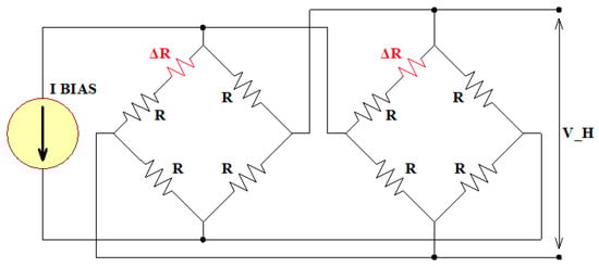
Figure 1.
Pairing of two matched sensors being connected electrically in parallel but having orthogonal current directions.
Because this technique is limited by the mismatching between the Hall devices, compensation of offsets and drifts is only partial. Through the advancement of analog signal processing, the spinning current modulation technique was developed [1,2,3,4,5,6] which allows dynamic cancellation of the offset and low frequency noise through a quick periodic exchange of the bias and sense terminals of the Hall plate.
As shown in Figure 2, the output voltage between points “C” and “D” is Vout1 = VH + Voffs, while in the second cycle the connections are commutated and an output voltage of Vout2 = VH − Voffs is recorded between points “A” and “B.” The difference between the mean values Vout1 and Vout2 is equivalent to VH. The offset reduction is achieved by the fact that only the Hall voltage depends on the current direction but the offset voltage does not.
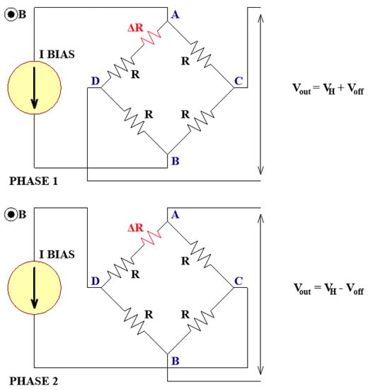
Figure 2.
Spinning Current Technique showing two phases. In phase 1 the current flows from terminal A to B and voltage is sensed between C and D, while in phase 2 the terminals are swapped and the offset voltage changes polarity.
3. Architecture of the Teslameter
The full development of the new teslameter can be found in Reference [7] with details pertaining to the actual architecture and operation capabilities of the instrument itself. As an extension to this, Figure 3 shows the complete artwork of the instrumentation PCB itself. In Reference [8] the actual final performance of the electronic instrumentation is explained with a brief reference to the calibration of the instrument. As the calibration is a very complex and long process this will be explained fully throughout the rest of this article.
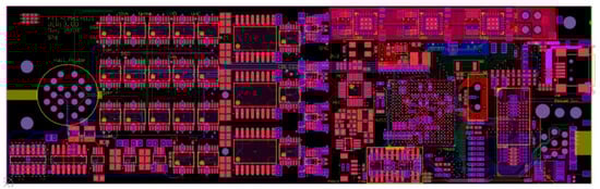
Figure 3.
Artwork of the 8 layer PCB (Printed Circuit Board) showing the 4 signal layers and the silkscreen.
4. Instrument Calibration Overview
Calibration of the instrument digital voltage outputs for the X-axis, Y-axis and Z-axis to true magnetic field values requires extensive signal processing treatment which is very difficult to perform using discrete hardware electronics. Therefore, a calibration algorithm is devised and programmed on the microcontroller which follows the block diagram structure as shown in Figure 4.
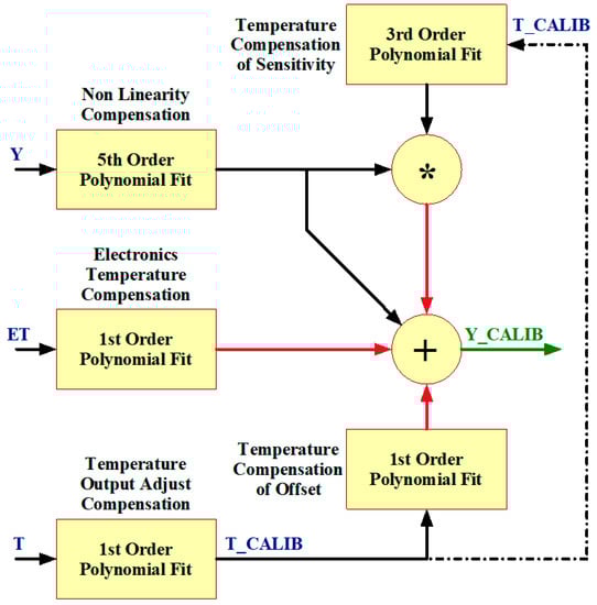
Figure 4.
Calibration block diagram showing the different blocks necessary for a complete calibration and the order of polynomials applied in modelling each block.
The roles of the yellow blocks of Figure 4 are explained as follows. The block “Nonlinearity Compensation” corrects the nonlinearity of the signal over the ±2 T magnetic field range using a 5th order polynomial. The block “Temperature Output Adjust Compensation” converts the PT100 voltage output to a true temperature reading. This is then used in the block “Temperature Compensation of Offset” which makes the temperature signal suitable for compensating the offset drift with temperature. The block “Temperature Compensation of Sensitivity” corrects the temperature influence on the sensitivity. The electronics temperature is also read by a digital sensor and this is calibrated for using a first order polynomial when the ambient temperature of the instrumentation varies from the 24 °C reference.
All the corrections are added to the signal at the point indicated by the summer in Figure 4 and the true calibrated value is output. This calibration procedure is performed individually for all three axes.
5. Calibration Procedure and Results
This section provides a detailed explanation and overview of each calibration step undertaken together with a quantitative analysis of the step improvements obtained. A LabVIEW interface was designed and coded for the end user in order to facilitate the calibration procedure. This interface allows the user to connect with the instrument through a USB connection and with the nuclear magnetic resonance (NMR) through an RS232 interface for simultaneous data acquisition. The PT2025 Metrolab NMR was used throughout the calibration procedure for magnetic field reference readings. This NMR has an absolute accuracy of ±5 ppm which could be improved by absolute calibration of the probes.
5.1. Correction of Nonlinearity
Nonlinearity compensation has the largest impact on the overall absolute accuracy of the final calibrated data given by the instrument. The Hall probe was exposed to the whole ±2 T range in 50 mT steps and the digitized voltage output from the instrument together with the actual NMR readings were recorded simultaneously. Therefore, the nonlinear relation obtained can be modelled using different orders of polynomial fits whose residual percentage errors are depicted in Figure 5 for the mean NMR plateaus over the ±2 T range.
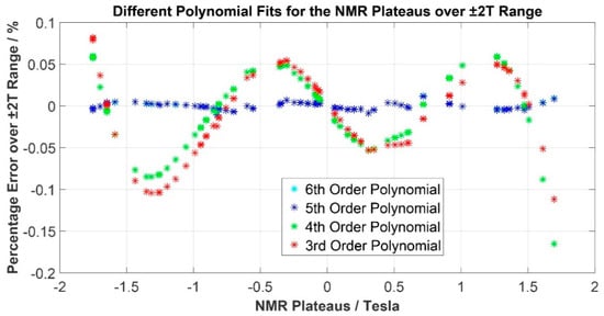
Figure 5.
The application of 3rd order to 6th order polynomial fits in modelling the nonlinear relation between the instrument output and the nuclear magnetic resonance (NMR) values. The resulting percentage error is shown for each polynomial fit.
From Figure 5 it can be concluded visually that the best percentage error achieved using a 5th order polynomial fit resides in the range of ±0.01%. Orders higher than 5 resulted in no appreciable difference in the residual error, leading to the conclusion that the 5th order polynomial provides the best trade-off between accuracy and computation complexity. This is shown in Table 1 where a tenfold improvement is registered from a 4th order polynomial to a 5th order one for the reduction in the peak error. Nonlinearity compensation is thus applied using a 5th order polynomial fit for each axis. Figure 6 shows the actual implementation of the 5th order polynomial fit on the uncalibrated data obtained versus the NMR data obtained. In order to have the best fit for the response, each NMR locked magnetic field value, subsequently called a plateau, is first filtered so that all plateaus contain the same number of points. The NMR mean and the instrument output reading mean are taken for each plateau and the polynomial fit is then found as shown in Figure 6.

Table 1.
Tabulation of percentage errors obtained for each order of polynomial fit and before any calibration is applied.
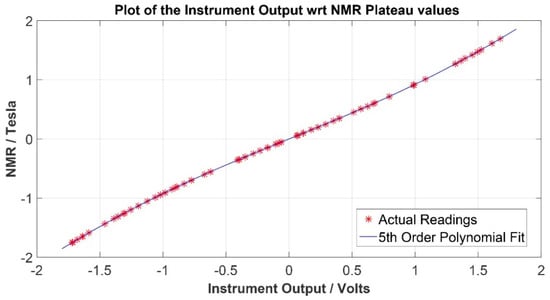
Figure 6.
Graph showing the actual mean output response of the instrument at each set NMR plateau and the fit obtained using a 5th order polynomial.
5.2. Correction of Temperature Influence
5.2.1. Temperature Output Adjust
The “Temperature Output Adjust” block converted the digitized Hall probe PT100 readings to corresponding actual temperature values for the temperature range of 15 °C up to 35 °C. Since the PT100 is a platinum resistive element with a constant positive temperature coefficient, this relationship is a linear one. This calibration block is necessary in order to feed the signal “T_CALIB” to the block “Temperature Compensation of Offset,” as shown in Figure 4, to perform the required offset compensation.
This test was carried out by varying the temperature of the Hall probe from 14 °C up to 34 °C by placing it inside a temperature controlled chamber and varying the chamber temperature in a hysteresis manner. Two temperature cycles were performed in order to verify that no drift was present. Figure 7 shows this hysteresis relation which was modelled using a linear polynomial between the Hall probe PT100 and the actual temperature of the chamber minus the ambient reference temperature at which nonlinearity compensation was performed (24 °C). We see that since the chamber temperature was being varied continuously and not stepped, the Hall probe exhibited a lagging temperature response both during heat up and cool down. This effect resulted in a temperature calibration uncertainty of around ±2 °C as shown in Figure 7.
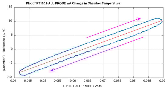
Figure 7.
Graph showing the response of the PT100 output voltage to a two cycle temperature sweep from 14 °C to 34 °C. The response is modelled using the red linear plot. Hysteresis direction is shown by the purple arrows.
5.2.2. Temperature Compensation of Offset
“Temperature Compensation of Offset” was performed by using the “T_CALIB” signal from the “Temperature Output Adjust” block and zero gauss data of the three axes from the Hall probe. The Hall probe was placed in a high permeability three layer Mu-metal chamber that provided a consistent low field test volume.
The gradient coefficient of the first order polynomial was used to obtain the required additional offset across the temperature range that must be subtracted from the already linearized magnetic field value, whose constant coefficient cancels the constant part of the offset. Figure 8 shows this relation where one can note that the slope of the relation is nearly flat with a gradient of 15.78 µT/°C and with an absolute mean value of 24 µT at 24 °C. Therefore, this block takes care of the slight change in the offset magnitude at zero gauss and ensures that irrespective of the Hall probe temperature, the field read out by the instrument is always tied to zero when the Hall probe is at zero gauss.
Figure 8.
Graph showing the variation in the output response of the instrument for the Y-axis as the Hall probe is placed in a zero gauss chamber and its temperature is varied from 19 °C up to 37 °C in a single full hysteresis cycle.
5.2.3. Temperature Compensation of Sensitivity
“Temperature Compensation of Sensitivity” caters for temperature changes across the whole magnetic field dynamic range as an addition to correcting the offset at zero gauss as performed in “Temperature Compensation of Offset” test. It is expected that the calibration error reduces more upon implementing temperature sensitivity compensation. This is due to the fact that the response of the Hall probe for temperature changes at different fields varies across the whole range. This must be modelled correctly to have a well calibrated instrument.
Temperature hysteresis sweeps were performed for locked NMR values of 0.3 T, −0.3 T, 1 T, −1 T, 1.6 T and −1.6 T while the Hall probe was heated and then cooled using a Peltier element for the temperature range of 17 °C up to 31 °C in each case. In the setup as shown in Figure 9, the NMR probe was placed on top of the Hall probe and both were sandwiched between the electromagnet poles. As the NMR probe and the Hall probe were in very close proximity to each other and the electromagnet poles were very large, it was assumed that the magnetic flux was identical in the physical region of the Hall probe and that of the NMR probe. On the right-hand side, the Peltier element was placed in physical contact with the Hall probe and one of the electromagnet poles.
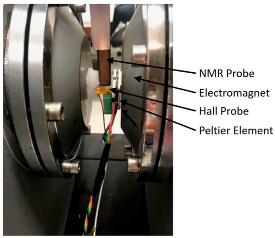
Figure 9.
Electromagnet setup showing the Hall probe placed between the poles with the NMR probe on top of it. The Peltier element is placed in physical contact with the Hall probe on the right-hand side.
The mathematical application and the determination of the nth order polynomial fit for “Temperature Compensation of Sensitivity” involves quite a detailed explanation as follows. The data acquired for the locked NMR values of 0.3 T, −0.3 T, 1 T, −1 T, 1.6 T and −1.6 T against the temperature sweeps was initially processed and linearly compensated (using a 5th order polynomial as explained in Section 5.1) to achieve magnetic field values from the digitized voltage output of the instrument for each of the three axes. By subtracting the linearized magnetic field values from the NMR readings, the actual magnetic field error against temperature was found for every plateau. The data modelling plot in Figure 10 shows the hypothetical relations that are expected for the six plateaus which show that as the NMR reading is independent of temperature, the instrument output exhibits a negative temperature coefficient output with a slope that is dependent on the magnetic field value explaining the sensitivity response.
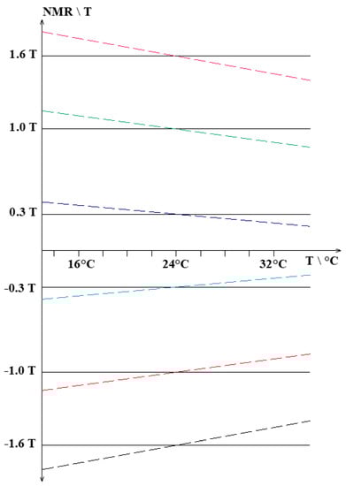
Figure 10.
Theoretical modelling plot of the instrument output response in comparison to the NMR output for a temperature sweep. Sensitivity response of the instrument output is explained through the varying slope value across the magnetic field range.
The NMR plot and the instrument output were expected to cross at the ambient reference temperature of 24 °C as the instrument output is compensated at this temperature through linearity calibration. The error plot in Figure 11 shows the magnetic field error for each plateau which is found when subtracting the magnetic field value given by the instrument from the NMR. These plots outline the individual slope values given by KMF and the y-intercept values given by CMF.
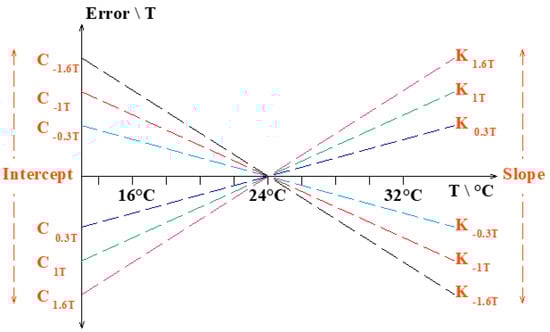
Figure 11.
Error plot extracted from Figure 10 when subtracting the instrument output response from the NMR reading. A set of slope values KMF and intercept values CMF is obtained.
Therefore, relating the slope values given by KMF and the y-intercept values given by CMF to the instrument magnetic field value outputs gives the relation plots as shown in Figure 12 and Figure 13.
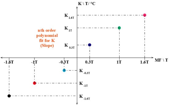
Figure 12.
Plot showing the theoretical relation that is obtained between the magnetic field values given by the instrument with respect to the slopes values of the error (KxT). This relation must be modelled using an nth order polynomial.
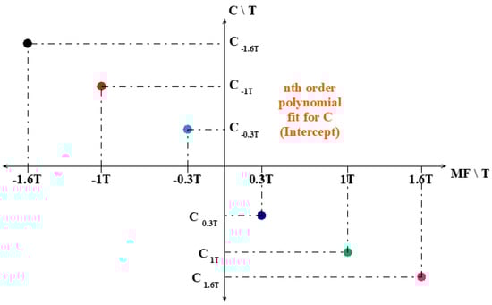
Figure 13.
Plot showing the theoretical relation that is obtained between the magnetic field values given by the instrument with respect to the intercept values of the error (CxT). This relation must be modelled using another nth order polynomial.
By applying the nth order polynomial fit from Figure 12 to the MF value given by the instrument we get the corresponding KxT value. By applying the nth order polynomial fit from Figure 13 to the MF value given by the instrument we get the corresponding CxT value. The values of KxT and CxT map directly on one of the error plots in Figure 11.
As the temperature value is given by the PT100 and KxT and CxT are now known, the error value from Figure 11 can be computed. This error is subtracted from the linearized compensated reading to get the “temperature sensitive” compensated reading. In conclusion, modelling temperature sensitivity requires two independent nth order polynomials for modelling the slope and intercept values respectively.
The application of this algorithm was applied to the real obtained data from the instrument and the NMR. Figure 14 shows the real response for the temperature sweep in the case for the 0.3 T reading. As the Peltier element heats up and cools down, the iron pole of the electromagnet in contact with the Peltier element also registers a change in temperature. The change in temperature results in a slight change in the magnetic field which is indicated by the NMR reading in green in Figure 14.
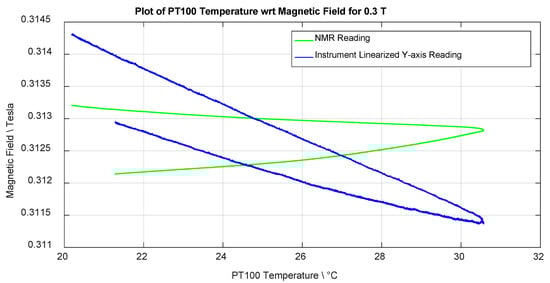
Figure 14.
Graph showing the response of both the NMR and the instrument as the Hall probe is subjected to a field of 0.3 T and its temperature varied from 20 °C up to 31 °C using a Peltier element.
An error plot for each of the six operating magnetic field points was extracted and are shown superimposed in Figure 15. As the reference ambient temperature was 24 °C, at which nonlinearity compensation is performed, the error plots in Figure 15 are supposed to cross each other with a null error at this temperature. However, limitations in the physical setup during the calibration procedure yielded such errors.
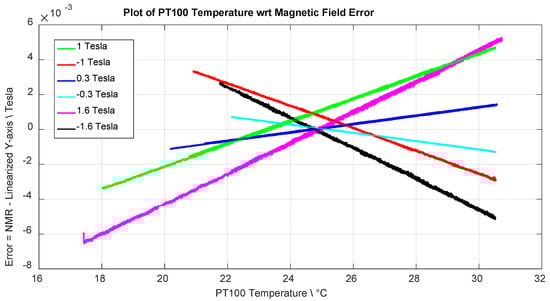
Figure 15.
Superposition of all the errors obtained for each of the 6 magnetic field plateaus tested.
As theoretically explained, the slope values plot shown in Figure 16 and the intercept values plot shown in Figure 17 are extracted from Figure 15. Linear and cubic polynomials are tested in modelling the relation in Figure 16 to see the error reduction upon application of the algorithm for each case attained using “Temperature Compensation of Sensitivity” after linearization was performed. The intercept relation in Figure 17 was only modelled using a linear fit.
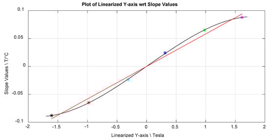
Figure 16.
Graph showing the slope values of the errors as in Figure 12 for each plateau. A cubic polynomial (black) is deemed best in characterizing all the slope values across the whole range in comparison to the linear polynomial fit (red).
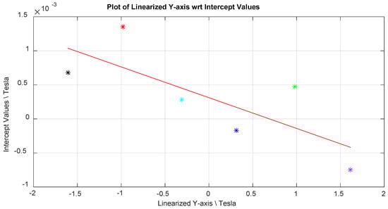
Figure 17.
Graph showing the intercept values of the errors as in Figure 13 for each plateau. A linear polynomial fit is deemed best in characterizing all the intercept values across the whole range.
Table 2 shows a breakdown of the mean percentage errors obtained upon the sequential application of nonlinearity compensation, offset compensation and temperature sensitivity compensation. A comparison is also made between the application of a third order polynomial and a first order polynomial in modelling the slope values from Figure 16 for temperature sensitivity.
Table 2.
% mean errors obtained at the different calibration steps for the six magnetic field plateaus tested.
5.2.4. Electronics Temperature Compensation
The effect of the temperature variation of the electronics on the magnetic field instrument reading is taken into consideration by the block “Electronics Temperature Compensation”.
In order to study this effect, the instrument was placed in a temperature chamber in which the temperature was swept from 17 °C up to 34 °C while the Hall Probe was placed in a zero gauss chamber at the ambient reference temperature of 24 °C. The electronics temperature was read using the on-board TMP112 high accuracy 12-bit digital temperature sensor which monitored precisely the analog electronics temperature. The linearized output from the instrument was plotted against the temperature of the instrument as shown in Figure 18. The 1st order polynomial extracted from Figure 18 was used to compensate for any changes in the offset when the electronics temperature drifted from the reference ambient temperature of 24 °C.
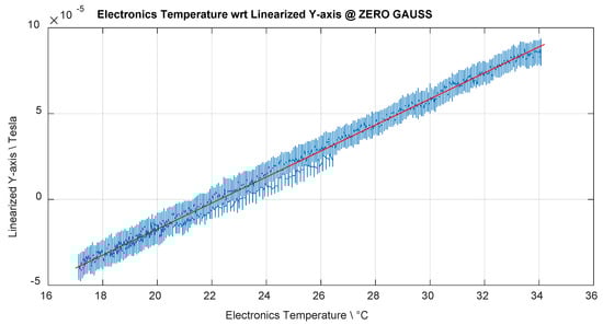
Figure 18.
Graph showing the variation of the instrument output when the Hall probe is at zero gauss and at ambient reference temperature while the electronics temperature is varied from 17 °C up to 34 °C. This additional offset is compensated for using a 1st order polynomial fit.
A major fallback of this test alone is that the offset shown can be only said to have this magnitude at zero gauss and not throughout the full magnetic dynamic range. In order to properly model the variation effect of the electronics temperature on magnetic field readings, a calibration block for “Electronics Temperature Compensation of Sensitivity” should be included in the calibration process. This test is not currently implemented and can be an additional improvement to the current calibration process. In this test the Hall probe should be subjected to different fields across the full range and for each field a temperature sweep of the electronics instrument is performed.
6. Calibration Verification
Calibration verification test runs were performed for all three axes covering the whole ±2 T full dynamic range at various temperatures.
Calibration result Table 3 summarizes the absolute percentage errors obtained for all axes of each instrument before and after calibration while Figure 19 shows graphically the improvement obtained for the Y-axis. Apart from a reduction in the mean error which effectively results in an offset of the true reading, one can also note that calibration decreases the spread in the error. Predominantly the mean error is reduced by the “Nonlinearity Compensation” block as shown in Figure 20 while the spread in the error is then reduced by “Temperature Compensation of Sensitivity” as shown in Figure 21 for the 0.3 T case. We see that as the temperature of the Hall probe is increased from 21 °C up to 31 °C from Figure 21, the instrument registers a positive percentage error increase which is reduced significantly when temperature sensitivity compensation is applied.
Table 3.
Tabulation of the reduction in percentage errors obtained for all axes upon calibration application.
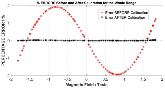
Figure 19.
Graph showing the reduction in the percentage error after calibration.
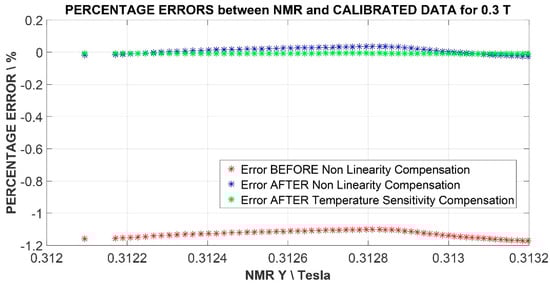
Figure 20.
Graph showing the offset reduction obtained for the case of 0.3 T by application of nonlinearity compensation.
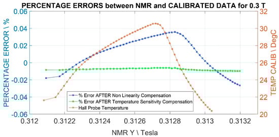
Figure 21.
Graph showing the additional improvement obtained in the percentage error spread by application of “Temperature Sensitivity Compensation” after “Non-Linearity Compensation” is applied when the Hall probe temperature is thermally cycled from 21 °C up to 31 °C.
7. Calibration of Angular Errors of the Hall Probe
The full calibration of a multi-axes Hall sensor should also include correction of angular errors of the Hall probe. Therefore the difficulty of performing very precise calibration of a three axes sensor is increased due to the presence of the mutual coupling between the axes.
As indicated in Reference [9] the Hall sensor dies cannot be glued to the probe substrate so as to be perfectly parallel with the reference plane and edges of the probe package. Over and above this, the sensitivity vectors of the sensor are not perfectly oriented with respect to the dice planes and edges. This results in angular errors in the range of 1° of the Hall probe sensitivity with respect to the probe package reference axes.
As explained in Reference [9] the calibration of the angular errors is carried out by inserting the Hall probe flat in a hollow cube like tool so that one component of the probe is perfectly aligned with the magnetic field component B. The Hall probe is rotated in 90° angle steps and in each position the instrument output is read. This is repeated for different magnetic fields and for all three axes. Data analysis is performed in order to determine the sensitivity vector S as in Equation (2) where B is the magnetic flux density vector and Vh is the Hall voltage vector given by the individual calibration of each axis. Equation (3) gives the expanded matrix notation of Equation (2).
8. Conclusions
Reference to the development of a high precision teslameter has been made with a detailed overview of the calibration involved. The calibration procedure involved the application of high order mathematical polynomials to precision measurement data in order to correctly model the nonlinearity and temperature sensitivity of the Hall probe. Nonlinearity is modelled using a 5th order polynomial registering a percentage error reduction in the peak error of around 1.903819% over the full ±2 T range. A reduction in the error spread over temperature is obtained upon application of temperature compensation of sensitivity using a 3rd order polynomial fit. A comparison of the results obtained in using different order polynomials in modelling both temperature and non-linearity effects has been highlighted thus outlining the importance of such experimentation. A full investigation of the improvements obtained through the application of the calibration of the angular errors still needs to be done and is considered as further work in this research project.
The presented calibration procedure has been designed, tested and fully verified on the developed instrumentation [7,8]. The determination of all the calibration coefficients for the different polynomial orders involves a great deal of data analysis and computational power. Tailored MATLAB scripts have been coded for the determination of the calibration parameters in order to speed up the data analysis process. The predominant parasitic effects of Hall probes as stated in Reference [1] are all being calibrated for and improvement on the technique as presented in Reference [2] is also reported. As [2] presents teslameter calibration based on an analog electronics module one can appreciate the limitations in both precision and accuracy obtained. A direct comparison can be made on the order of the polynomials used for the modelling of the Hall probe response. Predominantly in Reference [2] non-linearity compensation is implemented using a third order op-amp based circuit whereas in this presented study a fifth order polynomial has been proved to give much superior absolute accuracy in the final calibrated readings. The recent study [9] shows a different calibration approach taken where the Hall voltage is approximated by a polynomial function of 2nd degree that corresponds to the first ten terms of a Taylor series. While one can appreciate the relevance of such a mathematical computation it does not yield the individual improvement obtained in the calibration of each parasitic effect and thus remains very challenging in determining each optimal polynomial fit to be used.
As the 200 MHz on-board microcontroller of the instrument carries out all the calibration calculations for every acquired data point as explained throughout this article, a study has been conducted which quantifies the required clock cycles taken by the microcontroller to perform such calculations on a single data point. Tabulation of the results obtained is shown in Table 4.
Table 4.
Breakdown of all calibration steps in terms of the number of clock cycles on the TMS320F28379D 200 MHz microcontroller.
It is to be noted that the two most computation demanding calibration steps are “Non-Linearity Compensation” and “Temperature Compensation of Sensitivity” given that a fifth order polynomial needs to be computed for the former and the merging of a cubic fit and a linear fit must be done for the latter as explained in Section 5.2.3. From Table 4 it can be concluded that as the total number of clock cycles to perform a calibration of a single data point takes 88 clock cycles on the 200 MHz microcontroller this results in an overall duration of 0.44 μs.
Author Contributions
Formal analysis, J.C.; Investigation, J.C.; Methodology, J.C.; Software, J.C.; Supervision, A.S. and N.S.; Validation, A.S., N.S., M.C., Z.M. and R.S.P.; Writing—original draft, J.C.; Writing—review & editing, A.S., N.S., M.C. All authors have read and agreed to the published version of the manuscript.
Funding
This research received no external funding.
Acknowledgments
The authors would like to thank Sasa Spasic, Marjan Blagojevic and their team at Sentronis in Niš, Serbia, for their support during the calibration of the developed instrument.
Conflicts of Interest
The authors declare no conflict of interest.
References
- Sanfilippo, S. Hall probes: Physics and application to magnetometry. In Presented at the Specialised Course on Magnets; Paul Scherrer Institut: Villigen, Switzerland, 2009; pp. 423–462. [Google Scholar]
- Popovic, D.R.; Dimitrijevic, S.; Blagojevic, M.; Kejik, P.; Schurig, E.; Popovic, R.S. Three-Axis Teslameter With Integrated Hall Probe. IEEE Trans. Instrum. Meas. 2007, 56, 1396–1402. [Google Scholar] [CrossRef]
- Popovic, R.S. High Resolution Hall Magnetic Sensors. In Proceedings of the 29th International Conference on Microelectronics, Belgrade, Serbia, 12–14 May 2014; pp. 69–74. [Google Scholar]
- Popovic, R.S. Hall Effect Devices, 2nd ed.; IOP Publishing: Philadelphia, PA, USA, 2004; Chapters 4 and 5. [Google Scholar]
- Mosser, V.; Matringe, N.; Haddab, Y. A Spinning Current Circuit for Hall Measurements down to the Nanotesla Range. IEEE Trans. Instrum. Meas. 2017, 66, 637–650. [Google Scholar] [CrossRef]
- Junfeng, J.; Wilko, K.; Kofi, M. A Continuous-Time Ripple Reduction Technique for Spinning-Current Hall Sensors. IEEE J. Solid-State Circuits 2014, 49, 1525–1534. [Google Scholar]
- Cassar, J.; Sammut, A.; Sammut, N.; Calvi, M.; Dimitrijevic, S.; Popovic, R.S. Design and Development of a Reduced Form-Factor High Accuracy Three-Axis Teslameter. J. Electron. 2019, 8, 368. [Google Scholar] [CrossRef]
- Cassar, J.; Sammut, A.; Sammut, N.; Calvi, M.; Spasic, S.; Renella, D.P. Performance Analysis of a Reduced Form-Factor High Accuracy Three-Axis Teslameter. J. Electron. 2019, 8, 1230. [Google Scholar] [CrossRef]
- Popovic, D.R.; Dimitrijevic, S.; Spasic, S.; Popovic, R.S. High-accuracy teslameter with thin high-resolution three-axis Hall probe. J. Int. Meas. Confed. 2015, 98, 407–413. [Google Scholar] [CrossRef]


© 2020 by the authors. Licensee MDPI, Basel, Switzerland. This article is an open access article distributed under the terms and conditions of the Creative Commons Attribution (CC BY) license (http://creativecommons.org/licenses/by/4.0/).