Article

CENNA: Cost-Effective Neural Network Accelerator

Department of Electronics and Computer Engineering, Hanyang University, Seoul 04736, Korea
*
Author to whom correspondence should be addressed.
Electronics 2020, 9(1), 134; https://doi.org/10.3390/electronics9010134
Submission received: 23 December 2019 / Revised: 6 January 2020 / Accepted: 8 January 2020 / Published: 10 January 2020
(This article belongs to the Special Issue Hardware and Architecture Ⅱ)

Abstract

:
Convolutional neural networks (CNNs) are widely adopted in various applications. State-of-the-art CNN models deliver excellent classification performance, but they require a large amount of computation and data exchange because they typically employ many processing layers. Among these processing layers, convolution layers, which carry out many multiplications and additions, account for a major portion of computation and memory access. Therefore, reducing the amount of computation and memory access is the key for high-performance CNNs. In this study, we propose a cost-effective neural network accelerator, named CENNA, whose hardware cost is reduced by employing a cost-centric matrix multiplication that employs both Strassen’s multiplication and a naïve multiplication. Furthermore, the convolution method using the proposed matrix multiplication can minimize data movement by reusing both the feature map and the convolution kernel without any additional control logic. In terms of throughput, power consumption, and silicon area, the efficiency of CENNA is up to 88 times higher than that of conventional designs for the CNN inference.

1. Introduction

Convolutional neural networks (CNNs) have emerged as a key technology for machine learning. They have proven to be a powerful tool for computer vision applications ranging from image recognition of handwritten digits to complex object recognition [1,2,3]. In addition, they have made tremendous progress in various applications including audio/speech recognition and natural language processing [4,5,6].
Recently, state-of-the-art CNN models have exhibited superior classification performance over humans, but they require a considerable amount of computation and a large amount of memory space because they typically employ many processing layers. Specifically, convolution layers account for over 90% of the overall computation workload in CNNs [7]. Convolution layers perform a significant amount of element-wise multiplications and additions between input feature maps and convolution kernels to generate output feature maps. However, processing in a convolution layer is adequate for parallel computation and is commonly accelerated using graphic-processing units (GPUs). A GPU can accelerate CNNs quickly, but in a battery-powered embedded system, relying heavily on GPUs may lead to an unacceptably large amount of energy dissipation [8].
Numerous studies have attempted to expedite the processing speed and improve energy efficiency by designing hardware accelerators for CNNs [9,10,11,12,13]. In particular, these studies have great significance for attempting CNN in a low power edge computing environment. However, many unsolved issues remain. One of them is the hardware cost. In a convolution layer, a large number of multiplication operations between feature maps and convolution kernels are required. It is also important to exploit parallelism in a hardware accelerator in CNN. Most CNN accelerators can support the parallelism by designing either an array structure of processing elements (PEs) or a parallel tree reduction structure [9,10,11,12,13]. To maximize the performance through parallel processing, most implementations employ many computation units including multipliers and adders. In particular, employing many multipliers may lead to excessive circuit size and unacceptably large energy consumption. Another key issue is how to manage data efficiently when multiple operations are being conducted in parallel. Therefore, critical issues such as data reuse and data synchronization need to be solved. Specifically in CNN, both feature maps and convolution kernels are heavily reused in the processing in convolution layers. Therefore, data reuse is important for reducing data movement between an accelerator and off-chip memory. However, many existing implementations [9,12] suffer from heavy power consumption because complicated computation and control circuits for data reuse are employed. This prompts the need for a specialized accelerator to achieve higher performance at lower hardware cost.
In this study, we propose a cost-effective neural accelerator named CENNA. We propose a cost-centric matrix multiplication method to reduce the hardware cost. The proposed method is implemented in the hardware. We verified that it is possible to reduce the hardware cost without degrading computation performance. Furthermore, a novel convolution method that minimizes data movement by reusing both the feature map and the convolution kernel without any additional control is proposed. Therefore, the proposed implementation achieves reasonable silicon area, low power consumption, and good performance and it can be used for edge computing applications such as drones, autonomous vehicles, and on-device artificial intelligence (AI) [14,15,16].
The rest of this paper is organized as follows. Section 2 introduces CNN and presents some challenges in the implementation of CNN accelerators. Section 3 presents the proposed matrix multiplication engine, the architecture of CENNA, and along with the data reuse method in CENNA. Section 4 presents the experimental results. The performance, hardware size, and power consumption of CENNA are compared with those of state-of-the-art designs in Section 5. Finally, this study ends with concluding remarks in Section 6.

2. Background and Related Works

In this section, we first introduce the basic features of CNN. Then, we discuss the key issues involved in designing CNN accelerators from two perspectives: computational complexity and data reuse.

2.1. Convolutional Neural Network (CNN)

CNNs are a set of pattern recognition filters that can be learned by training [1]. Most CNNs consist of multiple layers that include convolution layers, non-linear operation layers, sub-sampling layers, and fully connected layers. These layers are arranged in a feed-forward structure. Typically, the group of convolution layers and sub-sampling layers performs feature extraction and the group of fully connected layers performs classification. Through the process of each layer, feature maps that represent various features of an input image can be extracted. Image features include lines, corners, and edges, etc. Classification is carried out based on the extracted features.
The convolution layer is an essential process in CNN, and it carries out element-wise multiplications between images and filters. Figure 1a presents the set of computations in a convolution layer. The convolution layer receives a D-channel input feature map as an input image. Each input feature map is convolved with K × K × D kernels by shifting the kernel window to generate one pixel in a Z × Z output feature map. The stride of the receptive field is S, and T output features will form the set of input feature maps for the next convolution layer. After output features are generated, they are filtered using an activation function such as sigmoid, tanh, and rectified linear unit (ReLU). Figure 1b shows a pseudo code that describes operations that are carried out in a convolution layer where element-wise multiplications between an input feature map (inFmap) and a convolution kernel (cKernel) are performed to extract features and generate an output feature map (outFmap).
Following the convolution layer, the sub-sampling layer reduces the size of feature from the previous layer. This layer is frequently used in a CNN to gradually reduce the spatial size of the features and the computational complexity of the network by reducing several adjacent neurons in a feature map. After feature extraction with multiple convolution and sub-sampling layers, the fully connected layer follows. The term “fully connected” indicates that all neurons in the current layer are connected to all neurons in the next layer. The output feature map from convolution and sub-sampling layers represents high-level features of the input image. In contrast, the output of the fully connected layer is the classification result.

2.2. Key Issues in CNN Accelerator Implementation

Convolution layers require a large amount of computations and data transfer from and to the off-chip memory. We shall discuss these issues as key challenges in the implementation of CNN accelerators.

2.2.1. Computation Complexity

Today, state-of-the-art CNN models can recognize objects with more accuracy than human recognition [17,18]. The exceptional accuracy of the CNN is primarily achieved through deep convolution layers, but each convolution layer requires a large number of multiplications and additions. For instance, ResNet-152 [18] requires 11 G multiply-accumulate (MAC) operations as shown in Table 1.
To perform a large amount of MAC operations, CNN hardware accelerators in [9,10,11,12,13] employed numerous multipliers and adders. There are two types of architecture: a PE array structure and a reduction tree structure as shown in Figure 2.
Figure 2a shows a typical PE-array structure. It consists of a buffer called a global buffer, a first-in first-out buffer (FIFO), and arrays of PEs (PE array). Each PE consists of a multiplier and an adder. In the PE-array structure, typically, a buffer called Global Buffer loads the data from an off-chip dynamic random-access memory (DRAM). The loaded data is sent to FIFO that distributes the data to the PE array. The multiplication between the feature map and the convolution kernel can be executed in parallel if numerous PEs are available. Therefore, implementations in [9,10,11] employ many PEs to achieve highly parallel computation.
Figure 2b show a typical reduction tree structure. In this structure, multiplications and additions are executed in parallel and the weighted results are combined into one, which is called a reduction operation. It consists of a Reduction Tree (including multipliers and adders), a buffer for distributing input values (Distributor), and a Prefetch Buffer. As in the PE array structure, data are loaded from the off-chip DRAM and stored in the prefetch buffer. The distribution buffer takes data from the prefetch buffer and distributes input values to multipliers. To fully utilize the parallelism in this structure, numerous multipliers and a large reduction tree are required [12,13].
Multiplication is a much more computationally costly operation than addition [20,21]. As shown in Table 2, the energy consumed by a multiplier is up to 6.7 times more than that consumed by an adder. In addition, the multiplier requires 7.8 times more silicon area. Therefore, for a convolution layer, in which many multiplications are performed, a lot of energy dissipation and silicon-area are required. Hence, in the matrix multiplications, where numerous multiplications are performed, converting multiplication to additions is effective in reducing the cost.
Prior studies on reducing the amount of multiplications were based on either Strassen’s multiplication or Winograd’s multiplication [7,22]. A computational complexity of O(n3) in naïve multiplication is reduced to O(n2.807) in Strassen’s multiplication and O(n2.795) in Winograd’s multiplication. For example, to perform a 2 × 2 matrix multiplication, naïve multiplication requires eight multiplications, but both Strassen’s method and Winograd’s method require seven multiplications [20]. The number of multiply operations is reduced in Strassen’s and Winograd’s method. However, the number of add/sub operations and the number of computation steps in a matrix multiplication increase. This means that more complicated add/sub logic circuits and more memory transactions to store and retrieve intermediate results are needed.
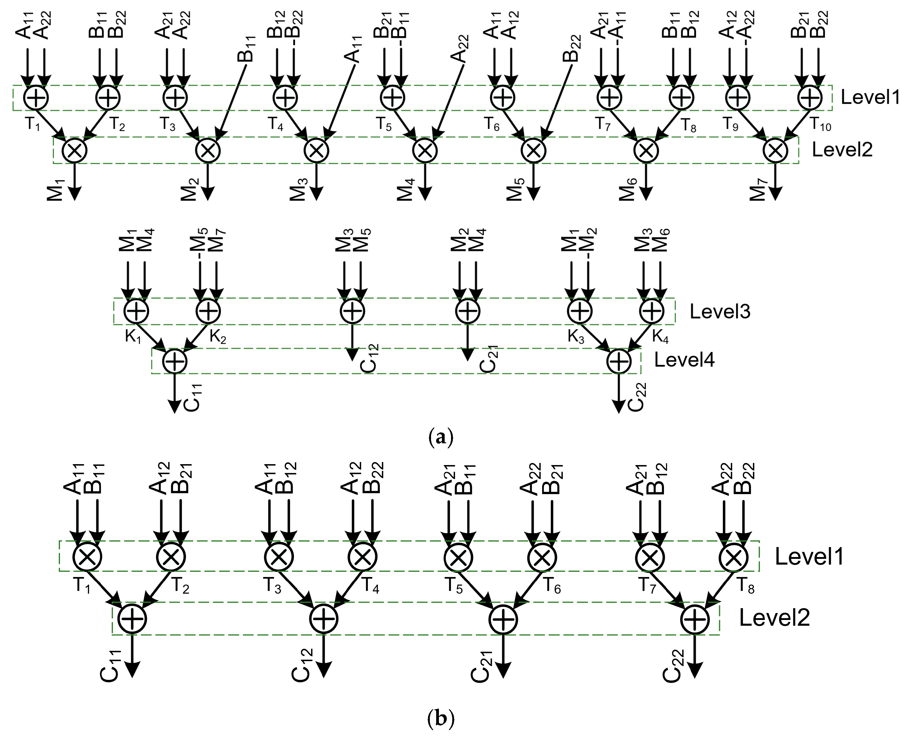
In the case of Strassen’s multiplication of two 2 × 2 matrices, the computation step required to obtain each element of the result matrix is different whereas the arithmetic steps to compute each element in naïve multiplication are uniform [23]. For instance, as shown in Figure 3a and Figure 4a, in the multiplication of two 2 × 2 matrices to get C11, C12, C21 and C22, computing C11 requires four arithmetic steps, whereas computing C12 requires three steps. However, as shown in Figure 3b and Figure 4b, in naïve multiplication, each result requires the same four arithmetic steps. The more the arithmetic steps, the more memory they require, which leads to additional power consumption. Furthermore, the larger the matrix size, the more irregular the arithmetic steps become. For example, to calculate a 4 × 4 Strassen’s multiplication, the total number of arithmetic steps is eight, and it requires six to eight steps depending on elements in the final product matrix. In contrast, the naïve multiplication requires only the same three steps for every element in the final result. This means that, as the size of the matrix increases, Strassen’s multiplication requires more memory than naïve multiplication, and the steps involved in computing the result shall become more irregular. The performance and the hardware cost of a pipelined implementation are approximately determined by how appropriately pipeline stages are divided [24,25]. In addition, if the delay in each pipeline is uneven, such irregularity causes a significant complexity increase and energy inefficiency [26]. Thus, it is not straightforward to determine the pipeline stages and the balanced delay of each pipeline stage because of the irregular arithmetic steps.

2.2.2. Data Reuse

As presented in Table 1, most CNN models require a large number of kernel parameters. For example, VGG-16 [27] requires 528 MB to store all the kernel parameters. Furthermore, the cost to access an off-chip memory (DRAM) is over 200 times more expensive than the multiplication cost in terms of energy dissipation [21]. In a convolution layer, pixels in an input feature map are repeatedly used for convolution operations with many convolution kernels. In addition, as a kernel window slides through an input feature map, some values of the feature map are reused consecutively. Therefore, it is important to bring the convolution kernel and the input feature map from the off-chip memory to the on-chip memory and to reuse them as much as possible.
Most CNN accelerators commonly employ a large array of PEs to carry out highly parallel computing. In such a structure, values loaded from an off-chip memory are stored in an on-chip memory, typically called a Global Buffer, and this buffer is shared among PEs to avoid large amounts of data transfers from the off-chip memory. As shown in Figure 2a, each PE exchanges data with other PEs via a bus and each is connected to the off-chip memory controller (Memory Controller, MC). Each PE includes not only the logic circuits for computation but also a controller to communicate with other PEs. In the communication between PEs, each PE sends and receives the data of a feature map and a convolution kernel. If the communication between PEs becomes complex, the hardware cost increases. The implementation cost of the PE-array-based method is typically very high [9,11]. The implementation in [9] shows that more than half of the power consumption is derived from hardware logic blocks for data reuse.
In a reduction-tree based accelerator, data distribution logic blocks (Communicator and Distributor) are utilized for data reuse. To reduce the data movement from DRAM, this architecture typically stores reused data to a prefetch buffer (Prefetch Buffer) and distributes it to a reduction tree (Reduction Tree) using distribution logic circuits, as shown in Figure 2b. The reduction tree has a fixed data flow that performs multiplications in parallel and accumulates the results of the multiplications into an accumulator. In a fixed flow, data reuse is employed using a communicator logic circuit (Communicator) that allows data reuse between multipliers, as shown in Figure 2b. Implementations in [10,11] employed a logic block for data sharing between multipliers to enable flexible data sharing, but heavy power consumption and silicon area were observed.
The distribution logic block (Distributor) provides both the feature map data and the convolution kernel data to multipliers. This makes it possible to reuse data either using a single feature map with multiple kernels or using multiple feature maps with a single kernel. Therefore, the distributor logic holds a lot of data, which leads to high power consumption and large silicon area. In addition, the implementation employs two reuse schemes (Communicator and Distributor), and it suffers from excessive power consumption and large chip area [12].

3. Cost-Effective Neural Network Accelerator (CENNA) Architecture

This section describes the structure of CENNA and how CNN works in CENNA. In CENNA, the convolution operation is converted to a form of 4 × 4 matrix multiplication as a pre-processing step. It will be addressed that the conversion to a 4 × 4 matrix multiplication is advantageous for low hardware cost and reusing data. We will discuss a matrix multiplication engine in terms of hardware cost and explain how to compute a convolution operation using the matrix multiplication. In addition, we describe a novel method for data reuse.

3.1. Proposed Matrix Multiplication Engine

As mentioned in Section 2.2.1, a multiplier is much more complicated than an adder. Therefore, reducing the number of multiplications in a matrix multiplication will be effective to reduce the hardware implementation cost. To compare the implementation cost of a multiplier for matrix multiplications, three methods that perform a 4 × 4 matrix multiplication are implemented: a naïve multiplication, a Strassen’s multiplication, and the proposed cost-centric matrix multiplication.
For multiplication of two 4 × 4 matrices, while the naïve multiplication requires 64 multiplications, Strassen’s multiplication requires only 49 multiplications. However, although the number of multiplication operations in Strassen’s method is significantly smaller, as shown in Table 3, the actual hardware cost is similar. The main reason is that Strassen’s method requires more memory and adder/subtractors to carry out more arithmetic steps than naïve multiplication. Furthermore, the multiplier for Strassen’s method is slower than the naïve multiplier because of complex steps in Strassen’s multiplication. In addition, because of the irregular steps of Strassen’s multiplication, designing a pipelined implementation will be more difficult.
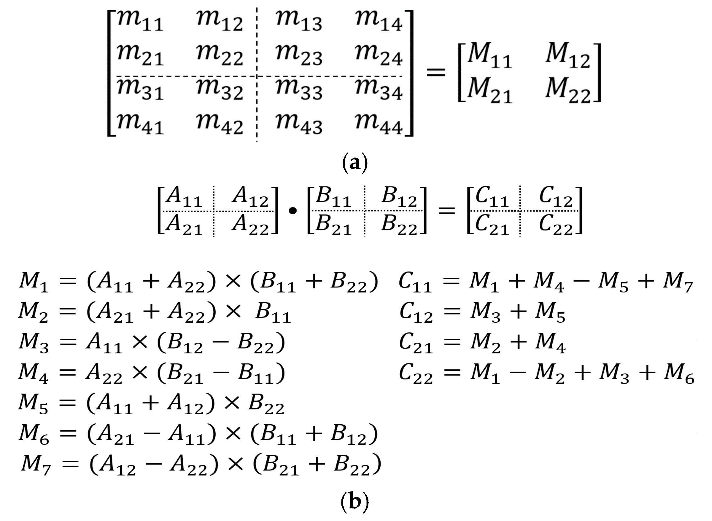
In CENNA, a new matrix multiplication called cost-centric multiplication is proposed. Cost-centric multiplication employs a hybrid method that is a combination of Strassen’s method and the naïve multiplication. In the cost-centric multiplication, the input 4 × 4 square matrix is partitioned into four 2 × 2 sub-matrices as shown in Figure 5a. In cost-centric multiplication, the naïve matrix multiplication and addition are employed to compute seven 2 × 2 intermediate result matrices (M1M7), and those seven sub-matrices are added and subtracted in the same way as Strassen’s method as shown in Figure 5b. The cost-centric multiplication operates in three arithmetic steps: (i) summation and difference of 2 × 2 sub-matrices (e.g., A11 + A22, B12B22), (ii) the naïve multiplication of the summations and differences to obtain M1M7, and (iii) summations and differences of some Mi’s to compute the result (C11, C12, C21, and C22).
The proposed method requires 56 multiplications, which is more than the original Strassen’s multiplication. However, the power consumption of the proposed matrix multiplication is less by 17% than that of the original Strassen’s multiplication as shown in Table 3. The proposed method dissipates less power than the implementation of the naïve method and Strassen’s method, respectively. In addition, the operating frequency of the pipelined implementation of the proposed method is higher than that of the implementation of Strassen’s multiplication. In Strassen’s multiplication, arithmetic steps required to obtain each value in the result matrix are not regular. Thus, designing evenly balanced pipeline implementation is difficult.
The operating frequency of the pipelined implementation of the proposed matrix multiplication is the same as that of the naïve multiplier at 500 MHz. In contrast, the proposed matrix multiplication dissipates less power than the naïve implementation. It dissipates smaller power than the other two multipliers compared, and it can operate at the same frequency as the naïve matrix multiplication, which is faster than Strassen’s matrix multiplier.
In conclusion, CENNA is designed to compute a 4 × 4 matrix using 2 × 2 matrices. The 4 × 4 matrix has advantages of accelerating the targeted neural network, details of which will be discussed in Section 3.3, Section 3.4 and Section 3.5. However, for the acceleration of a neural network that involves more computation, it requires a larger matrix computation. In order to address computation of large matrix multiplication, CENNA employs divide and conquer algorithm, which divides a problem into smaller subproblems and solve the subproblems recursively [28]. In CENNA, the large size matrix can be divided into sub-matrices until it cannot be decomposed by a 4 × 4 matrix and combines the sub-matrices to generate a solution to the large matrix.

3.2. CENNA Architecture

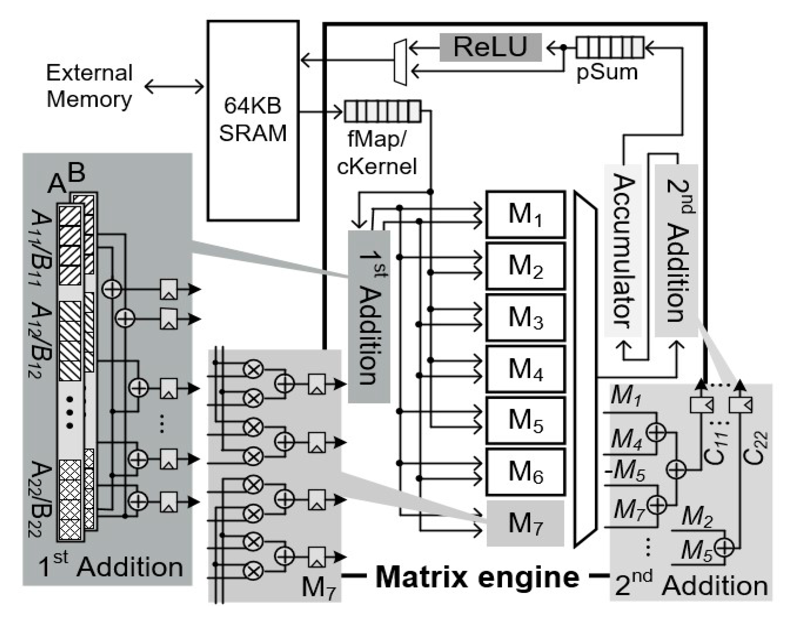
Figure 6 shows the hardware structure of CENNA. CENNA consists of a memory block (64 KB static random-access memory, SRAM) and the proposed matrix multiplier (Matrix Engine). The memory block stores convolution kernels and feature maps. Data from the external DRAM are stored in the memory block and are sent to Matrix Engine. The Matrix Engine consists of components for the proposed matrix multiplication (1st Addition, M1M7, 2nd Addition) and those for convolution operations (fMap, cKernel, Accumulator, ReLU, and pSum).
As mentioned earlier, the proposed multiplier operates in 3 steps. The 1st Addition unit carries out the first step, which involves the summation and difference of the 2 × 2 sub-matrices (e.g., A11 + A22 and B12B22). Each M unit in Figure 6 carries out naïve multiplication of summations and differences of results from the 1st Addition to obtain M1M7, and the 2nd Addition unit carries out summations and differences of some of the Mi’s to compute the results (C11, C12, C21 and C22). Each M unit contains 8 multipliers and 4 adders. Because CENNA includes 7 M units (M1M7), a total of 56 multipliers operate in parallel.
The fMap buffer and the cKernel buffer store a portion of the feature map and the convolution kernel. We have provided a detailed description on fMap and cKernel in Section 3.3. The Accumulator unit accumulates the result of matrix multiplication to obtain an output feature map of CNN. The pSum buffer stores the result of the Accumulator unit and the result is passed to either the ReLU unit or the memory block depending on whether an output feature map is completely computed. The ReLU unit performs the rectifier linear unit (ReLU) function. When an output feature map is completely generated, the values will go through the ReLU unit, and eventually will be stored in the 64K SRAM block.

3.3. Convolution Operation in CENNA

This CENNA architecture employs not only a cost-efficient matrix multiplication engine, but also an efficient data reuse technique for the 4 × 4 matrix multiplication to reuse both convolution kernels and feature maps.
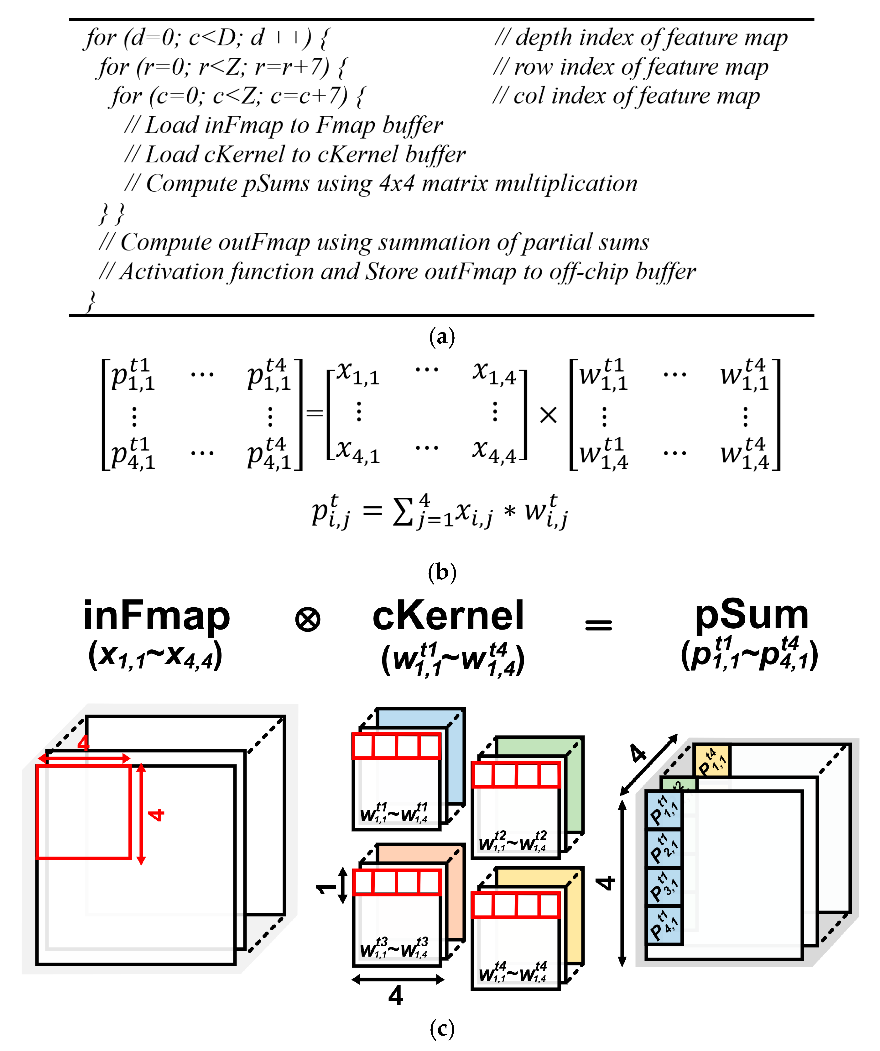
Figure 7a shows a pseudo code of the convolution operation in CENNA. First, it loads the feature map and the convolution kernel into buffers (fMap, cKernel). While loading data, the feature map and the convolution kernel are stored in a 7 × 7 size and in four types of convolution kernls in a 4 × 1 size in buffers. In CENNA, the kernel window moves along the 7 × 7 input feature map stored in the buffer. We will discuss the loading process detail in Section 3.4. Second, once data are loaded, matrix multiplication of a 4 × 4 size is performed. In the matrix multiplication between a feature map and a convolution kernel, the result of the matrix multiplication is a partial sum of the output feature map. Third, partial sums are combined to achieve an output feature map. Next, it is stored in the off-chip memory (External Memory) via the activation function.

3.4. Convolution Operation Using Matrix Mulitplication

Figure 7b,c show the set of key operations in CENNA. The result of matrix multiplication is obtained by multiplying an input feature map of 4 × 4 (xi,j) and four types of convolution kernels of size 4 × 1 (wti,j–wti,j+3), where i, j, and t indicate the row position, the column position, and the kernel type, respectively. In the first computation, the result (pt11,1) is a partial sum of the output feature map that pertains to the first row in the input feature map (x1,1–x1,4) and the first type of convolution kernel (wt11,1–wt11,4). The second computation (pt21,1) is a partial sum of the output feature map pertaining to the first row in the input feature map (x1,1–x1,4) and the second type of convolution kernel (wt21,1–wt21,4), etc. The computation between the second row in the input feature map (x2,1–x2,4) and the first type of convolution kernel (wt11,1–wt11,4) generates a partial sum (pt12,1) that is the convolution operation when the kernel window moves to the second row of the feature map. The same process is repeated, and partial sums are thus generated (pt11,1pt44,1).
After matrix multiplication of the input feature map of 4 × 4 (x1,1–x4,4) and the component of the first row of the convolution kernels (wt1,1–wt1,4), the input feature map when the kernel window is moved down by one row (x2,1–x5,4) is multiplied by values corresponding to the second row of the convolution kernels (wt2,1–wt2,4). Similarly, the remaining partial sums are calculated in the same way, as shown in Figure 8. Finally, all partial sums are combined to generate output feature maps.
CENNA architecture is optimized for both computing performance and data reuse. First, when partial sums of an output feature map are generated from convolutions of an input feature map and convolution kernels, it is desirable to reuse the feature map for parallel convolution operations with multiple convolution kernels. Specifically, the convolution operation between one row in the feature map and four types of convolution kernels can be parallelized. In addition, values for the four convolution kernels can be reused when conducting parallel convolution operations with four lines in a feature map. Second, as a convolution kernel moves along an input feature, at each intersecting location, convolution operations are carried out. Therefore, some values of a feature map can be used for convolution operations with both the kernel of the previous location and that of the current location. Multiplications between convolution kernel (wt1i,j–wt1i,j+3) and four rows in an input feature map (xi,j–xi+3,j+3) reuse such values. That is, the results of matrix multiplication (pt11,1pt14,1) are computed when one convolution kernel moves to the next row of an input feature map. In addition, it can be conducted in parallel.

3.5. Tiling-Based Data Reorganization

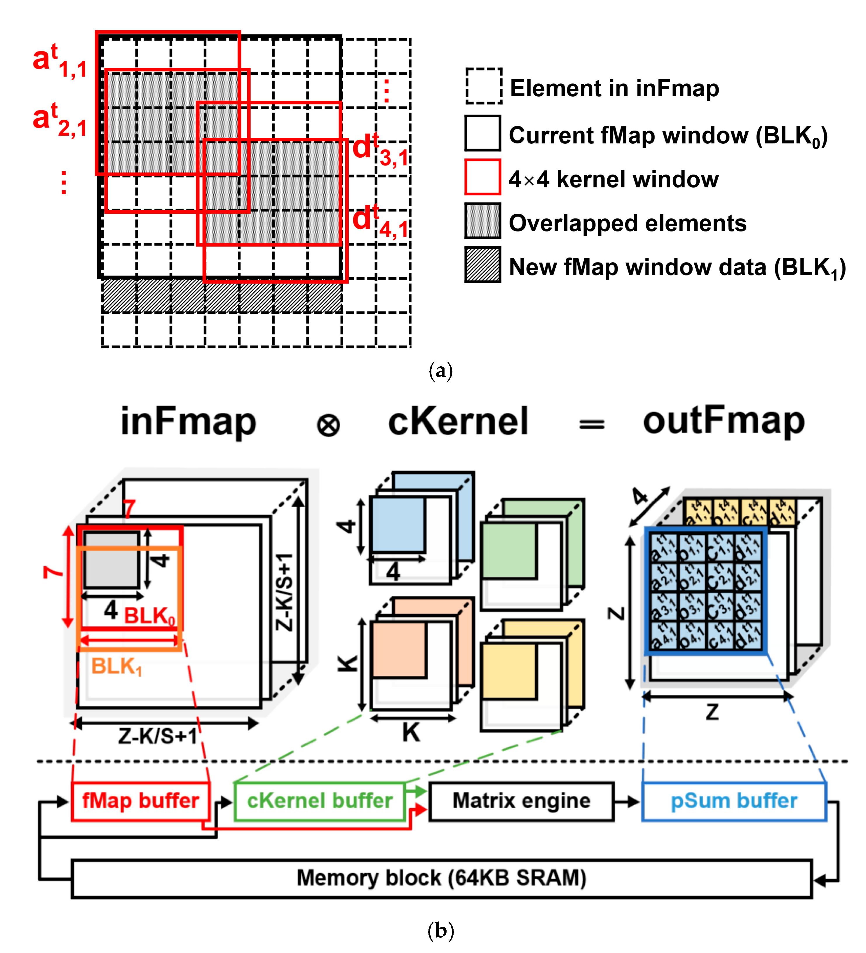
For efficient data reuse, a tile-based data reorganization method called data tiling (DT) is proposed in CENNA. The proposed tile-based data management partitions an input feature map into tiles of size 7 × 7 and a convolution kernel into four tiles of size 4 × 4, respectively. This approach simplifies dataflow and reduces hardware implementation complexity by accessing data to the on-chip memory with a uniform size. To implement the proposed DT method, CENNA employs an on-chip memory hierarchy that processes feature maps with several stages.
In the convolution layer, adjacent kernel windows have many overlapped elements. As shown in Figure 9a, two 4 × 4 size adjacent kernel windows (at1,1 and at2,1) have 12 overlapped elements in the feature map. Notably, most overlapped elements can be reused for the next kernel window if we reorganize overlapped elements to be adjacent. As shown in Figure 9b, a 7 × 7 tiled block of an input feature map (BLK0) is stored in the fMap buffer, and four types of 4 × 4 tiled convolution kernels are stored in the cKernel buffer. Next, a 4 × 4 kernel window in the fMap buffer moves across the current fMap window (BLK0) and generates partial sums, which will be stored in the pSum buffer. Through DT, the overlapped elements between adjacent 4×4 kernel windows can be reused when generating an output feature map (at1,1, at2,1 and dt3,1, dt4,1) as depicted in Figure 9b. In addition, for a new 7 × 7 tiled block of an input feature map (BLK1) operation, only the newly needed data are loaded.
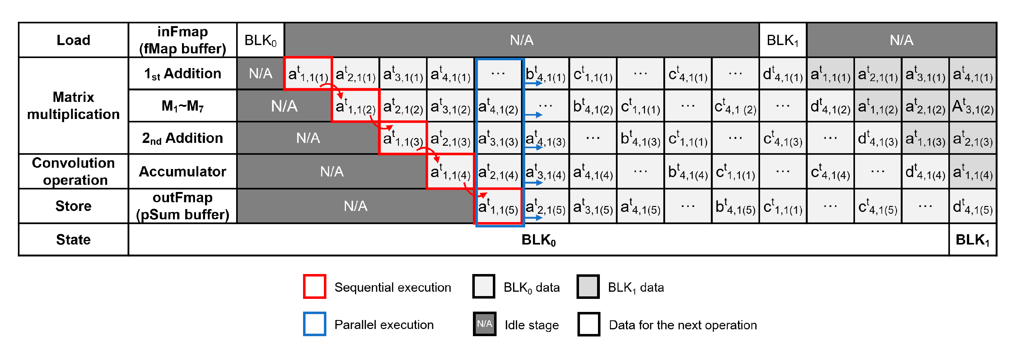
Figure 10 shows the pipelined execution flow in CENNA. The entire pipeline consists of four stages-Load, Matrix Multiplication, Convolution Operation, and Store stages. As explained in Section 3.1, the Matrix Multiplication stage is further divided into 3 stages, which makes the entire pipeline regarded as a 6-stage pipeline. During the Load stage, a 7 × 7 tiled block (e.g., BLK0) of an input feature map is fetched. In the Matrix Multiplication and Convolution Operation stages, CENNA carries out the convolution operation with the loaded 7 × 7 tiled block. The computed results (at1,1(4)) are stored in the pSum buffer during the Store stage. Eventually, after repeatedly processing all the tiled blocks, the final result (at1,1(5)) is obtained through the ReLU operation. It should be noted that when the pipeline is fully filled, five elements in the output feature maps are computed in parallel with only one set of execution units.

4. Hardware Implementation

The register transfer level (RTL) design of CENNA is implemented using Verilog hardware description language (HDL). The design is synthesized by Synopsys Design Compiler Ultra with Samsung 65 nm LP libraries under the worst-case operating conditions (1.08 V, 125 °C). The 64 KB SRAM is organized as eight banks of 512 × 128 b SRAMs. The energy dissipation of CENNA is estimated by Synopsys Power Compiler. In addition, CACTI v7.0 was used to estimate the amount of SRAM power consumption and area at 65 nm technology [29]. We implemented neural network accelerators that include three matrix multiplication methods: Naïve, Strassen, and CENNA. The results are summarized in Table 4.
Figure 11 shows the area and power consumption in each accelerator. Area and power consumption mainly incurred by the matrix multiplication are different from one another, whereas the cost of other parts is similar. As shown in Table 4, the Strassen implementation has the smallest silicon area among all compared implementations mainly because the circuit size for matrix multiplication is the smallest, as shown in Figure 11a. Compared to the Strassen implementation, CENNA implementation exhibits a 3% bigger silicon area. However, it consumes the smallest amount of power among all three implementations as shown in Figure 11b. The main reason why CENNA implementation dissipates the least amount of power is that the size of the local buffer is the smallest among all three. As shown in Table 4, the implementation for the Strassen requires more registers than other implementations. Therefore, it is possible to reduce the area by reducing the number of multipliers, but it consumes more power as the use of registers increases.

5. Evaluation

Because neural network accelerators are quite different from one another, it is difficult to compare CENNA to other architectures fairly. Therefore, in this study, accelerators are compared in various metrics. In CENNA, VGG-16 with a kernel of size 4 × 4 is used as a benchmark [30,31], and its basic configuration information such as the number of layers and types of filters is summarized in Table 5. To evaluate the performance of CENNA, we compare two types of neural network accelerators: the PE-array based [9,10,11] and the reduction tree-based [12,13].
In this section, we first explain the computing performance of CENNA when accelerating neural networks. Next, we compare CENNA with state-of-the-art accelerators in terms of performance, throughput, and hardware cost. Finally, we address the overall efficiency of CENNA and state-of-the-art accelerators.

5.1. Latency and Throughput of CENNA

Table 5 shows the average inference time of VGG-16 with 13 convolution layers when using CENNA, and it achieves 1.38 frame/s with an energy dissipation of 34.24 mJ on average. The total inference time includes the time for computation and memory access. The total inference time depends on the amount of MAC operations and the number of parameters. It depends on the shape of the feature map and convolution kernel. For example, Conv3-2 requires more computation than Conv1-2, but takes less time than Conv1-2. This is mainly because earlier layers require less output channels than later layers. Conv1-2 is a shallow output layer compared to Conv3-2 and the feature map cannot be reused as much as in Conv3-2.
We compare the inference performance of CENNA with other implementations, as shown in Table 6. The real throughput is estimated at 77% of the peak throughput, which is about 12% higher than that of the Strassen implementation. In the case of Conv1-1 layer of VGG-16, CENNA is 1.58 times faster than Strassen implementation. Furthermore, CENNA shows 1.68 and 1.06 times better efficiency than Strassen and Naïve implementations respectively, where the performance efficiency is real throughput per watt.

5.2. Performance Comparison with the State-of-the-Art Accelerators

The proposed neural network accelerator, CENNA, is compared with other existing works with respect to design metrics. Because of numerous differences in the structure and dataflow, it is difficult to compare the performance of CENNA and those of other implementations fairly. Therefore, we compared each implementation when each implementation is operating at real throughput and peak throughput. In addition, we compared the frame rate (frame/s) when the accelerator is running at real throughput.

5.2.1. Processing Elements (PE) Array-Based Accelerators

The PE-array based accelerator is classified by the communication method between PEs. We compared CENNA and three accelerators using the most representative communication methods (row stationary, 2D-SIMD, and 1D chain). Energy-Efficient Reconfigurable Accelerator for Deep Convolutional Neural Networks (Eyeriss) [9] is a well-known PE-array accelerator, which offers an efficient dataflow model called row stationary. Row stationary is a way to increase the reusability of data. It is designed to maximize data reusability inside a PE. As shown in Table 7, Eyeriss consumes 4.99 times more power and takes 8.88 times larger silicon area than CENNA. More than 45% of power consumption is in the PE network block such as the clock network and the PE controller circuit. In terms of peak throughput, Eyeriss and CENNA are similar. However, there is a large gap between peak throughput and real throughput when real throughput is measured while executing convolution operations. This is because it takes a lot of time to pass data to each PE in the PE array. In Eyeriss, the time to transfer data to each PE is different for the convolution layer. In the worst case, the time for data transfer is about half the total execution time. Energy-Efficient Precision-Scalable ConvNet Processor in 40-nm CMOS (ConvNet) [10] employs variable precision for each convolution layer to reduce power consumption. It includes a special PE that can compute results with variable precision, and the PE-array architecture employs a data flow structure called 2D-SIMD. 2D-SIMD can exploit the parallelism using a PE array configured in a mesh topology [32]. It takes advantage of computing 2D pixels of the image in parallel [33]. Compared to CENNA, the peak throughput and the real throughput of ConvNet is much better than that of CENNA. However, frame rate is less than that. ConvNet’s 2D-SIMD is optimized for 16 × 16 matrix multiplication. Therefore, when computing a small size kernel on models like VGG-16, its average multiply and accumulate (MAC) utilization rate is less than 55%. Energy-efficient 1D chain architecture for accelerating deep convolutional neural networks (Chain-NN) is an implementation that reduce the communication overhead between PEs using 1D chain [11]. In conventional communication structures in the PE-array based accelerators, one PE is connected to multiple PEs to maximize data reuse. However, in 1D chain communication, only one adjacent PE is connected like a chain structure. Compared to other methods, the hardware cost is very high, and it can achieve high computing performance. Compared to CENNA, in terms of peak throughput, real throughput and frame rate, Chain-NN is much better than CENNA. Because Chain-NN focuses on maximizing computing performance at the expense of high hardware cost, it uses more SRAM and operators than other accelerators. It achieves 11.69 times better real throughput than CENNA, but it requires 7.75 and 11.99 times more silicon area and power consumption, respectively. When compared based on the 65 nm technology, Chain-NN requires 17.98 and 27.82 times more silicon area and power consumption than CENNA, respectively.

5.2.2. Reduction Tree-Based Accelerators

In the PE array-based structure, data can be reused through communication between PEs. However, the reduction tree computes the convolution layer as a fixed data flow. Thus, it is difficult to reuse data between computation operators such as multipliers and adders. In this section, we compare reduction tree-based accelerators that are designed to reuse data (communicator, filter bank). Multiply-accumulate engine with reconfigurable interconnects (MAERI) [12] allows data to be reused by a logic block called communicator that allows communication between multipliers and adders. It employs a switchable adder and multiplier logic block, and if there is a possibility for data reuse, the data are forwarded to adjacent operators. For example, in the case of convolution kernel reuse, a switchable multiplier forwards the weight of a convolution kernel to an adjacent multiplier. However, it requires a large amount of power consumption. More than 50% of power is dissipated in switchable logic blocks. In addition, these logic blocks take more than a quarter of the total silicon area. As shown in Table 8, Real throughput and frame rate of MAERI are similar to those of CENNA. However, MAERI consumes 7.82 times more power than CENNA. Origami [13] employs 12-bit precision computation and includes hardware logic blocks that can compute 7 × 7 sized convolution kernels, which is called the sum of product (SOP). To reuse data in Origami, four SOPs share a register called filter bank, and it is used to hold weights of a convolution layer. Therefore, in Origami, area cost and power consumption due to the filter bank are quite high. Compared to CENNA, its real throughput is similar to that of CENNA, but it consumes 1.96 times more power. It holds more than 4 KB data in the register. However, CENNA stores convolution kernels in SRAM and uses registers minimally.

5.3. Efficiency Comparison with the State-of-the-Art Accelerators

Table 9 shows the computation efficiency comparison. Computation efficiencies are computed in three difference ways. First, power efficiency is defined as real throughput (tera-operations per second, TOPS) per watt. Second, area efficiency is defined as real throughput (giga-operations per second, GOPS) per area (mm2). Lastly, overall efficiency is defined as real throughput per power consumption and area. In power efficiency, CENNA turns out to be the most efficient accelerator compared to others. Compared to the accelerators, CENNA is up to 12.1 times more efficient. In area efficiency, Chain-NN outperforms other accelerators. It is 1.58 times more area-efficient than that of CENNA. However, when implemented in the 65 nm technology, the area efficiency of CENNA is 1.47 times better that of Chain-NN. CENNA also achieves 2.33 times better area efficiency than Origami. When the overall efficiency that takes real throughput, power consumption and silicon-area into account, is compared, CENNA is at least 4.63 times and up to 88 times better than the compared implementations. Therefore, we conclude that the proposed CENNA architecture is very cost effective.

6. Conclusions

We presented a cost-effective neural network accelerator, called CENNA. Previous studies employed a large number of multipliers and adders, and therefore suffer from high costs such as silicon area and power consumption. In addition, they have a special on-chip logic block to reuse data that incurs significant overheads. The main goal of CENNA is to maximize efficiency by using the proposed, cost-centric matrix multiplication. By utilizing the proposed multiplier, the number of multiplications is significantly reduced without any performance loss. Furthermore, CENNA does not need to have any special on-chip logic block for data reuse. Compared with state-of-the-art accelerators, CENNA achieves excellent power, area, and overall efficiencies. In terms of the overall efficiency, which considers performance, power consumption, and area, CENNA is at least 4.63 times and up to 88 times better than the compared accelerators.

Author Contributions

S.-S.P. was responsible for initial conceptualization and writing the draft manuscript. S.-S.P. and K.-S.C. declared that they have participated in the research and editing of the manuscript. K.-S.C. read and approved the final manuscript. All authors have read and agreed to the published version of the manuscript.

Funding

This research was funded by the Technology Innovation Program MOTIE (No. 10076583, Development of free-running speech recognition technologies for embedded robot system) and by the Competency Development Program for Industry Specialists MOTIE No. 0001883, HRD program for the Intelligent semiconductor Industry.

Acknowledgments

The EDA tool was supported by the IC Design Education Center (IDEC), Korea.

Conflicts of Interest

The authors declare no conflicts of interest.

References

  1. LeCun, Y.; Bottou, L.; Bengio, Y.; Haffner, P. Gradient-based learning applied to document recognition. Proc. IEEE 1998, 86, 2278–2324. [Google Scholar] [CrossRef] [Green Version]
  2. Krizhevsky, A.; Sutskever, I.; Hinton, G.E. Imagenet classification with deep convolutional neural networks. In Advances in Neural Information Processing Systems; MIT Press: Cambridge, MA, USA, 2012; pp. 1097–1105. [Google Scholar]
  3. Ren, S.; He, K.; Girshick, R.; Sun, J. Faster r-cnn: Towards real-time object detection with region proposal networks. In Advances in Neural Information Processing Systems; MIT Press: Cambridge, MA, USA, 2015; pp. 91–99. [Google Scholar]
  4. Hershey, S.; Chaudhuri, S.; Ellis, D.P.; Gemmeke, J.F.; Jansen, A.; Moore, R.C.; Plakal, M.; Platt, D.; Saurous, R.A.; Seybold, B. CNN architectures for large-scale audio classification. In Proceedings of the 2017 IEEE International Conference on Acoustics, Speech and Signal Processing (ICASSP), New Orleans, LA, USA, 5–9 March 2017; pp. 131–135. [Google Scholar]
  5. Abdel-Hamid, O.; Mohamed, A.-R.; Jiang, H.; Deng, L.; Penn, G.; Yu, D. Convolutional neural networks for speech recognition. IEEE/ACM Trans. Audio Speech Lang. Process. 2014, 22, 1533–1545. [Google Scholar] [CrossRef] [Green Version]
  6. Lee, G.; Jeong, J.; Seo, S.; Kim, C.; Kang, P. Sentiment Classification with Word Attention based on Weakly Supervised Learning with a Convolutional Neural Network. arXiv 2017, arXiv:1709.09885. [Google Scholar]
  7. Cong, J.; Xiao, B. Minimizing computation in convolutional neural networks. In International Conference on Artificial Neural Networks; Springer: Berlin/Heidelberg, Germany, 2014; pp. 281–290. [Google Scholar]
  8. Motamedi, M.; Fong, D.; Ghiasi, S. Fast and energy-efficient cnn inference on iot devices. arXiv 2016, arXiv:1611.07151. [Google Scholar]
  9. Chen, Y.-H.; Emer, J.; Sze, V. Eyeriss: A spatial architecture for energy-efficient dataflow for convolutional neural networks. In ACM SIGARCH Computer Architecture News; Association for Computing Machinery: New York, NY, USA, 2016; pp. 367–379. [Google Scholar]
  10. Moons, B.; Verhelst, M. An energy-efficient precision-scalable ConvNet processor in 40-nm CMOS. IEEE J. Solid State Circuits 2016, 52, 903–914. [Google Scholar] [CrossRef]
  11. Wang, S.; Zhou, D.; Han, X.; Yoshimura, T. Chain-NN: An energy-efficient 1D chain architecture for accelerating deep convolutional neural networks. arXiv 2017, arXiv:1703.01457. [Google Scholar]
  12. Kwon, H.; Samajdar, A.; Krishna, T. Maeri: Enabling flexible dataflow mapping over dnn accelerators via reconfigurable interconnects. In ACM SIGPLAN Notices; Association for Computing Machinery: New York, NY, USA, 2018; pp. 461–475. [Google Scholar]
  13. Cavigelli, L.; Benini, L. Origami: A 803-gop/s/w convolutional network accelerator. IEEE Trans. Circuits Syst. Video Technol. 2016, 27, 2461–2475. [Google Scholar] [CrossRef] [Green Version]
  14. Kyrkou, C.; Plastiras, G.; Theocharides, T.; Venieris, S.I.; Bouganis, C.-S. DroNet: Efficient convolutional neural network detector for real-time UAV applications. arXiv 2018, arXiv:1807.06789v1. [Google Scholar]
  15. Guo, T. Cloud-based or on-device: An empirical study of mobile deep inference. In Proceedings of the 2018 IEEE International Conference on Cloud Engineering (IC2E), Orlando, FL, USA, 17–20 April 2018; pp. 184–190. [Google Scholar]
  16. Tang, J.; Liu, S.; Yu, B.; Shi, W. PI-Edge: A Low-Power Edge Computing System for Real-Time Autonomous Driving Services. arXiv 2018, arXiv:1901.04978. [Google Scholar]
  17. Huang, G.; Liu, Z.; Van Der Maaten, L.; Weinberger, K.Q. Densely connected convolutional networks. arXiv 2016, arXiv:1608.06993. [Google Scholar]
  18. He, K.; Zhang, X.; Ren, S.; Sun, J. Deep residual learning for image recognition. In Proceedings of the IEEE Conference on Computer Vision and Pattern Recognition, Las Vegas, NV, USA, 27–30 June 2016; pp. 770–778. [Google Scholar]
  19. Canziani, A.; Paszke, A.; Culurciello, E. An analysis of deep neural network models for practical applications. arXiv 2016, arXiv:1605.07678. [Google Scholar]
  20. Wu, S.; Li, G.; Chen, F.; Shi, L. Training and inference with integers in deep neural networks. arXiv 2018, arXiv:1802.04680. [Google Scholar]
  21. Horowitz, M. Energy table for 45 nm process. Stanford VLSI Wiki. 2014. Available online: https://en.wikipedia.org/wiki/VLSI_Project (accessed on 1 December 2019).
  22. Lavin, A.; Gray, S. Fast algorithms for convolutional neural networks. In Proceedings of the IEEE Conference on Computer Vision and Pattern Recognition, Las Vegas, NV, USA, 27–30 June 2016; pp. 4013–4021. [Google Scholar]
  23. Merchant, F.; Vatwani, T.; Chattopadhyay, A.; Raha, S.; Nandy, S.; Narayan, R. Accelerating BLAS on custom architecture through algorithm-architecture co-design. arXiv 2016, arXiv:1610.06385. [Google Scholar]
  24. Hamilton, K.C. Optimization of energy and throughput for pipelined VLSI interconnect. In UC San Diego; California Digital Library: Oakland, CA, USA, 2010. [Google Scholar]
  25. Zyuban, V.; Brooks, D.; Srinivasan, V.; Gschwind, M.; Bose, P.; Strenski, P.N.; Emma, P.G. Integrated analysis of power and performance for pipelined microprocessors. IEEE Trans. Comput. 2004, 53, 1004–1016. [Google Scholar] [CrossRef]
  26. Sartori, J.; Ahrens, B.; Kumar, R. Power balanced pipelines. In Proceedings of the IEEE International Symposium on High-Performance Comp Architecture, New Orleans, LA, USA, 25–29 February 2012; pp. 1–12. [Google Scholar]
  27. Simonyan, K.; Zisserman, A. Very deep convolutional networks for large-scale image recognition. arXiv 2014, arXiv:1409.1556. [Google Scholar]
  28. Mackey, L.W.; Jordan, M.I.; Talwalkar, A. Divide-and-conquer matrix factorization. In Advances in Neural Information Processing Systems; MIT Press: Cambridge, MA, USA, 2011; pp. 1134–1142. [Google Scholar]
  29. Balasubramonian, R.; Kahng, A.B.; Muralimanohar, N.; Shafiee, A.; Srinivas, V. CACTI 7: New tools for interconnect exploration in innovative off-chip memories. ACM Trans. Archit. Code Optim. 2017, 14, 14. [Google Scholar] [CrossRef]
  30. Wu, S.; Wang, G.; Tang, P.; Chen, F.; Shi, L. Convolution with even-sized kernels and symmetric padding. arXiv 2019, arXiv:1903.08385. [Google Scholar]
  31. Yao, S.; Han, S.; Guo, K.; Wangni, J.; Wang, Y. Hardware-frendly convolutional neural network with even-number filter size. Comput. Sci. 2016. Available online: https://pdfs.semanticscholar.org/10b9/92e86ee96cd4c5d73f3d667059beb4749ce3.pdf (accessed on 1 December 2019).
  32. Cucchiara, R.; Piccardi, M. DARPA benchmark image processing on SIMD parallel machines. In Proceedings of the 1996 IEEE Second International Conference on Algorithms and Architectures for Parallel Processing, Singapore, 11–13 June 1996; pp. 171–178. [Google Scholar]
  33. Kim, K.; Choi, K. SoC architecture for automobile vision system. In Algorithm & SoC Design for Automotive Vision Systems; Springer: Berlin/Heidelberg, Germany, 2014; pp. 163–195. [Google Scholar]
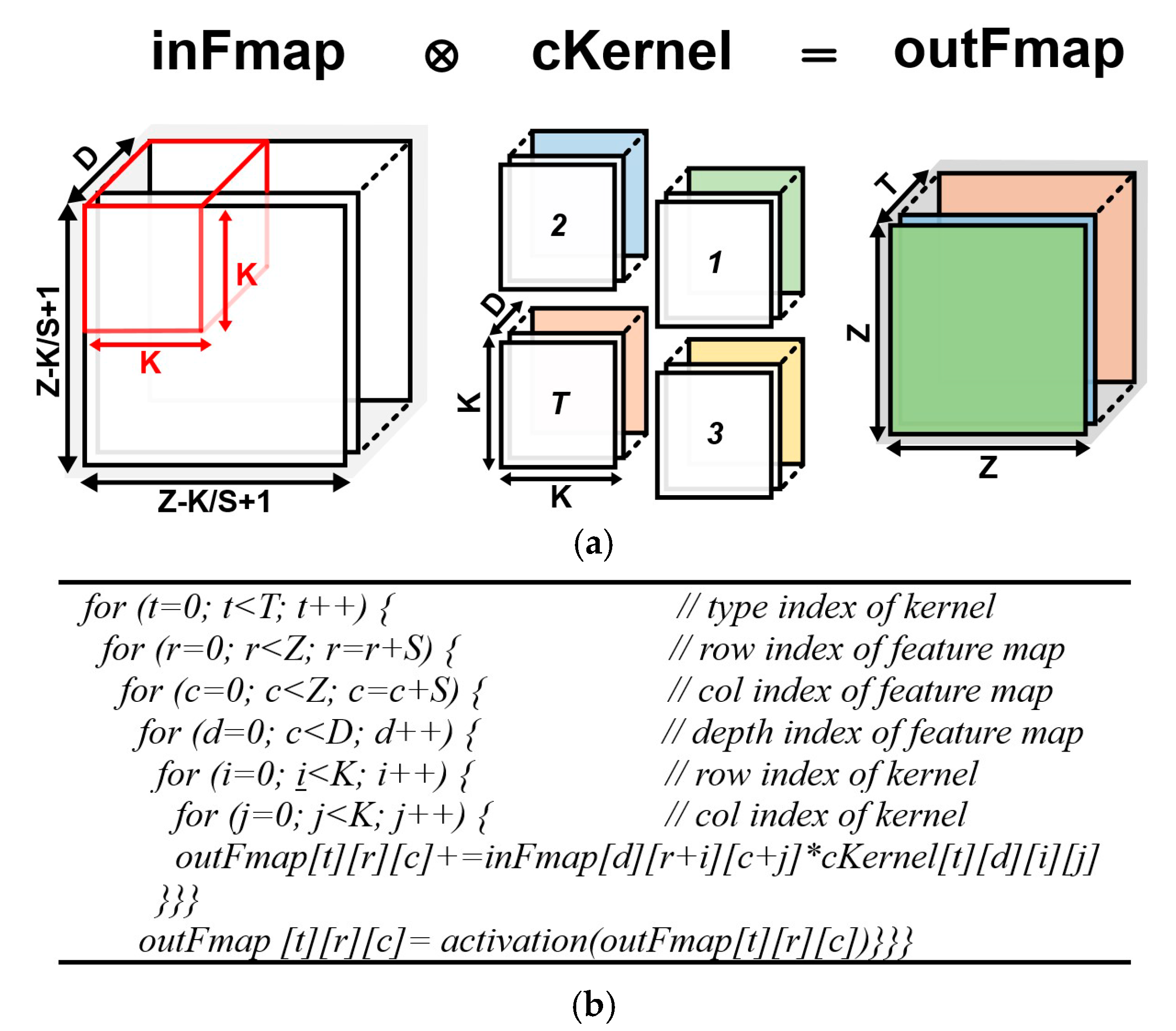
Figure 1. Convolution between convolution kernels and an input feature map. (a) Illustration of the convolution operation between one feature map and T type convolution kernels; (b) pseudo code of the convolution layer.
Electronics 09 00134 g001
Figure 2. Two types of hardware accelerators: (a) processing elements (PE) array structure and (b) reduction tree structure.
Electronics 09 00134 g002
Figure 3. Illustration of a 2 × 2 matrix multiplication step: (a) Strassen; (b) Naïve.
Electronics 09 00134 g003
Figure 4. Computational steps of a 2 × 2 matrix multiplication: (a) Strassen; (b) Naïve.
Electronics 09 00134 g004
Figure 5. Proposed 4 × 4 matrix multiplication method: (a) Partitioning of a 4 × 4 matrix into a 2 × 2 sub-matrices; (b) proposed matrix multiplication: Naïve (×) and Strassen (•).
Electronics 09 00134 g005
Figure 6. Cost-effective neural network accelerator (CENNA) architecture.
Electronics 09 00134 g006
Figure 7. Convolution operation inside CENNA architecture: (a) pseudo code of convolution layer inside CENNA; (b) equation of convolution using matrix multiplication; (c) Illustration of matrix multiplication.
Electronics 09 00134 g007
Figure 8. Generating partial sums row by row: (a) First; (b) Second; (c) Third; (d) Fourth.
Electronics 09 00134 g008
Figure 9. Tiling-based data reuse in CENNA: (a) example of overlapped elements in adjacent windows; (b) data tiling and memory hierarchy used for CENNA.
Electronics 09 00134 g009
Figure 10. Execution flow of the 6-stage pipeline in CENNA (6-stages: Load, 3-stage Matrix Multiplication, Convolution Operation and Store).
Electronics 09 00134 g010
Figure 11. Comparison of methods: (a) silicon area (mm2); (b) power consumption (mW).
Electronics 09 00134 g011
Table 1. Computation and parameter size requirements in a convolutional neural network [19].
CNN ModelAlexNet *VGG-16 **GoogLeNet ***ResNet-152 ****
Operation (MAC) 10.73 M16 G2 G11 G
Parameter Mem (Byte) 2233 M528 M51 M220 M
Number of operations (multiplication, addition) 1, Total weights including convolution kernel, bias 2, mm2) 2, Neural network designed by Alex khrizevsky */Visual geometry group **/Google ***, Residual network ****.
Table 2. Rough relative cost in 45 nm 0.9 V from Eyeriss [20].
OperationEnergy (pJ)Area (µm2)
MultiplierAdderMultiplierAdder
8-bit INT 10.2 pJ0.03 pJ282 µm236 µm2
16-bit FP 21.1 pJ0.4 pJ1640 µm21360 µm2
32-bit FP 23.7 pJ0.9 pJ7700 µm24184 µm2
Integer operation 1, Floating-point operation 2.
Table 3. Performance of the 4 × 4 pipelined matrix multiplication (16 bit MUL (M), 32 bit ADD (A)).
Cycle/Time (s) (109 4 × 4 Matrices)Maximum Frequency# of MUL/ADDAreaPower
Naïve 1(109 + 2)/2.00500 MHz64/480.270 mm221.45 mW
Strassen 2(109 + 3)/3.16370 MHz49/1980.203 mm221.70 mW
Cost-Centric 3(109 + 2)/2.00500 MHz56/1000.242 mm218.58 mW
3-stage (M-A-A) 1, 4-stage (A-2 × 2 Strassen-A-A) 2, 3-stage (A-2 × 2 Naïve-A) 3, Bold is a critical path.
Table 4. Summary of implementation evaluations of three neural network accelerators.
DesignNaïveStrassenCENNA
# of MUL/ADD64/10849/25856/160
Frequency500 MHz370 MHz500 MHz
Local Buffer 1448 B544 B400 B
SRAM64 KB64 KB64 KB
Area1.411 mm21.345 mm21.384 mm2
Power50.191 mW50.462 mW47.344 mW
Registers in accelerator (1st Addition, M1–M7, 2nd Addition, and Accumulator) 1.
Table 5. Inference performance of VGG-16 with 4 × 4 sized kernels and batch size 1.
LayerInput (W/H/C) 1Output (W/H/C)# of MAC (Giga)Total Time (ms) 2Memory Access Time (ms)
Conv1-1224 × 224 × 3224 × 224 × 640.164.860.29
Conv1-2224 × 224 × 64224 × 224 × 642.62103.616.09
Conv2-1112 × 112 × 64112 × 112 × 1281.2647.851.44
Conv2-2112 × 112 × 128112 × 112 × 1282.295.712.88
Conv3-156 × 56 × 12856 × 56 × 2561.4243.160.66
Conv3-256 × 56 × 25656 × 56 × 2562.8486.351.31
Conv3-356 × 56 × 25656 × 56 × 2562.8486.361.31
Conv4-128 × 28 × 25628 × 28 × 5121.2138.260.31
Conv4-228 × 28 × 51228 × 28 × 5122.4276.520.63
Conv4-328 × 28 × 51228 × 28 × 5122.4276.520.63
Conv5-114 × 14 × 51214 × 14 × 5120.4221.050.63
Conv5-214 × 14 × 51214 × 14 × 5120.4221.050.20
Conv5-314 × 14 × 51214 × 14 × 5120.4221.050.20
Total20.65722.3516.58
W/H/C: Width/Height/Channel 1, Including the computation time and memory access time 2.
Table 6. Comparison of inference performance running Conv1-1.
DesignNaïveStrassenCENNA
Total Time4.86 ms7.68 ms4.86 ms
Real Throughput 165.84 GOPS41.67 GOPS65.84 GOPS
Peak Throughput 286 GOPS63.64 GOPS86 GOPS
Efficiency 31.31 TOPS/W0.83 TOPS/W1.39 TOPS/W
Achievable performance (Giga-operation, GOPS) running convolution layer 1, Theoretical performance 2, Real throughput (Tera-operation) per watt 3.
Table 7. Performance comparison with PE-array based accelerators.
MetricsEyeriss [9]ConvNet [10]Chain-NN [11]CENNA
Precision (bit)161–161616
Process Technology (nm)65402865
Area (mm2) 112.252.410.691.38
Frequency (MHz)200204700500
# of operators 23362041152232
SRAM (KB)19214435264
Peak Throughput (GOPS)84102806.486
Real Throughput (GOPS) 324.663.38668.1657.17
Frame Rate (Frame/s) 30.61.5416.81.38
Power (mW) 4236220567.547.34
Scaled this metrics to 65 nm, 3.9 mm2/358 mW (ConvNet), 24.81 mm2/1,317 mW (Chain-NN) 1,4, Total number of multipliers and adders 2, VGG-16 scaled up to similar amount of computation as 20.65 giga MAC operations (GMAC) 3.
Table 8. Performance comparison with reduction tree-based implementations.
MetricsMAERI [12]Origami [13]CENNA
Precision (bit)161216
Process Technology (nm)286565
Area (mm2)3.843.091.38
Freq (MHz)200189500
# of operators336388232
SRAM (KB)804364
Peak Throughput (GOPS)67.27486
Real Throughput (GOPS) 158.275557.17
Frame Rate (Frame/s) 11.47.261.38
Power (mW)3709347.34
VGG-16 scaled up similar amount of computation as 20.65 GMAC 1.
Table 9. Efficiency comparison with the state-of-the-art works.
MetricEyeriss [9]ConvNet [10]Chain-NN [11]MAERI [12]Origami [13]CENNA
Power (TOPS/W)0.100.29 *1.18 *0.16 *0.591.21
Area (GOPS/mm2)2.0126.41 **62.5 **15.17 **17.8041.43
Overall (TOPS/W/mm2)0.010.12 ***0.11 ***0.04 ***0.190.88
If we scale the technology to 65 nm, ConvNet, Chain-NN, and MAERI are expected to 0.18/0.51/0.07 (TOPS/W) *, 16.25/28.22/7.67 (GOPS/mm2) **, and 0.05/0.02/0.01(TOPS/W/mm2) ***, respectively.