Article

A Fast Transient Response Digital LDO with a TDC-Based Signal Converter

College of Microelectronics, Faculty of Information Technology, Beijing University of Technology, Beijing 100124, China
*
Author to whom correspondence should be addressed.
Electronics 2020, 9(1), 132; https://doi.org/10.3390/electronics9010132
Submission received: 24 December 2019 / Revised: 7 January 2020 / Accepted: 8 January 2020 / Published: 10 January 2020
(This article belongs to the Special Issue Low-Voltage Integrated Circuits Design and Application)

Abstract

:
The digital low drop-out regulator (LDO) has been used widely in digital circuits for its low supply voltage characteristics. However, as the traditional digital LDOs regulate the output voltage code at a rate of 1 bit per clock cycle, the transient response speed is limited. This paper presents a digital LDO to improve transient response speed with a multi-bit conversion technique. The proposed technology uses a voltage sensor and a time-to-digital converter to convert the output voltage to digital codes. Based on a 65-nm CMOS process, the proposed DLDO reduces the settling time from 147.8 ns to 25.2 ns on average and the response speed is improved by about six times.

1. Introduction

Process scaling causes the continuous reduction in supply voltage. In particular, the application of the Internet of things (IoT) makes the low operating supply voltage more important than ever. In such conditions, dynamic range and bandwidth of integrated circuits are reduced, thus the stability is harder to control. The fine-grained supply voltage management faces a real challenge. In contrast to analog low drop-out regulator (LDO), digital LDOs (DLDO) exhibiting ultra-low operating voltage [1,2,3,4,5,6]. Hence, the DLDO has been widely used in the low source supply voltage conditions and digital load circuits.
The traditional DLDO employs a barrel shifter, whose output code switches 1 bit in a clock cycle [7]. When there is a large transient, it takes a long time to regulate the output voltage to the target value. Some studies have attempted to enhance the transient performance using adaptive regulation technology [8,9,10,11,12,13], but the circuit complexity increases obviously and the multiple times regulation is still required. In [14,15,16], DLDO with a flash analog-to-digital converter (ADC) is proposed. The ADC converts the output voltage to the digital domain and a digital controller provides a multi-bit regulation. Since the comparator offset increases the error of ADC, there may be a deviation in the regulation. In [17,18,19], a time-to-digital converter (TDC) is employed to replace ADC. To convert the output voltage to digital codes, the TDC alters the buffer-gate’s propagation delay by changing the power supply of the buffer-gate. However, the relationship between the power supply and the propagation delay of buffer-gate is nonlinear, and the resolution of TDC is degraded. In this paper, a voltage sensor based on capacitor charging is introduced. Since the proposed TDC operates by changing the time intervals rather than buffer-gate’s propagation delay, the linearity is improved. With a digital controller behind TDC, a multi-bit regulation is achieved and the transient response speed is increased.
This paper is organized as follows. Inl Section 2, the fast response DLDO is proposed with circuit architecture and system dynamic model. Section 3 discusses the circuit implementation of the proposed DLDO. In Section 4, the circuit performance is simulated and the simulation results are shown. Finally, conclusions are drawn in Section 5.

2. System Overview

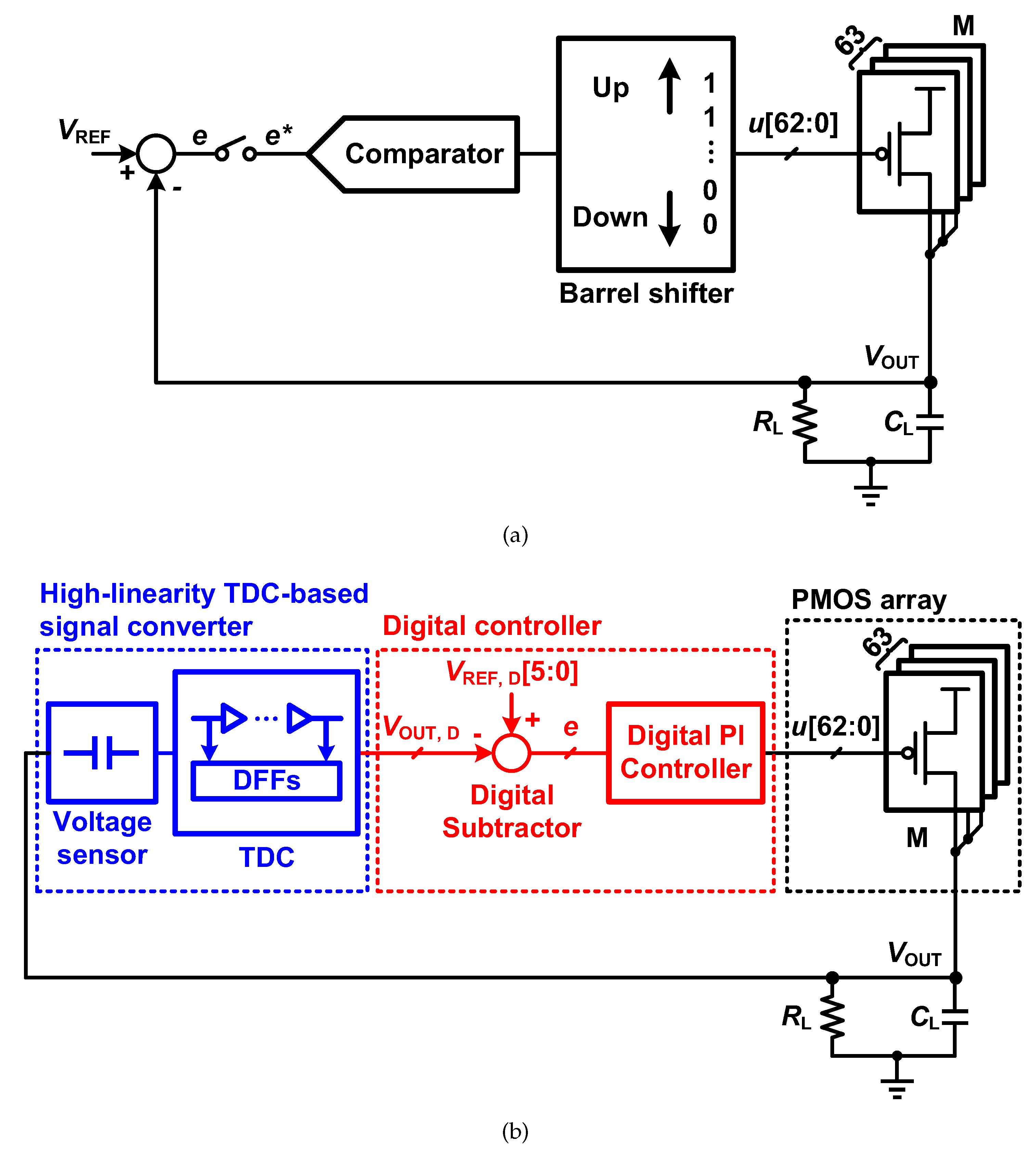
2.1. The Architecture of the Proposed DLDO

Figure 1 shows circuit diagrams for the baseline DLDO and the proposed DLDO. The proposed DLDO consists of three components. The first component is the TDC-based signal converter, which provides a digital code of the output voltage V OUT to a digital controller. As the second component, the digital controller outputs a regulation code to drive a PMOS array according to the different inputs. Finally, the PMOS array M provides appropriate current to regulate the V OUT .
In the TDC-based signal converter, a voltage sensor generates a time signal related to V OUT by capturing the charging time of a capacitor. The TDC behind the voltage sensor converts the time signal to a digital code V OUT , D . Subtracting V OUT , D from the reference voltage code V REF , D , the digital subtractor produces an error value e and drives the digital PI controller to vary the number of turned-on transistors in M. When the error value e is 0, V OUT , D is equal to V REF , D and output voltage V OUT is regulated to the target value.
In contrast to the conventional DLDO, the proposed circuit regulates its output voltage using a digital PI controller rather than a shift register. Hence, the number of turned-on transistors can be switched multi-bits in a clock cycle. A faster response is achieved in the proposed circuit.

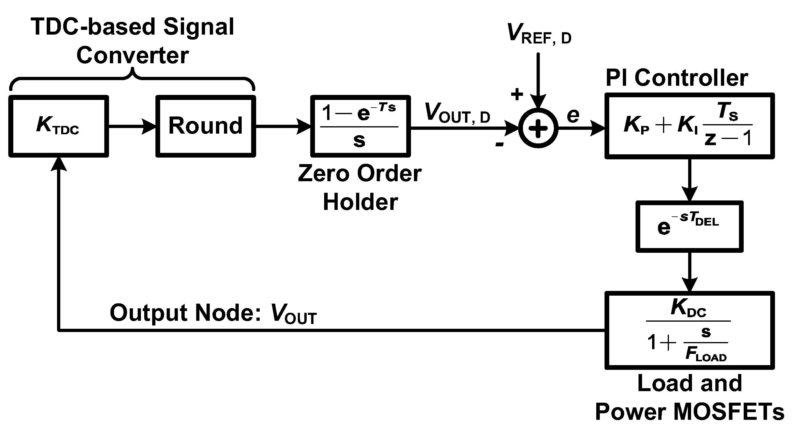
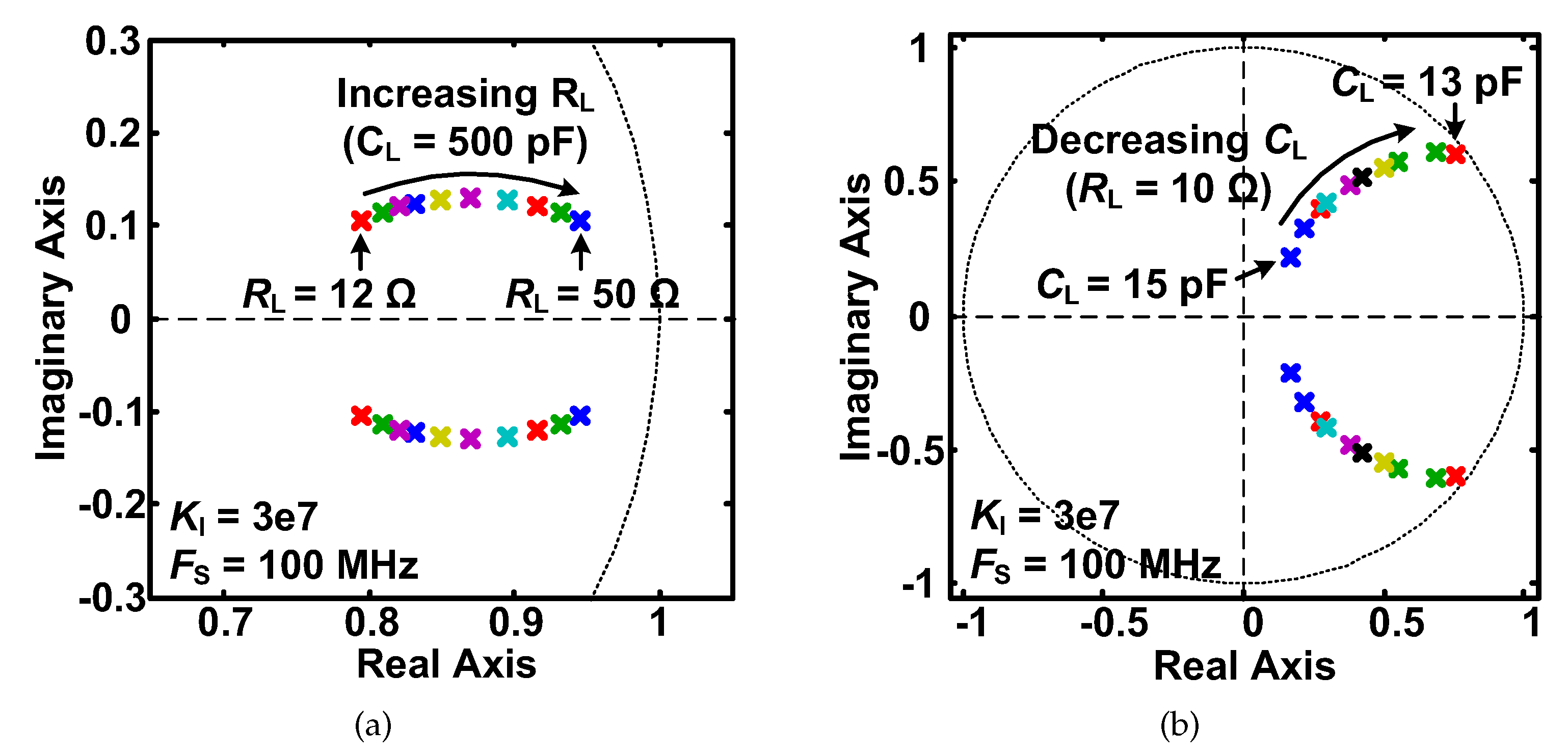
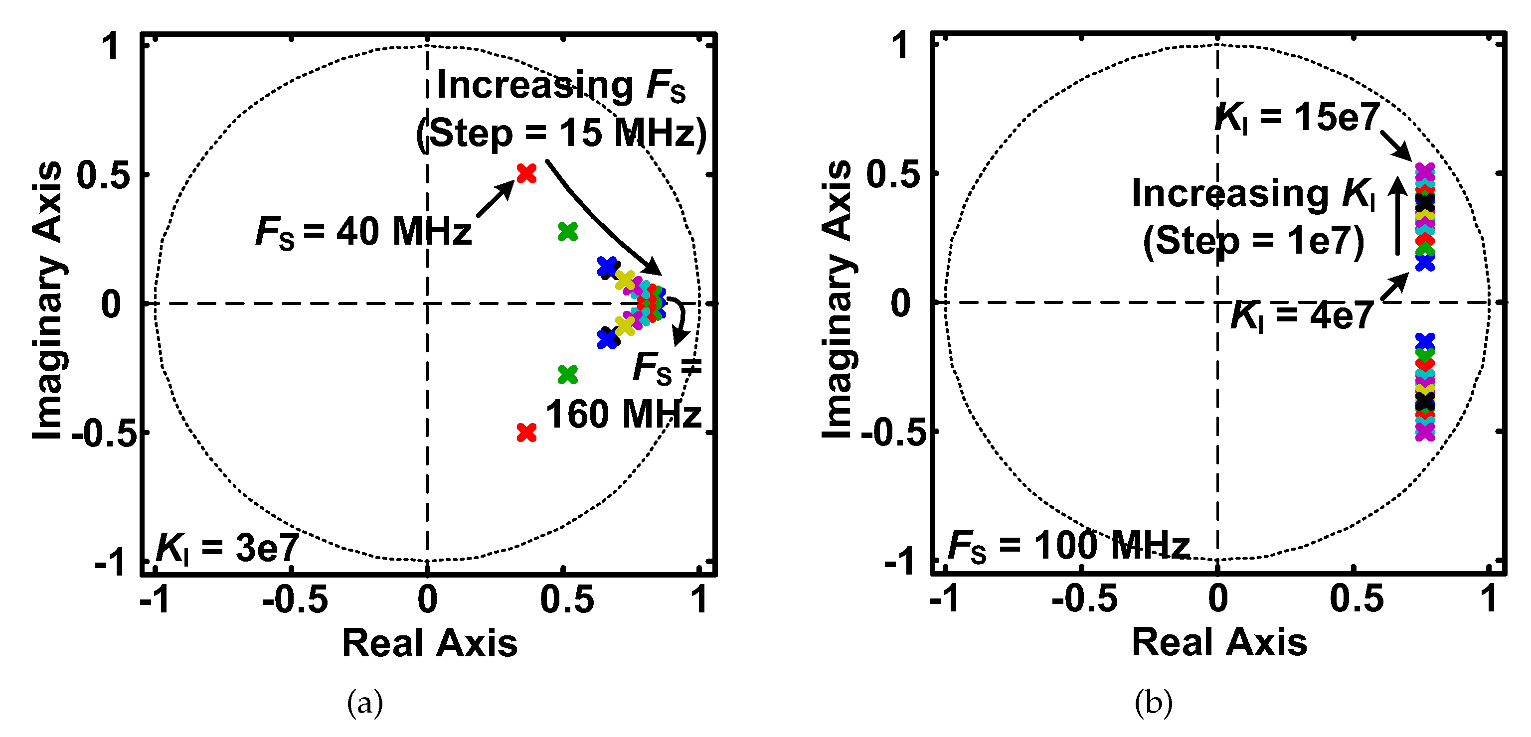
2.2. System Hybrid Model

To understand the overall system behavior, a system hybrid model for the proposed DLDO is shown in Figure 2. The relationship between input and output of the TDC-based signal converter is rounding linearly and the TDC-based signal converter is modeled as a cascade between gain K TDC and a rounding function. TDC-based signal converter operates periodically, and the rounding function is followed by a zero-order holder (ZOH). Since the digital PI controller accumulates the previous output of the digital subtractor, it acts as the superposition of a gain K p and an ideal integrator in discrete-time. The power MOSFETs are driven by a digital circuit, and their parasitic gate capacitances affect the settling time. The effect is modeled as a time delay e s T DEL , where T DEL is the delay caused by the parasitic gate capacitances. The corresponding transfer function in the z-domain is z T DEL . The load and power MOSFETs can be approximated as an R C load with gain K DC . The s-domain model of the load and power MOSFETs is
P s = K DC 1 + s F LOAD
where F LOAD is the output pole frequency and can be written as F LOAD = 1 / ( 2 π · R LOAD · C LOAD ) . The corresponding P ( z ) in z-domain can be represented as
P z = K DC F LOAD z z e F LOAD / F S
where F S is the sampling frequency and F S = 1 / T . Thus, the open-loop transfer function between V REF , D and V OUT can be written as
G z = K · z 1 T DEL z K p K I / F S K P z 1 z e F LOAD / F S
where the open-loop gain K = K DC K P F LOAD . Taking the TDC-based signal converter and the zero-order holder into account, the entire closed-loop transfer function of the proposed DLDO in z-domain is
Q z = K · z 1 T D E L z K P K I / F S K P z 2 + K TDC K z 2 T DEL 1 + e F LOAD / F S z K TDC K K P K I / F S K P z 1 T DEL + e F LOAD / F S
Because T DEL is much smaller than 1, Equation (4) can be approximated to
Q z = K · z z K P K I / F S K P 1 + K TDC K z 2 1 + e F LOAD / F S + K TDC K K P K I / F S K P z + e F LOAD / F S
Equation (5) provides insights into the stability of the proposed DLDO. Compared with the transfer function of the traditional DLDO in [20], the PI controller produces an extra zero at z = K P K I / F S / K P . The bandwidth and transient response speed of the proposed system are increased.
Figure 3 shows the pole plots of the proposed system under different sampling frequency and integration gain conditions. The simulation parameters are listed in Table 1. As illustrated in the plots, a large sampling frequency damages the system stability. In addition, the higher integration gain of the digital PI controller leads to decreasing stability. Hence, large F S and K I should be avoided in the selection of parameters. In Figure 4, the pole plots of the proposed system under variable load are shown and the simulation parameters in Table 1 are used. As illustrated in the plots, the increasing load resistance, which results in a lower load current, reduces the stability of the proposed system. Meanwhile, the decreasing load capacitance degrades the system stability as well. When the load capacitance is decreased to 13 pF, the pole is close to the unit circle, and the system is in critical stability.

3. Circuit Implementation
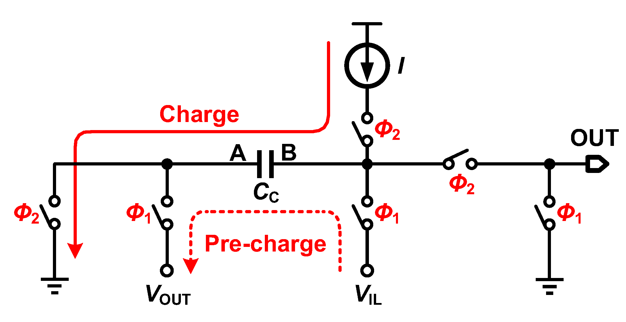
3.1. Voltage Sensor

The transformation of the output voltage from analog to digital is achieved by a TDC-based signal converter, which contains a voltage sensor and a time-to-digital converter. Figure 5 illustrates the circuit scheme of the voltage sensor. During phase ϕ 1 , two plates of the charge capacitor C C are pre-charge to V OUT and V IL , respectively, where V IL is the acceptable high level of the buffer-gate in TDC. After the capacitor is pre-charged, the voltage difference between node A and node B is ( V OUT V IL ). At the moment the phase is switched, node A is connected to ground. Because the voltage difference between the two plates of a capacitor does not change suddenly, the voltage of node B is ( V IL V OUT ). During phase ϕ 2 , node B is charged by a constant current source I, which is supplied by a PMOS of a current mirror. Since V IL is usually lower than half the supply voltage, the source-drain voltage of the PMOS is large enough and the PMOS operates in the saturation region. Under such a condition, the drain current is slightly affected by the source-drain voltage. Hence, the linearity of the voltage sensor is not greatly affected by the change of the voltage of node B. The charging current I is stable in the range of concern.
When the voltage of node B rises to V IL , the voltage level turns to logic “1” and the TDC is triggered. During the process, the charge variation in C C can be expressed as
Δ Q C = I · Δ t
where Δ t is the time interval of node B is charged from ( V IL V OUT ) to V IL . Meanwhile, the voltage variation of node B is [ V IL −( V IL V OUT )]. The relationship between Δ Q C and the voltage change during Δ t is
Δ Q C = C C · V IL V IL V OUT
Combining Equations (6) and (7), Δ t can be expressed as
Δ t = C C I V OUT
Hence, the output voltage is converted to a time interval by varying the initial voltage of C C .
In the voltage sensor, a parasitic capacitance exists in the capacitor C C , which causes a slight change of about 20–30 fF in C C . In the proposed circuit, the charging capacitance is 250 fF, which is much larger than the parasitic capacitance. Because the resolution of the proposed 6-bit TDC-based voltage converter is about 25 mV, the circuit response is not modified by the slight fluctuation of C C .

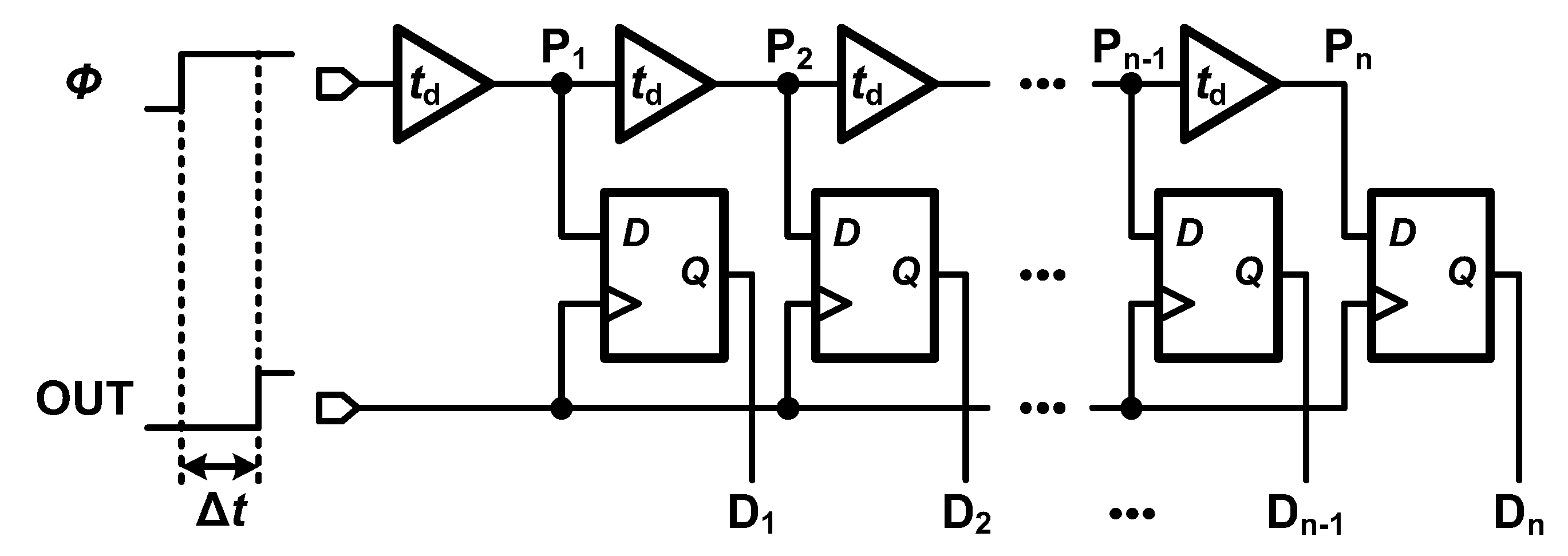
3.2. Time-to-Digital Converter

The circuit scheme of the time-to-digital converter is shown in Figure 6. As an all digital circuits, TDC is implemented by logical synthesis. The input ports of the TDC are connected to the clock ϕ and the output of the voltage sensor. In the delay line, the propagated time of each buffer is t d . Figure 7 shows the timing diagram of the TDC-based signal converter. At the beginning of phase ϕ 2 , signal “1” is transmitted in the delay line. When the voltage sensor generates a positive edge, the D flip-flops are triggered, and ports D i (i = 1, 2, ⋯, n) output the voltage level of node P i (i = 1, 2, ⋯, n). The number of buffers transmitted by signal “1” is N = Δ t / t d . According to Equation (8),
N = C C I · t d V OUT
Using the voltage sensor and TDC, the transformation of V OUT from analog to digital can be achieved.

3.3. Digital Controller

The delay line in TDC outputs a 64-bit thermometer-coded digital signal V OUT , D . The digital subtractor subtracts the temperature code from the reference voltage V REF , D and outputs an error value e. Driven by the error value, the output of the digital PI controller at kth clock cycle can be expressed as
u k = K P e k + K I j = 0 k e j
When there is a steady-state error, V OUT , D is not equal to the V REF , D and the output of digital subtractor is non-zero. Under such a condition, the accumulative component of Equation (10) causes the PI to output a variable value. The digital code V OUT , D is forced to approach the V REF , D until steady-state error is eliminated. When the circuit is stable, V OUT , D is equal to the V REF , D and the output of the digital subtractor is 0. Since the accumulative component of the digital PI controller no longer changes, a stable voltage is outputted continuously.

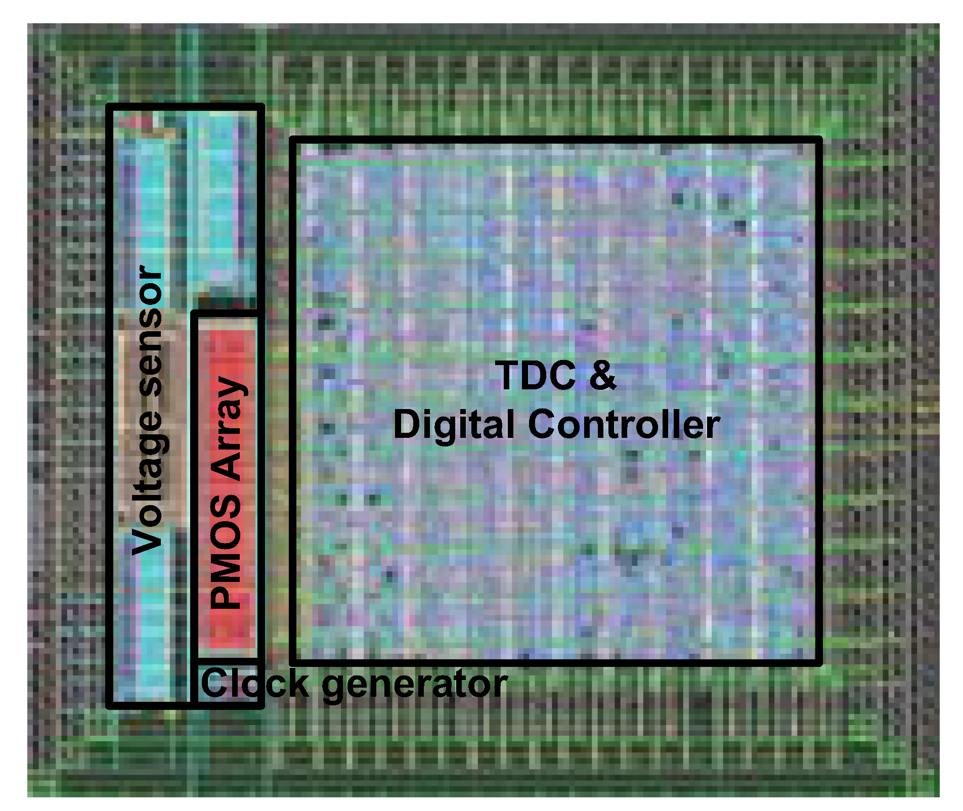
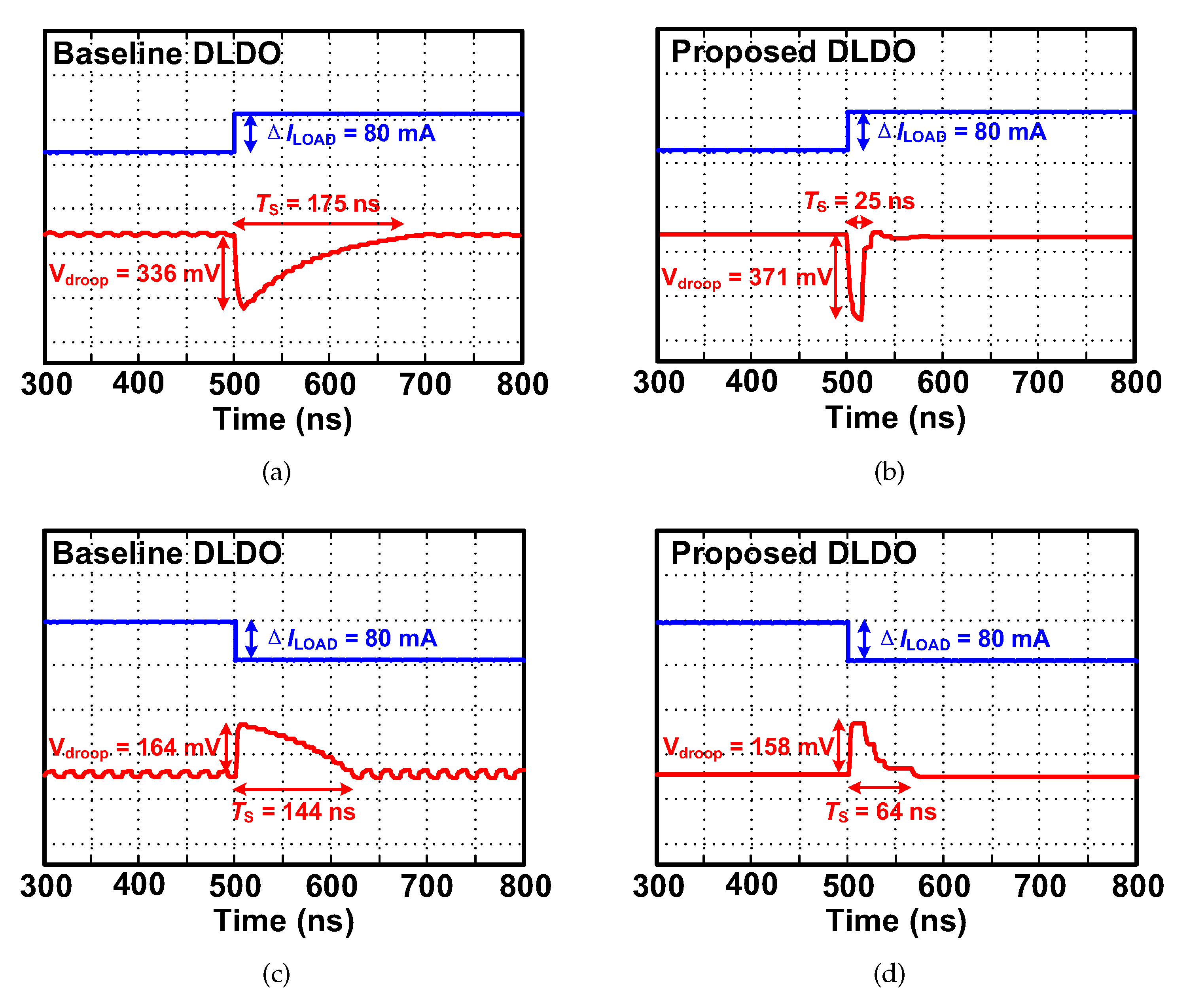
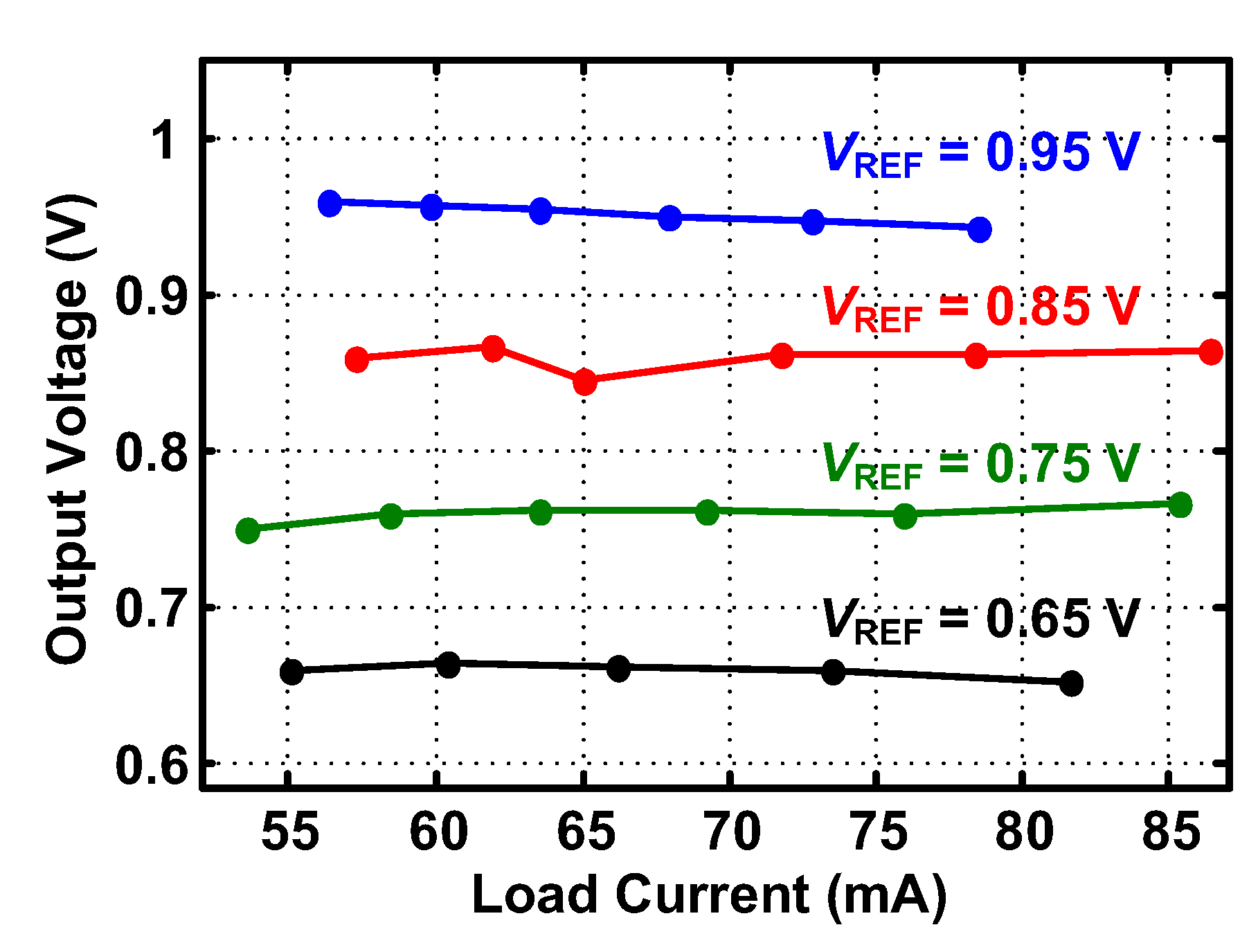
4. Simulation and Results

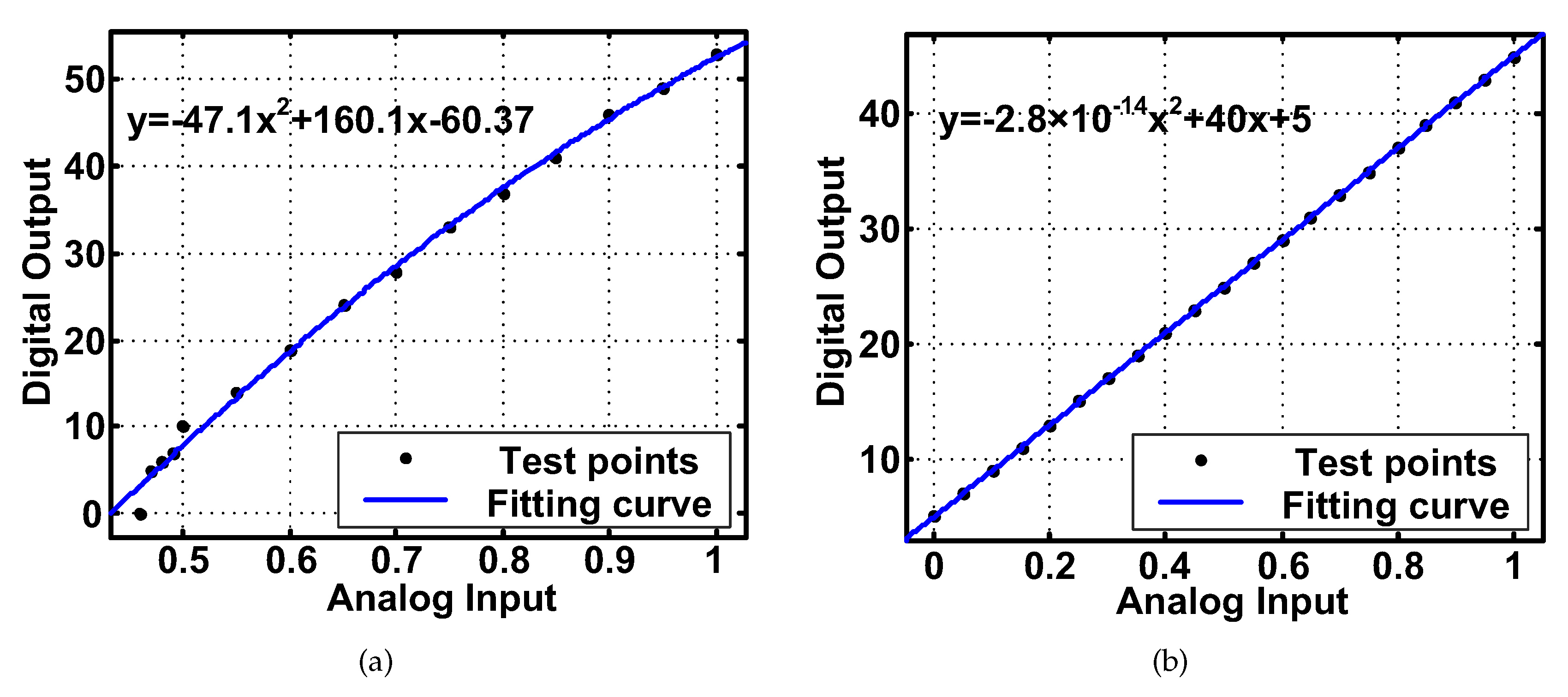
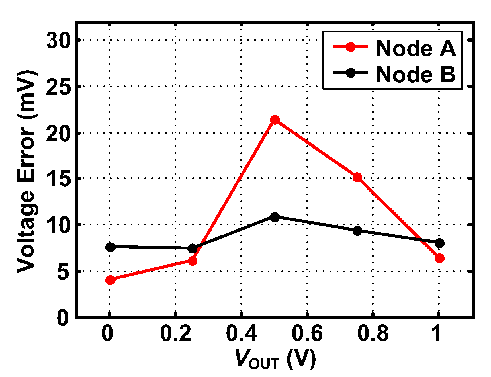
4.1. TDC-Based Signal Converter
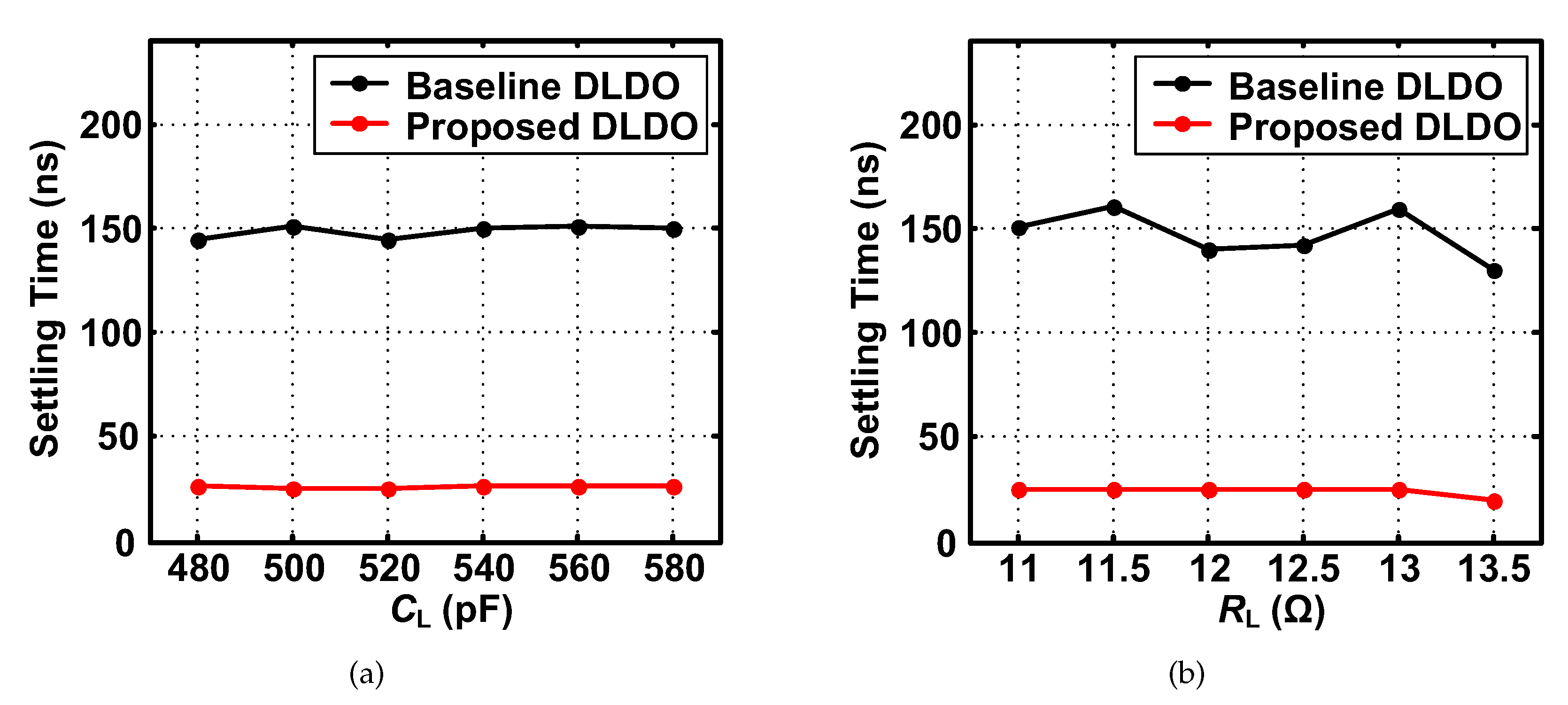
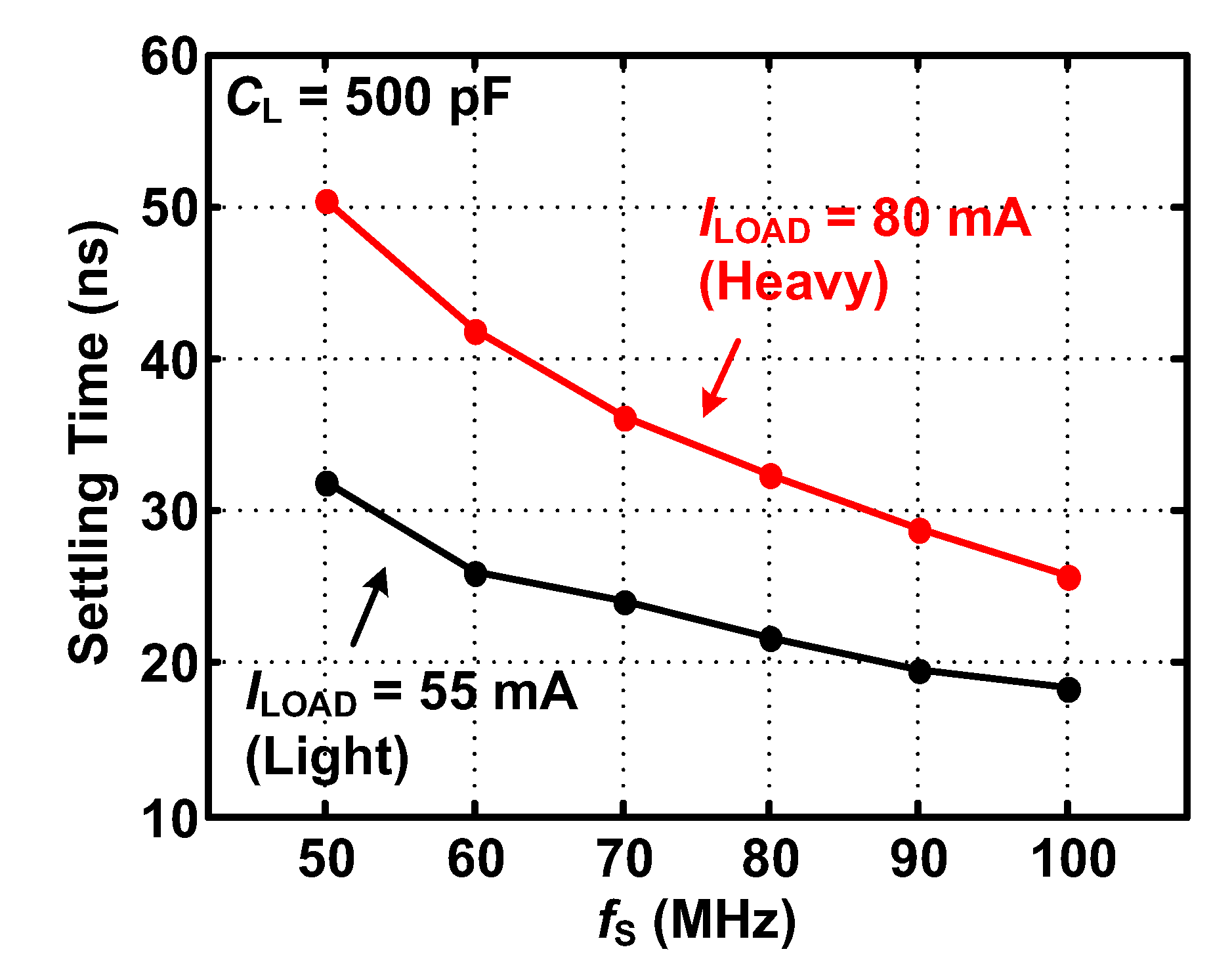
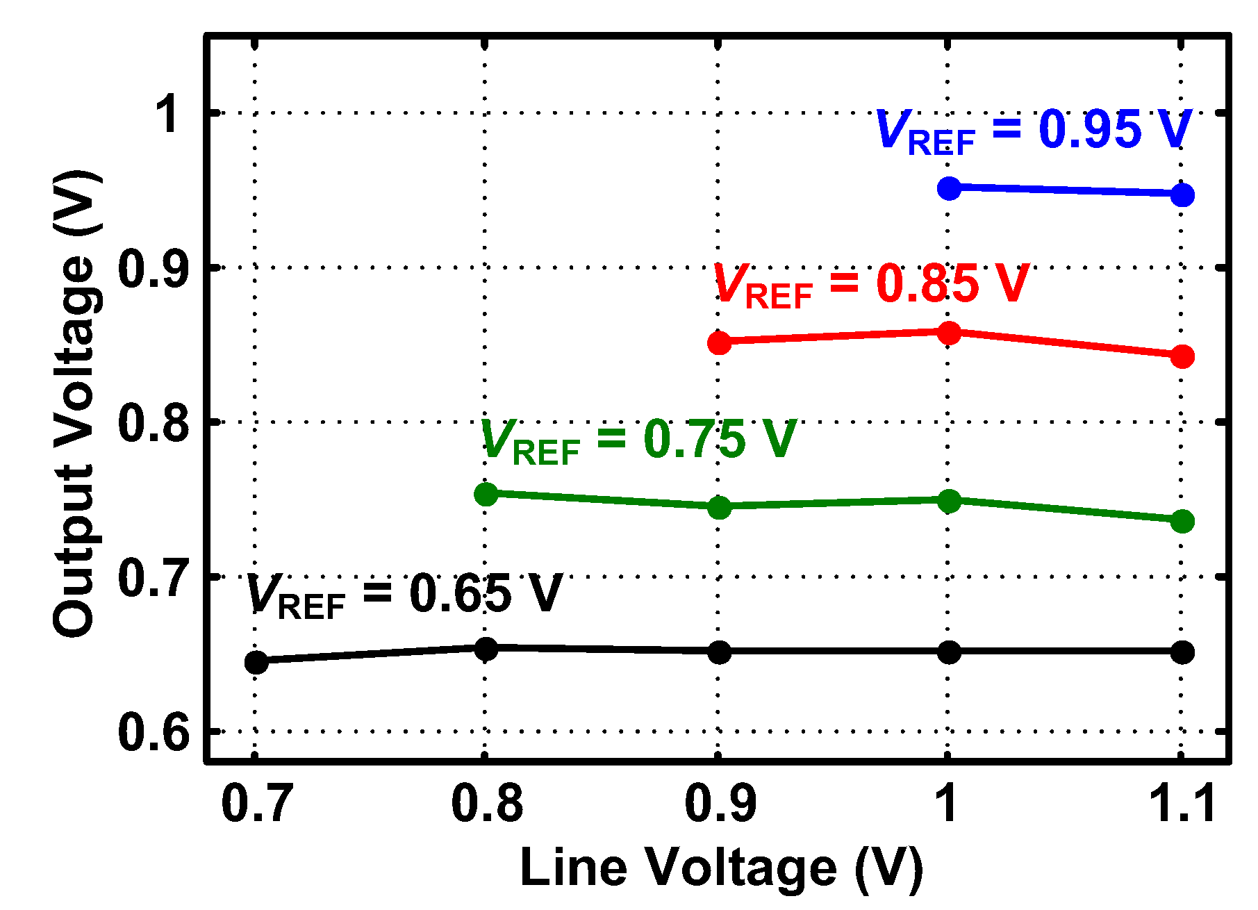
The proposed fast response DLDO was realized in a 65-nm TSMC technology. It occupies an active area of 0.017 mm 2 and the layout is shown in Figure 8. The current injection of the switches in the TDC-based voltage converter introduces the voltage errors to the output voltage of switches. To describe the effect, the voltage errors were measured and the results are shown in Figure 9. In the circuit, the charging capacitor is 250 fF and the charging current I is 120 μ A. According to the results, the current injection causes the positive errors at node A and node B under different V OUT conditions. The resolution of the proposed TDC-based voltage converter is about 25 mV, which is larger than the maximum voltage error. Hence, the current injection will not affect the accuracy of the proposed circuit. Figure 10 shows the comparison of linearity between the conventional TDC and the proposed TDC. The test points are fitted into a quadratic function. According to the fitting results, the coefficients of the quadratic term of the conventional TDC and the proposed TDC are −47.1 and 2 . 8 × 10 14 , respectively. Relative to the conventional TDC, the performance of linearity is improved in the proposed design.

4.2. Proposed DLDO

To describe the transient response speed of the proposed circuit, the settling time T S with variable load was simulated. The settling time is defined as the time of the output voltage recovers to 90% of the droop voltage. As shown in Figure 11, the proposed DLDO reduces the settling time under each condition. The settling time is decreased to only 17.1% of the baseline design of DLDO (from 147.8 ns to 25.2 ns) on average. In other words, the proposed circuit improves the response speed by about six times. Under the variations of sampling frequency and load current, the settling time was evaluated as well. In Figure 12, the increasing sampling frequency results in a shorter T S . The settling time when f S = 100 MHz is about half that of f S = 50 MHz. Compared with the heavy load condition, settling time is shorter in the light load condition under each frequency.
Figure 13 shows the measured transient responses of the baseline DLDO and the proposed DLDO with a load step of 80 mA. With V IN = 1 V, V OUT = 0.85 V (step up) or V OUT = 0.65 V (step down), f S = 100 MHz and C L = 500 pF, we measured a 25 ns (step up) or 64 ns (step down) settling time. Compared with the baseline case, the proposed DLDO shows a significantly faster settling time. The output voltage is measured for a target voltage of from 0.95 to 0.65 V with V IN ranging from 0.7 to 1.1 V. As shown in Figure 14, the effect of the line voltage on the output voltage is slight. A line regulation of 15 mV/V is achieved. The output voltage with a load current range from 55 to 85 mA is measured. As shown in Figure 15, the circuit regulates the output voltage from 0.95 to 0.65 V, and a load regulation of <0.8 mV/mA is achieved. A performance comparison with published DLDO is given in Table 2, which includes both the ALDO and DLDO. In comparison to those prior designs in Table 2, this paper achieves the shortest response time, the best figure of merit (FOM) of speed [21], and competitive current efficiency.

5. Conclusions

This paper presents a fast response DLDO with a TDC-based signal converter for decreasing the settling time. The voltage sensor and TDC convert the output voltage from analog to digital. The digital controller provides a multi-bit regulation and improves transient response performance. The simulation results show that the proposed fast response DLDO can decrease the settling time to 17.1% of the baseline design of DLDO on average, and a FOM of 8.7 ps is achieved.

Author Contributions

Conceptualization, H.Z., J.G., and Z.C.; Data curation, P.W. and Z.L; Investigation, J.G. and Z.L.; Methodology, H.Z. and J.G.; Resources, P.W. and Z.C.; Writing—original draft, H.Z.; and Writing—review and editing, P.W. and Z.C. All authors have read and agreed to the published version of the manuscript.

Funding

This work was supported by Beijing Natural Science Foundation Project No.4184083, and National Natural Science Foundation of China, Key Project No.61731019.

Conflicts of Interest

The authors declare no conflict of interest.

References

  1. Ma, X.; Lu, Y.; Martins, R.P.; Li, Q. A 0.4 V 430nA quiescent current NMOS digital LDO with NAND-based analog-assisted loop in 28 nm CMOS. In Proceedings of the 2018 IEEE International Solid-State Circuits Conference-(ISSCC), San Francisco, CA, USA, 11–15 February 2018; pp. 306–308. [Google Scholar]
  2. Oh, T.J.; Hwang, I.C. A 110-nm CMOS 0.7-V input transient-enhanced digital low-dropout regulator with 99.98% current efficiency at 80-mA load. IEEE Trans. Very Large Scale Integr. (VLSI) Syst. 2014, 23, 1281–1286. [Google Scholar] [CrossRef]
  3. Li, Y.; Zhang, X.; Zhang, Z.; Lian, Y. A 0.45-to-1.2-V fully digital low-dropout voltage regulator with fast-transient controller for near/subthreshold circuits. IEEE Trans. Power Electron. 2015, 31, 6341–6350. [Google Scholar] [CrossRef]
  4. Yang, F.; Mok, P.K. A nanosecond-transient fine-grained digital LDO with multi-step switching scheme and asynchronous adaptive pipeline control. IEEE J. Solid-State Circuits 2017, 52, 2463–2474. [Google Scholar] [CrossRef]
  5. Huang, M.; Lu, Y.; Seng-Pan, U.; Martins, R.P. An output-capacitor-free analog-assisted digital low-dropout regulator with tri-loop control. In Proceedings of the 2017 IEEE International Solid-State Circuits Conference-(ISSCC), San Francisco, CA, USA, 5–9 February 2017; pp. 342–343. [Google Scholar]
  6. Salem, L.G.; Warchall, J.; Mercier, P.P. A 100 nA-to-2 mA successive-approximation digital LDO with PD compensation and sub-LSB duty control achieving a 15.1 ns response time at 0.5 V. In Proceedings of the 2017 IEEE International Solid-State Circuits Conference-(ISSCC), San Francisco, CA, USA, 5–9 February 2017; pp. 340–341. [Google Scholar]
  7. Okuma, Y.; Ishida, K.; Ryu, Y.; Zhang, X.; Chen, P.H.; Watanabe, K.; Sakurai, T. 0.5-V input digital LDO with 98.7% current efficiency and 2.7-μA quiescent current in 65nm CMOS. In Proceedings of the IEEE Custom Integrated Circuits Conference, San Jose, CA, USA, 19–22 September 2010; pp. 1–4. [Google Scholar]
  8. Lee, J.; Bang, J.; Lim, Y.; Choi, J. A 0.5 VV IN, 0.29 ps-Transient-FOM, and Sub-2mV-Accuracy Adaptive-Sampling Digital LDO Using Single-VCO-Based Edge-Racing Time Quantizer. In Proceedings of the 2019 Symposium on VLSI Circuits, Kyoto, Japan, 9–14 June 2019; pp. C130–C131. [Google Scholar]
  9. Nasir, S.B.; Gangopadhyay, S.; Raychowdhury, A. A 0.13 μm fully digital low-dropout regulator with adaptive control and reduced dynamic stability for ultra-wide dynamic range. In Proceedings of the 2015 IEEE International Solid-State Circuits Conference-(ISSCC), San Francisco, CA, USA, 22–26 February 2015; pp. 1–3. [Google Scholar]
  10. Kundu, S.; Liu, M.; Wong, R.; Wen, S.J.; Kim, C.H. A fully integrated 40 pF output capacitor beat-frequency-quantizer-based digital LDO with built-in adaptive sampling and active voltage positioning. In Proceedings of the 2018 IEEE International Solid-State Circuits Conference-(ISSCC), San Francisco, CA, USA, 11–15 February 2018; pp. 308–310. [Google Scholar]
  11. Nasir, S.B.; Sen, S.; Raychowdhury, A. Switched-mode-control based hybrid LDO for fine-grain power management of digital load circuits. IEEE J. Solid-State Circuits 2017, 53, 569–581. [Google Scholar] [CrossRef]
  12. Tsou, W.J.; Yang, W.H.; Lin, J.H.; Chen, H.; Chen, K.H.; Wey, C.L.; Tsai, T.Y. Digital low-dropout regulator with anti PVT-variation technique for dynamic voltage scaling and adaptive voltage scaling multicore processor. In Proceedings of the 2017 IEEE International Solid-State Circuits Conference-(ISSCC), San Francisco, CA, USA, 5–9 February 2017; pp. 338–339. [Google Scholar]
  13. Kundu, S.; Liu, M.; Wen, S.J.; Wong, R.; Kim, C.H. A Fully Integrated Digital LDO With Built-In Adaptive Sampling and Active Voltage Positioning Using a Beat-Frequency Quantizer. IEEE J. Solid-State Circuits 2018, 54, 109–120. [Google Scholar] [CrossRef]
  14. Kim, D.; Seok, M. A fully integrated digital low-dropout regulator based on event-driven explicit time-coding architecture. IEEE J. Solid-State Circuits 2017, 52, 3071–3080. [Google Scholar] [CrossRef]
  15. Kim, D.; Kim, J.; Ham, H.; Seok, M. A 0.5 VV IN 1.44 mA-class event-driven digital LDO with a fully integrated 100 pF output capacitor. In Proceedings of the 2017 IEEE International Solid-State Circuits Conference-(ISSCC), San Francisco, CA, USA, 5–9 February 2017; pp. 346–347. [Google Scholar]
  16. Ding, Z.; Xu, X.; Song, H.; Rhee, W.; Wang, Z. Flash ADC-based digital LDO with non-linear decoder and exponential-ratio array. Electron. Lett. 2019, 55, 585–587. [Google Scholar] [CrossRef]
  17. Lim, C.; Mandal, D.; Bakkaloglu, B.; Kiaei, S. A 50-mA 99.2% peak current efficiency, 250-ns settling time digital low-dropout regulator with transient enhanced PI controller. IEEE Trans. Very Large Scale Integr. (VLSI) Syst. 2017, 25, 2360–2370. [Google Scholar] [CrossRef]
  18. Otsuga, K.; Onouchi, M.; Igarashi, Y.; Ikeya, T.; Morita, S.; Ishibashi, K.; Yanagisawa, K. An on-chip 250 mA 40 nm CMOS digital LDO using dynamic sampling clock frequency scaling with offset-free TDC-based voltage sensor. In Proceedings of the 2012 IEEE International SOC Conference, Falls, NY, USA, 12–14 September 2012; pp. 11–14. [Google Scholar]
  19. Ojima, N.; Nakura, T.; Iizuka, T.; Asada, K. A synthesizable digital low-dropout regulator based on voltage-to-time conversion. In Proceedings of the 2018 IFIP/IEEE International Conference on Very Large Scale Integration (VLSI-SoC), Verona, Italy, 8–10 October 2018; pp. 55–58. [Google Scholar]
  20. Nasir, S.B.; Gangopadhyay, S.; Raychowdhury, A. All-digital low-dropout regulator with adaptive control and reduced dynamic stability for digital load circuits. IEEE Trans. Power Electron. 2016, 31, 8293–8302. [Google Scholar] [CrossRef]
  21. Hazucha, P.; Karnik, T.; Bloechel, B.A.; Parsons, C.; Finan, D.; Borkar, S. Area-efficient linear regulator with ultra-fast load regulation. IEEE J. Solid-State Circuits 2005, 40, 933–940. [Google Scholar] [CrossRef]
  22. Chen, L.; Cheng, Q.; Guo, J.; Chen, M. High-PSR CMOS LDO with embedded ripple feedforward and energy-efficient bandwidth extension. In Proceedings of the 2015 28th IEEE International System-on-Chip Conference (SOCC), Beijing, China, 8–11 September 2015; pp. 384–389. [Google Scholar]
  23. Ding, Z.; Rhee, W.; Wang, Z. A VCO-dedicated digital LDO with multi-comparator coarse loop and 1-bit ΔΣ fine loop for robust frequency generation. In Proceedings of the 2018 IEEE MTT-S International Wireless Symposium (IWS), Chengdu, China, 6–10 May 2018; pp. 1–4. [Google Scholar]
  24. Adorni, N.; Stanzione, S.; Boni, A. A 10-mA LDO With 16-nA IQ and Operating From 800-mV Supply. IEEE J. Solid-State Circuits 2019, 1–10. [Google Scholar] [CrossRef]
  25. Kim, S.J.; Kim, D.; Ham, H.; Kim, J.; Seok, M. A 67.1-ps FOM, 0.5-V-hybrid digital LDO with asynchronous feedforward control via slope detection and synchronous PI with state-based hysteresis clock switching. IEEE Solid-State Circuits Lett. 2018, 1, 130–133. [Google Scholar] [CrossRef]
Figure 1. The circuit architecture of (a) baseline DLDO and (b) proposed DLDO.
Electronics 09 00132 g001
Figure 2. The system hybrid model for the proposed DLDO.
Electronics 09 00132 g002
Figure 3. The pole plot of the proposed system under: (a) variable sampling frequency; and (b) variable integration gain.
Electronics 09 00132 g003
Figure 4. The pole plot of the proposed system under: (a) variable load resistance; and (b) variable load capacitance.
Electronics 09 00132 g004
Figure 5. The circuit scheme of the voltage sensor.
Electronics 09 00132 g005
Figure 6. The circuit scheme of the time-to-digital converter.
Electronics 09 00132 g006
Figure 7. The timing diagram of the TDC-based signal converter.
Electronics 09 00132 g007
Figure 8. The layout of the proposed fast response DLDO.
Electronics 09 00132 g008
Figure 9. The voltage error caused by the current inject of switches.
Electronics 09 00132 g009
Figure 10. The comparison of linearity for: (a) conventional TDC; and (b) proposed TDC.
Electronics 09 00132 g010
Figure 11. The settling time when: (a) load resistance is 11 Ω ; and (b) load capacitance is 500 pF.
Electronics 09 00132 g011
Figure 12. The settling time under the variations of sampling frequency and load current.
Electronics 09 00132 g012
Figure 13. The measured transient responses of the baseline DLDO and the proposed DLDO for a load: step up (a,b); and step down (c,d).
Electronics 09 00132 g013
Figure 14. The output voltage under the variations of line voltage.
Electronics 09 00132 g014
Figure 15. The output voltage under the variations of load current.
Electronics 09 00132 g015
Table 1. The simulation parameters of the system hybrid model.
K P K TDC K DC R LOAD C LOAD F LOAD T DEL
1380.0210 Ω 500 pF32 MHz10 ps
Table 2. Comparison with published LDO designs.
Paper2015 [22]2018 [23]2019 [24]2018 [25]This Work
TypeAnalogDigitalAnalogDigitalDigital
Process180 nm65 nm55 nm65 nm65 nm
Active area [mm 2 ]0.021NA0.0420.0120.017
V IN [V]1.3–1.80.8–1<0.80.5–10.7–1.1
V OUT [V]1.20.75–0.950.60.35–0.950.65–1.05
Quiescent I Q [ μ A]10240.01645.2495
I MAX [mA]2513102.8120
Peak current efficiency η [%]99.999.899.898.499.6
Line regulation [mV/V]0.5NA0.5NA15
Load regulation [mV/mA]0.14NA1.05NA0.6
Load capacitor C L [nF]47000.210000.10.5
Max voltage droop [mV] @
Load step
2 @
25 mA
100 @
6 mA
70 @
10 mA
46 @
1.76 mA
371 @
80 mA
Response time T R * [ns]3763.370002.632.1
FOM ** [ps]15013.311.467.18.7
* T R = C L V droop / I MAX ; ** FOM = T R I Q / I MAX .

