Solving Overlapping Pattern Issues in On-Chip Learning of Bio-Inspired Neuromorphic System with Synaptic Transistors


Abstract
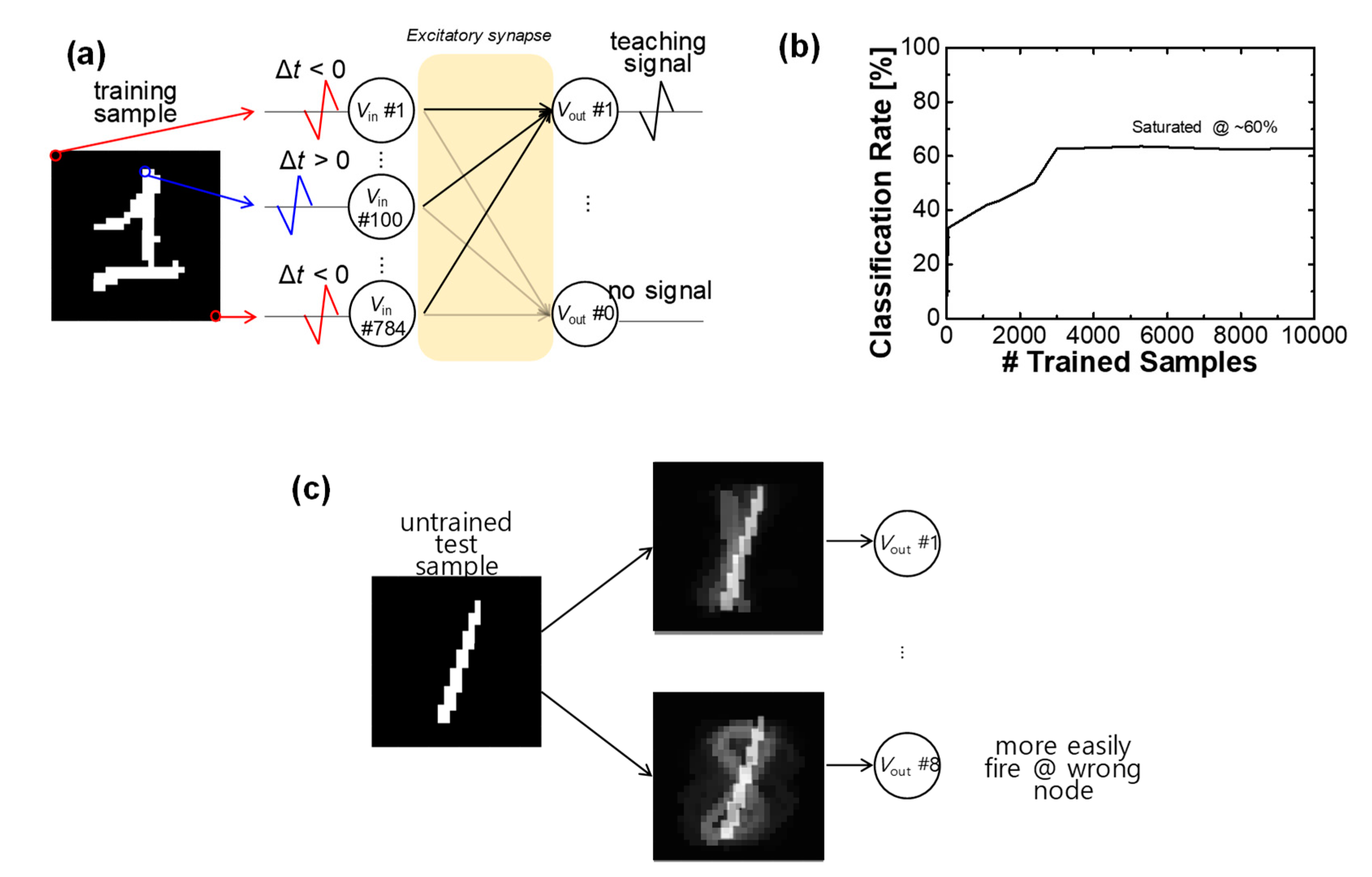
:1. Introduction
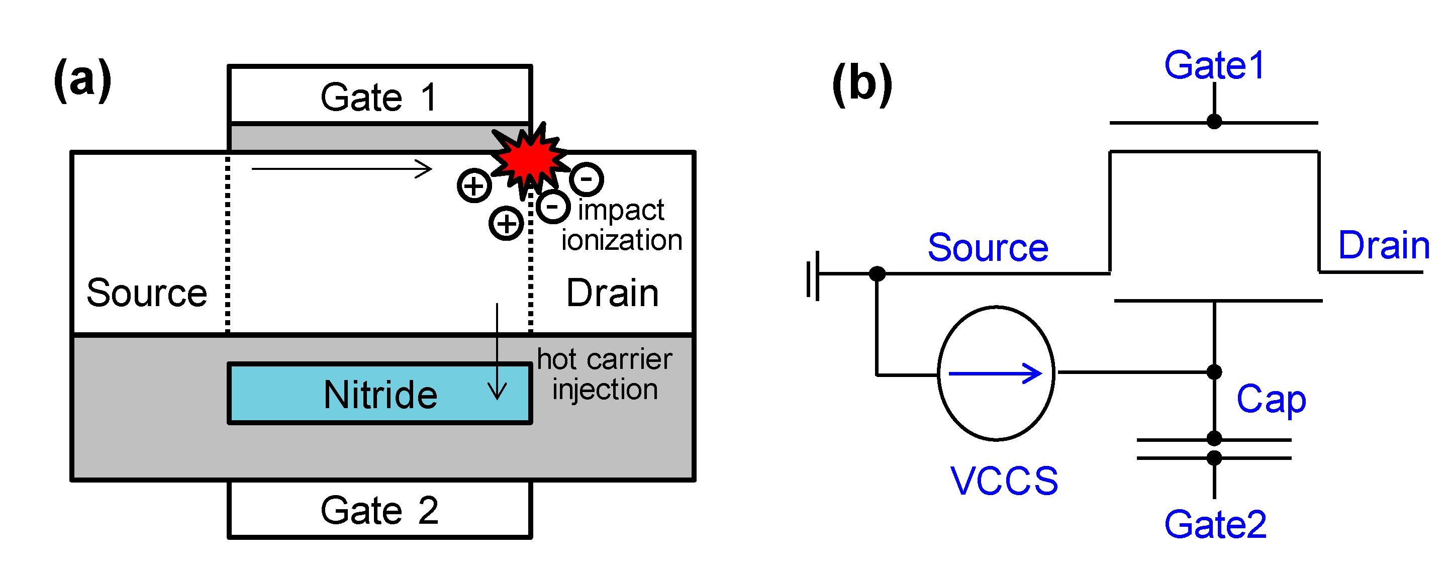
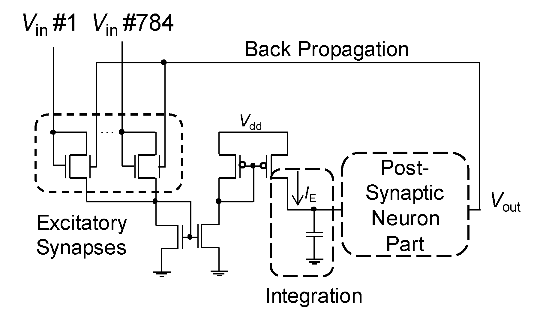
2. Device Model of Synaptic Transistor for System-Level Study
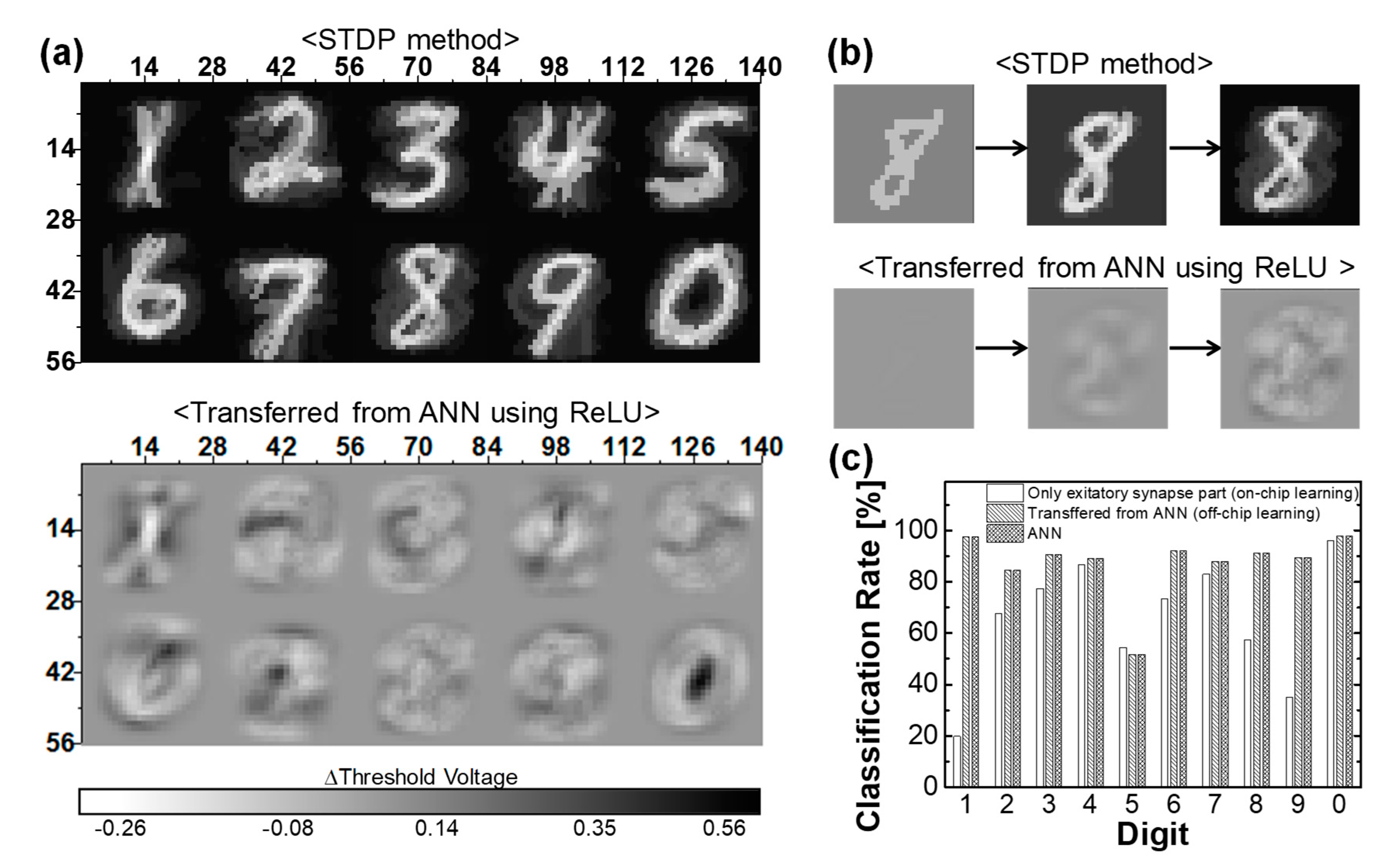
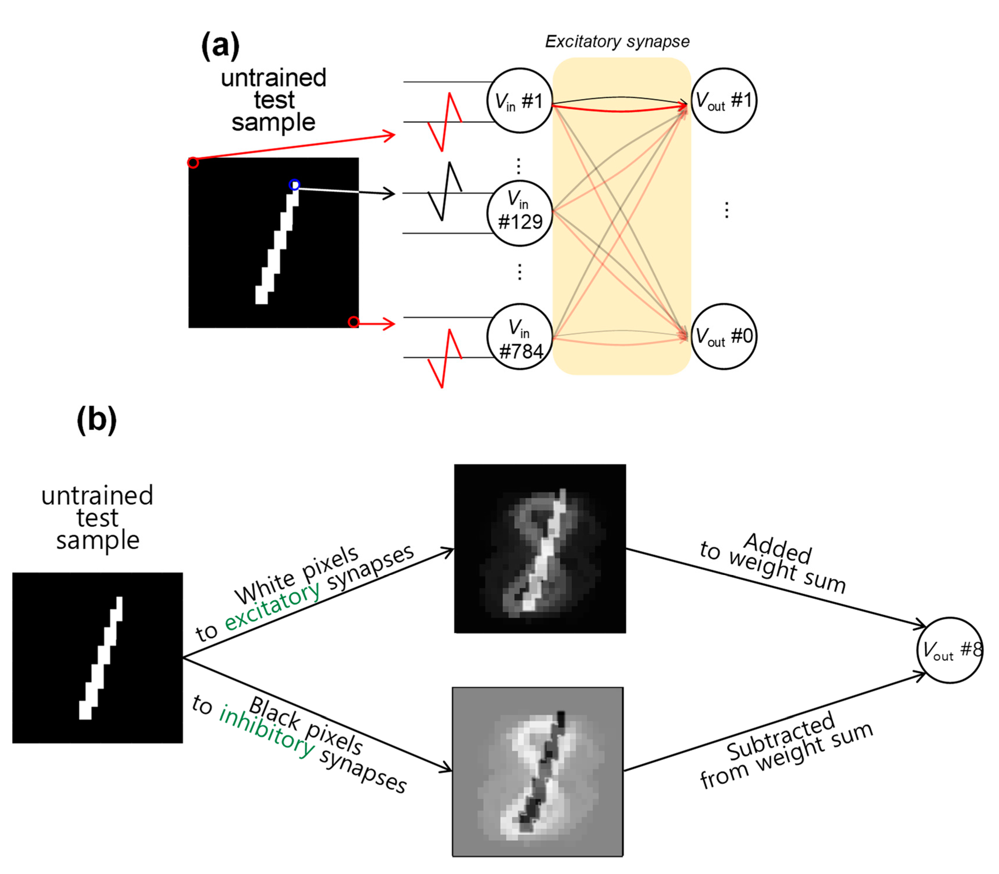
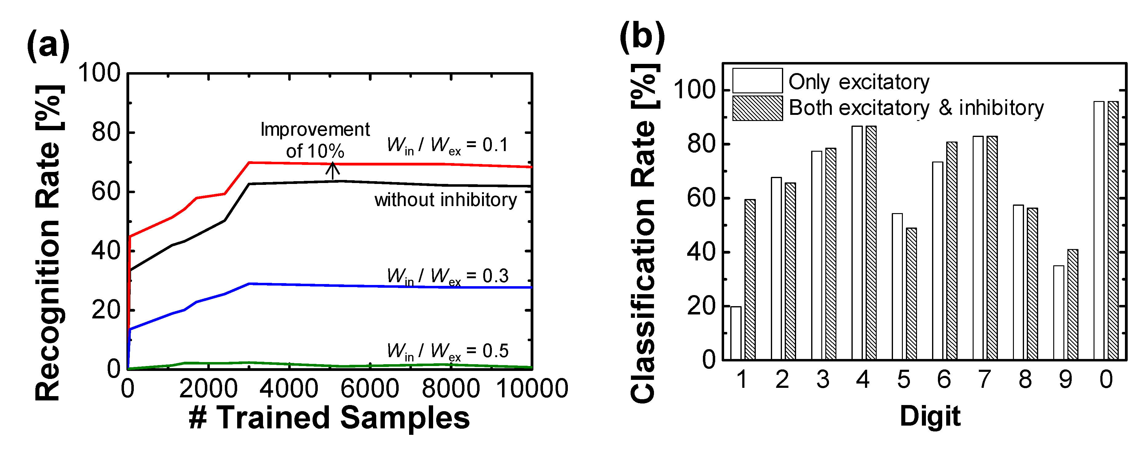
3. Results and Discussion
4. Conclusions
Author Contributions
Funding
Conflicts of Interest
References
- Backus, J. Can programming be liberated from the von Neumann style?: A functional style and its algebra of programs. Commun. ACM 1978, 21, 613–641. [Google Scholar] [CrossRef] [Green Version]
- Jeong, D.S.; Kim, K.M.; Kim, S.; Choi, B.J.; Hwang, C.S. Memristors for Energy-Efficient New Computing Paradigms. Adv. Electron. Mater. 2016, 2, 160090. [Google Scholar] [CrossRef]
- Merolla, P.A.; Arthur, J.V.; Alvarez-Icaza, R.; Cassidy, A.S.; Sawada, J.; Akopyan, F.; Jackson, B.L.; Imam, N.; Guo, C.; Nakamura, Y.; et al. A million spiking-neuron integrated circuit with a scalable communication network and interface. Science 2014, 345, 668–673. [Google Scholar] [CrossRef] [PubMed]
- Misra, J.; Saha, I. Artificial neural networks in hardware: A survey of two decades of progress. Neurocomputing 2010, 74, 239–255. [Google Scholar] [CrossRef]
- Maass, W. Networks of spiking neurons: The third generation of neural network models. Neural Netw. 1997, 10, 1659–1671. [Google Scholar] [CrossRef]
- Cohen, E.; Malka, D.; Shemer, A.; Shahmoon, A.; Zalevsky, Z.; London, M. Neural networks within multi-core optic fibers. Sci. Rep. 2016, 6, 29080. [Google Scholar] [CrossRef] [PubMed] [Green Version]
- Hwang, S.; Kim, H.; Park, J.; Kwon, M.-W.; Baek, M.-H.; Lee, J.-J.; Park, B.-G. System-level simulation of hardware spiking neural network based on synaptic transistors and I&F neuron circuits. IEEE Electron Device Lett. 2018, 39, 1441–1444. [Google Scholar]
- Seo, M.; Kang, M.-H.; Jeon, S.-B.; Bae, H.; Hur, J.; Jang, B.C.; Yun, S.; Cho, S.; Kim, W.-K.; Kim, M.-S.; et al. First demonstration of a logic-process compatible junctionless ferroelectric finfet synapse for neuromorphic applications. IEEE Electron Device Lett. 2018, 39, 1445–1448. [Google Scholar] [CrossRef]
- Park, Y.J.; Kwon, H.T.; Kim, B.; Lee, W.J.; Wee, D.H.; Choi, H.-S.; Park, B.-G.; Lee, J.-H.; Kim, Y. 3-D stacked synapse array based on charge-trap flash memory for implementation of deep neural networks. IEEE Trans. Electron Devices 2018, 66, 420–427. [Google Scholar] [CrossRef]
- Sung, C.; Lim, S.; Kim, H.; Kim, T.; Moon, K.; Song, J.; Kim, J.-J.; Hwang, H. Effect of conductance linearity and multi-level cell characteristics of TaOx-based synapse device on pattern recognition accuracy of neuromorphic system. Nanotechnology 2018, 29, 115203. [Google Scholar] [CrossRef]
- Kim, H.; Hwang, S.; Park, J.; Yun, S.; Lee, J.-H.; Park, B.-G. Spiking neural network using synaptic transistors and neuron circuits for pattern recognition with noisy images. IEEE Electron Device Lett. 2018, 39, 630–633. [Google Scholar] [CrossRef]
- Shabairou, N.; Cohen, E.; Wagner, O.; Malka, D.; Zalevsky, Z. Color image identification and reconstruction using artificial neural networks on multimode fiber images: Towards an all-optical design. Opt. Lett. 2018, 43, 5603–5606. [Google Scholar] [CrossRef] [PubMed]
- Truong, S.N.; Ham, S.-J.; Min, K.-S. Neuromorphic crossbar circuit with nanoscale filamentary-switching binary memristors for speech recognition. Nanoscale Res. Lett. 2014, 9, 629. [Google Scholar] [CrossRef] [PubMed] [Green Version]
- Prezioso, M.; Merrikh-Bayat, F.; Hoskins, B.; Adam, G.; Likharev, K.K.; Strukov, D.B. Training and operation of an integrated neuromorphic network based on metal-oxide memristors. Nature 2015, 521, 61–64. [Google Scholar] [CrossRef] [Green Version]
- Ambrogio, S.; Balatti, S.; Milo, V.; Carboni, R.; Wang, Z.-Q.; Calderoni, A.; Ramaswamy, N.; Ielmini, D. Neuromorphic learning and recognition with one-transistor-one-resistor synapses and bistable metal oxide RRAM. IEEE Trans. Electron Devices 2016, 63, 1508–1515. [Google Scholar] [CrossRef] [Green Version]
- Park, J.; Kwak, M.; Moon, K.; Woo, J.; Lee, D.; Hwang, H. TiOx-based RRAM synapse with 64-levels of conductance and symmetric conductance change by adopting a hybrid pulse scheme for neuromorphic computing. IEEE Electron Device Lett. 2016, 37, 1559–1562. [Google Scholar] [CrossRef]
- Kim, S.; Kim, H.; Hwang, S.; Kim, M.-H.; Chang, Y.-F.; Park, B.-G. Analog synaptic behavior of a silicon nitride memristor. ACS Appl. Mater. Interfaces 2017, 9, 40420–40427. [Google Scholar] [CrossRef]
- Kim, S.; Ishii, M.; Lewis, S.; Perri, T.; BrightSky, M.; Kim, W.; Jordan, R.; Burr, G.W.; Sosa, N.; Ray, A.; et al. NVM neuromorphic core with 64k-cell (256-by-256) phase change memory synaptic array with on-chip neuron circuits for continuous in-situ learning. In Proceedings of the 2012 International Electron Devices Meeting, San Francisco, CA, USA, 7−9 December 2012; pp. 443–446. [Google Scholar]
- Tuma, T.; Le-Gallo, M.; Sebastian, A.; Eleftheriou, E. detecting correlations using phase-change neurons and synapses. IEEE Electron Device Lett. 2016, 37, 1238–1241. [Google Scholar] [CrossRef]
- Kuzum, D.; Jeyasingh, R.G.; Lee, B.; Wong, H.-S.P. Nanoelectronic programmable synapses based on phase change materials for brain-inspired computing. Nano Lett. 2011, 12, 2179–2186. [Google Scholar] [CrossRef]
- Oh, S.; Kim, T.; Kwak, M.; Song, J.; Woo, J.; Jeon, S.; Yoo, I.K.; Hwang, H. HfZrOx-based ferroelectric synapse device with 32 levels of conductance states for neuromorphic applications. IEEE Electron Device Lett. 2017, 38, 732–735. [Google Scholar] [CrossRef]
- Mulaosmanovic, H.; Ocker, J.; Müller, S.; Noack, M.; Müller, J.; Polakowski, P.; Mikolajick, T.; Slesazeck, S. Novel ferroelectric FET based synapse for neuromorphic systems. In Proceedings of the 2017 Symposium on VLSI Technology, Kyoto, Japan, 5–8 June 2017; pp. T176–T177. [Google Scholar]
- Wang, J.; Li, Y.; Liang, R.; Zhang, Y.; Mao, W.; Yang, Y.; Ren, T.-L. Synaptic computation demonstrated in a two-synapse network based on top-gate electric-double-layer synaptic transistors. IEEE Electron Device Lett. 2017, 38, 1496–1499. [Google Scholar] [CrossRef]
- Wan, X.; Yang, Y.; Feng, P.; Shi, Y.; Wan, Q. Short-term plasticity and synaptic filtering emulated in electrolyte-gated IGZO transistors. IEEE Electron Device Lett. 2016, 37, 299–302. [Google Scholar] [CrossRef]
- Shi, J.; Ha, S.D.; Zhou, Y.; Schoofs, F.; Ramanathan, S. A correlated nickelate synaptic transistor. Nat. Commun. 2013, 4, 2676. [Google Scholar] [CrossRef] [PubMed] [Green Version]
- Kim, H.; Park, J.; Kwon, M.-W.; Lee, J.-H.; Park, B.-G. Silicon-based floating-body synaptic transistor with frequency dependent short-and long-term memories. IEEE Electron Device Lett. 2016, 37, 249–252. [Google Scholar] [CrossRef]
- Kim, H.; Cho, S.; Sun, M.-C.; Park, J.; Hwang, S.; Park, B.-G. Simulation study on silicon-based floating body synaptic transistor with short-and long-term memory functions and its spike timing-dependent plasticity. J. Semicond. Technol. Sci. 2016, 16, 657–663. [Google Scholar] [CrossRef] [Green Version]
- Kim, H.; Hwang, S.; Park, J.; Park, B.-G. Silicon synaptic transistor for hardware-based spiking neural network and neuromorphic system. Nanotechnology 2017, 28, 405202. [Google Scholar] [CrossRef]
- Kim, H.; Sun, M.-C.; Hwang, S.; Kim, H.-M.; Lee, J.-H.; Park, B.-G. Fabrication of asymmetric independent dual-gate FinFET using sidewall spacer patterning and CMP processes. Microelectron. Eng. 2018, 185, 29–34. [Google Scholar] [CrossRef]
- Kim, S.; Lee, S.-H.; Kim, Y.-G.; Cho, S.; Park, B.-G. Highly compact and accurate circuit-level macro modeling of gate-all-around charge-trap flash memory. Jpn. J. Appl. Phys. 2016, 56, 014302. [Google Scholar] [CrossRef]
- Sonoda, K.; Tanizawa, M.; Shimizu, S.; Araki, Y.; Kawai, S.; Ogura, T.; Kobayashi, S.; Ishikawa, K.; Eimori, T.; Inoue, Y.; et al. Compact modeling of a flash memory cell including substrate-bias-dependent hot-electron gate current. IEEE Trans. Electron Devices 2004, 51, 1726–1733. [Google Scholar] [CrossRef]
- Park, J.; Kwon, M.-W.; Kim, H.; Hwang, S.; Lee, J.-J.; Park, B.-G. Compact neuromorphic system with four-terminal si-based synaptic devices for spiking neural networks. IEEE Trans. Electron Devices 2017, 64, 2438–2444. [Google Scholar] [CrossRef]
- LeCun, Y.; Bengio, Y.; Hinton, G. Deep learning. Nature 2015, 521, 436–444. [Google Scholar] [CrossRef] [PubMed]
- Nair, V.; Hinton, G.E. Rectified linear units improve restricted boltzmann machines. In Proceedings of the 27th International Conference on Machine Learning, Haifa, Israel, 21–24 June 2010; pp. 807–814. [Google Scholar]
- Maas, A.L.; Hannun, A.Y.; Ng, A.Y. Rectifier nonlinearities improve neural network acoustic models. In Proceedings of the 30th International Conference on Machine Learning, Atlanta, GA, USA, 16–21 June 2013. [Google Scholar]
- Diehl, P.U.; Neil, D.; Binas, J.; Cook, M.; Liu, S.-C.; Pfeiffer, M. Fast-classifying, high-accuracy spiking deep networks through weight and threshold balancing. In Proceedings of the 2015 International Joint Conference on Neural Networks, Killarney, Ireland, 12–17 July 2015; pp. 1–8. [Google Scholar]


© 2019 by the authors. Licensee MDPI, Basel, Switzerland. This article is an open access article distributed under the terms and conditions of the Creative Commons Attribution (CC BY) license (http://creativecommons.org/licenses/by/4.0/).
Share and Cite
Kim, H.; Park, B.-G. Solving Overlapping Pattern Issues in On-Chip Learning of Bio-Inspired Neuromorphic System with Synaptic Transistors. Electronics 2020, 9, 13. https://doi.org/10.3390/electronics9010013
Kim H, Park B-G. Solving Overlapping Pattern Issues in On-Chip Learning of Bio-Inspired Neuromorphic System with Synaptic Transistors. Electronics. 2020; 9(1):13. https://doi.org/10.3390/electronics9010013
Chicago/Turabian StyleKim, Hyungjin, and Byung-Gook Park. 2020. "Solving Overlapping Pattern Issues in On-Chip Learning of Bio-Inspired Neuromorphic System with Synaptic Transistors" Electronics 9, no. 1: 13. https://doi.org/10.3390/electronics9010013
APA StyleKim, H., & Park, B.-G. (2020). Solving Overlapping Pattern Issues in On-Chip Learning of Bio-Inspired Neuromorphic System with Synaptic Transistors. Electronics, 9(1), 13. https://doi.org/10.3390/electronics9010013