Article

3-D Synapse Array Architecture Based on Charge-Trap Flash Memory for Neuromorphic Application

1
School of Electrical and Computer Engineering, University of Seoul, Seoul 02504, Korea
2
Applied Materials Korea, Ltd., Hwaseong-si, Gyeonggi-do 18364, Korea
3
Department of Electrical and Computer Engineering, Seoul National University, Seoul 08826, Korea
*
Author to whom correspondence should be addressed.
Electronics 2020, 9(1), 57; https://doi.org/10.3390/electronics9010057
Submission received: 29 November 2019 / Revised: 20 December 2019 / Accepted: 29 December 2019 / Published: 30 December 2019
(This article belongs to the Special Issue Semiconductor Memory Devices for Hardware-Driven Neuromorphic Systems)

Abstract

:
In order to address a fundamental bottleneck of conventional digital computers, there is recently a tremendous upsurge of investigations on hardware-based neuromorphic systems. To emulate the functionalities of artificial neural networks, various synaptic devices and their 2-D cross-point array structures have been proposed. In our previous work, we proposed the 3-D synapse array architecture based on a charge-trap flash (CTF) memory. It has the advantages of high-density integration of 3-D stacking technology and excellent reliability characteristics of mature CTF device technology. This paper examines some issues of the 3-D synapse array architecture. Also, we propose an improved structure and programming method compared to the previous work. The synaptic characteristics of the proposed method are closely examined and validated through a technology computer-aided design (TCAD) device simulation and a system-level simulation for the pattern recognition task. The proposed technology will be the promising solution for high-performance and high-reliability of neuromorphic hardware systems.

1. Introduction

Neuromorphic systems have been attracting much attention for next-generation computing systems to overcome the von Neumann architecture [1,2,3,4,5]. The term “neuromorphic” refers to an artificial neural system that mimics neurons and synapses of the biological nervous system [3]. A neuron generates a spike when a membrane potential which is the result of the spatial and temporal summation of the signal received from the pre-neuron exceeds a threshold, and the generated spike is transmitted to the post-neuron. A synapse refers to the junction between neurons, and each synapse has its own synaptic weight which is the connection strength between neurons [6]. In a neuromorphic system, synaptic weight can be represented by the conductance of synapse device.
The requirements of a synapse device to implement a neuromorphic system are as follows: small cell size, low-energy consumption, multi-level operations, symmetric and linear weight change, high endurance and complementary metal-oxide semiconductor (CMOS) compatibility [5]. Various memory devices, such as static random-access memories (SRAM) [7], resistive random-access memories (RRAM) [8], phase change memories (PCM) [9], floating gate- memories (FG-memory) [10] and charge-trap flash memories [11] have been proposed to implement the synapse operation. Among them, charge-trap flash (CTF) devices have good CMOS compatibility and excellent reliability [12,13,14,15].
In our previous work, we proposed a 3-D stacked synapse array based on a charge trap flash (CTF) device [11]. Three-dimensional stacking technology is currently used in the commercialized Not AND (NAND) flash memory products for ultra-high density [14]. Similarly, a 3-D stacked synapse array has the advantage of chip-size reduction when implementing very-large-size artificial neural networks. Consequently, it has the potential to be a promising technology for implementing neuromorphic hardware systems. For the design of the 3-D stacked synapse array architecture, there are several issues. At the full array level, how to operate each layer selectively and how to efficiently form the metal interconnects with peripheral circuits are critical issues. At the device level, how to implement accurate synaptic weight levels with low energy consumption is an important issue. Especially, linear and symmetric synaptic weight (conductance) modulations are essential to improve the accuracy of neuromorphic hardware systems [1,2,3,4].
In this paper, we examine these issues and suggest two improvements in terms of an architecture design and a device operation method. The rest of the paper is structured as follows: Section 2 contains design methods based on the viewpoint of a full-chip architecture. In this section, we review the 3-D stacked synapse array structure developed in the previous work [11] and propose an improved version of the 3-D stacked synapse array architecture to solve the unwanted problem of the previous version. In Section 3, we propose an improved programming method to obtain linear and symmetric conductance changes. Using a pattern recognition application with the Modified National Institute of Standards and Technology (MNIST) database, we demonstrate the improvement of the proposed method.

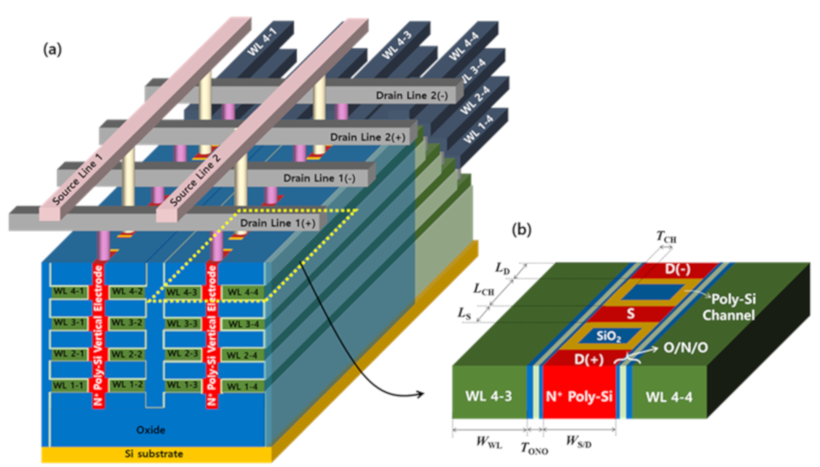
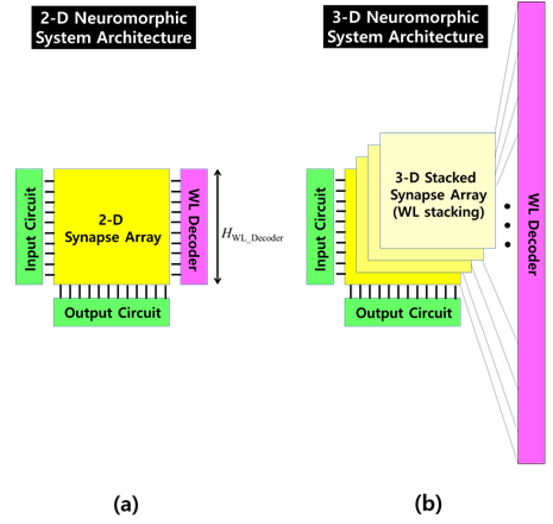
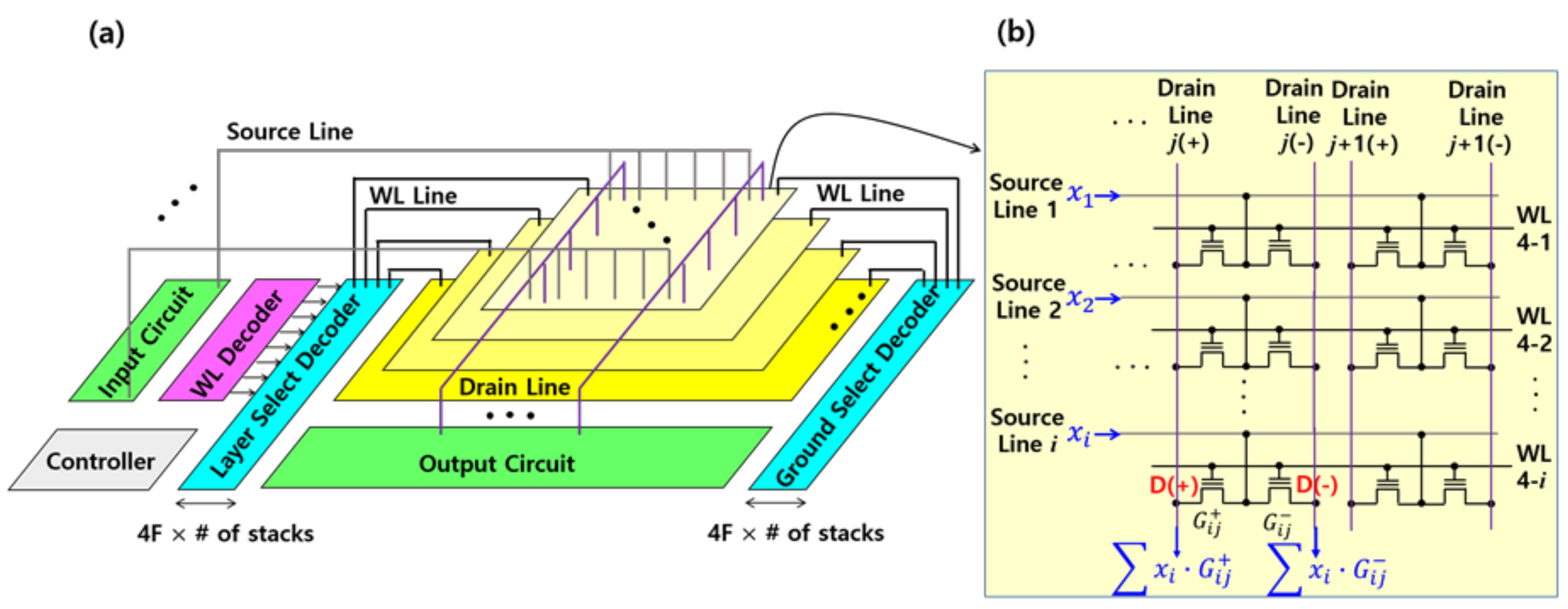
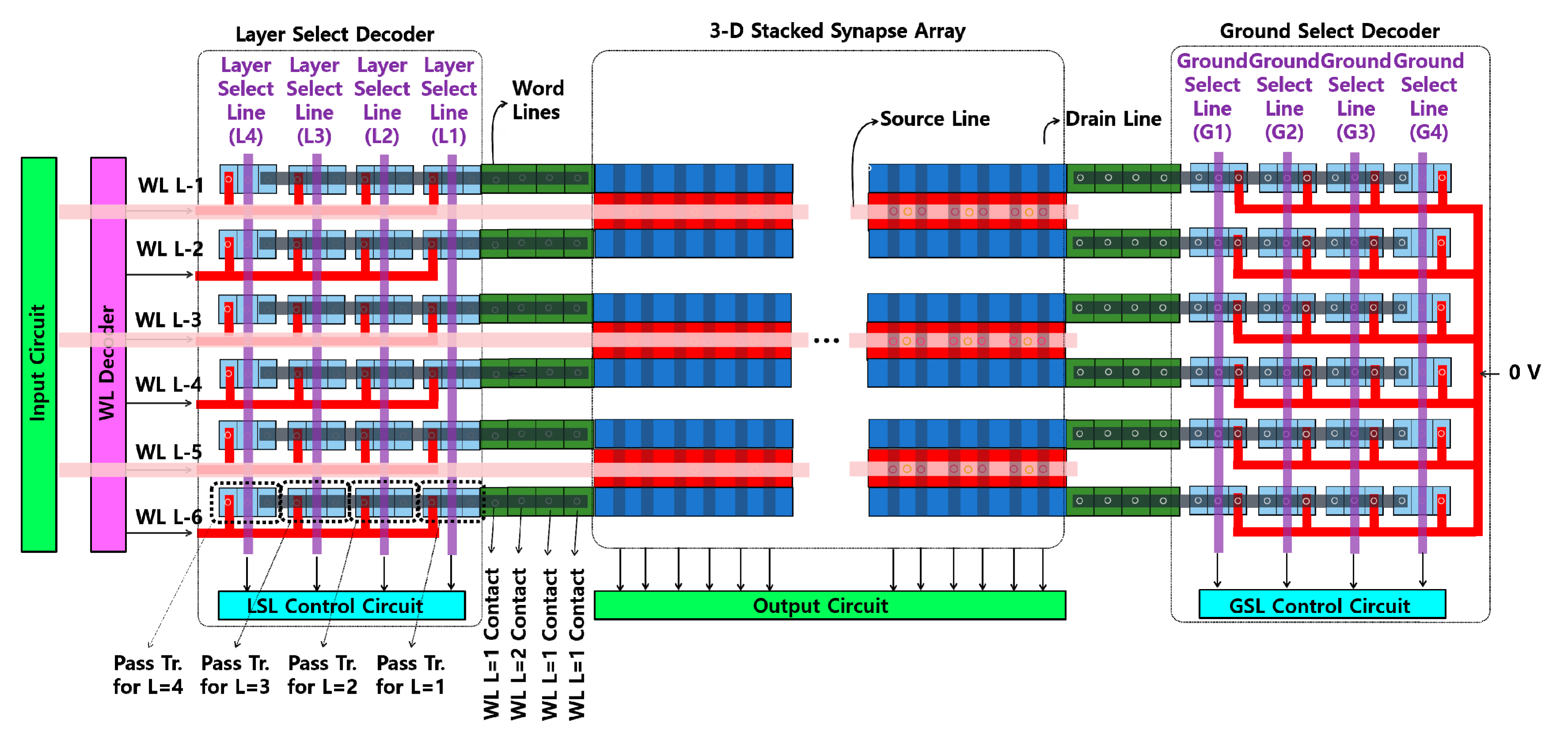
2. Design Methods of 3-D Synapse Array Architecture

In general, a large-size artificial neural network that has a large number of synaptic weights and neuron layers is required to obtain high performance artificial intelligence tasks. In the case of the ImageNet classification challenge, state-of-the-art deep neural network (DNN) architectures have 5~155M synaptic weight parameters [16]. In order to implement efficiently a large-size artificial neural network on a limited-size hardware chip, we proposed the 3-D stacked synapse array structure (Figure 1) in the previous work [11].
Unit synapse cell is composed of two CTF devices having two drain nodes (D(+), D(−)) and common source node(S). The D(+) part is connected to the output neuron circuit to increase membrane potential, acting as an excitatory synaptic behavior. The D(−) part is connected to the output neuron circuit to decrease membrane potential, acting as an inhibitory synaptic behavior. By using this configuration, it can be represented the negative and positive weight at the same time. As summarized in Table 1, the CTF device has several advantages over other non-volatile memory devices. First, it does not need an additional selector device because the three-terminal MOSFET-based unit cell has a built-in selection operation. Second, it has perfect CMOS compatibility. Third, the linear and incremental modulation of the weight (conductance) can be more easily achieved because its conductance is determined by the number of trapped charges. Fourth, it has good retention reliability characteristics. On the other hand, the drawback of CTF is large power consumption during program operation. Therefore, CTF devices are the best solution for off-chip learning-based neuromorphic systems where frequent weight updates do not occur.
The proposed 3-D stacked synapse array structure is based on the word-line stacking method which is similar to the commercialized V-NAND flash memory. Therefore, it has the advantage of utilizing the existing stable process methods used in V-NAND flash memory.
A key issue in the design of 3-D stacked synapse array architecture is the metal interconnection. For example, a 4-layer stacked synapse array would have four times as many word lines as a 2-D synapse array. If the word-line (WL) decoder is connected by a conventional metal interconnection method, the vertical length of the WL decoder (HWL_Decoder) will increase as illustrated in Figure 2, resulting in an enormous loss of area efficiency in terms of full-chip level architecture. To solve this issue, we proposed the smart design of a layer select decoder with 3-D metal line connection in the previous work [11]. As shown in Figure 3a, the area of WL decoder is not increased, and a layer select decoder is added to selectively operate each stacked layer. A layer select decoder delivers the gate voltages generated by the WL decoder to the WLs of the selected layer. It is important to note that the vertical length of a layer select decoder is the same as that of the WL decode, and the horizontal length is only 4 F×N where F is the minimum feature size and N is the number of staked layers. The specific structure of the transistors and metal interconnects is depicted in our previous paper [11].
The top-view layout of the 3-D synapse array architecture is illustrated in Figure 4. The layer select decoder is composed of pass transistors. The pass transistors are arranged next to each word line and are connected one-to-one with each WL contact. The gate nodes of the pass transistors are vertically connected to form a layer select line (LSL) that is controlled by LSL control circuit. Through this configuration, each stacked layer can be selectively operated while maintaining compact full-chip configuration efficiency. For example, if the turn-on voltage is applied to L4 and the turn-off voltages are applied to L1~L3, pass transistors corresponding to L = 4 are activated. Consequently, the WL voltages generated in the WL decoder are transferred to the forth-layer WLs (L = 4).
In this paper, we proposed an improved architecture design compared to the previous work, adding the ground select decoder as shown in Figure 4. If there is only a layer select decoder, the WLs of the unselected stacked layer are on a floating state because they are not connected to the WL decoder. In this case, the potential of the WLs of the unselected layer varies due to the capacitive coupling between the stacked WLs. In the worst case, the WLs of unselected layers located above or below (L = n − 1 or L = n + 1) the selected layer (L = n) may be boosted together when a high voltage is applied to the selected WLs. To solve this inherent risk of the architecture of the previous version, a ground select decoder that applies a turn-off voltage (0 V) to the WLs of the unselected layer is added to the right side of the main 3-D stacked synapse array as shown in Figure 4.
The detailed manufacturing process of the 3-D synapse array was described in our previous paper [11]. The revised synapse array architecture can be made with the same process method. Since the newly added ground select decoder structure has the same structure as the layer select decoder, it can be made by just adding the same layout as the layer select decoder.
To validate the synaptic operations of the designed CTF-based synapse device, the technology computer-aided design (TCAD) device simulation (Synopsys Sentaurus [17]) was used. The specific device parameters are summarized in Table 2. Electrical characteristics of the designed synapse device are discussed in the next chapter.

3. Results

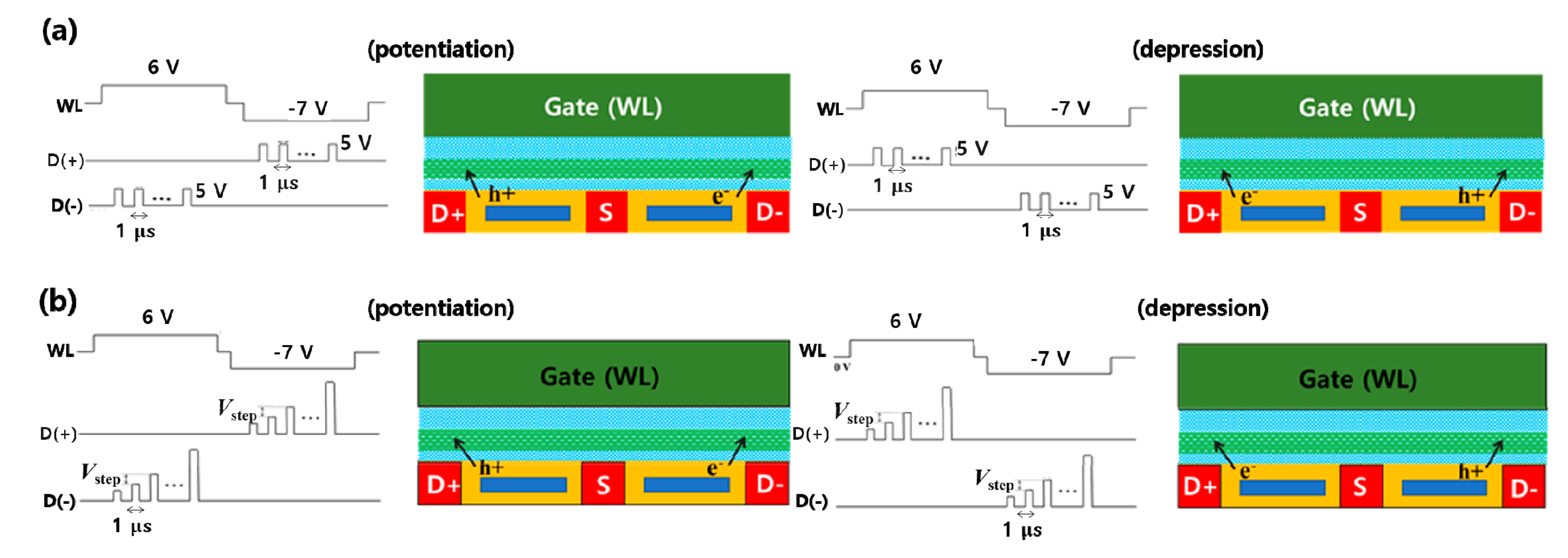
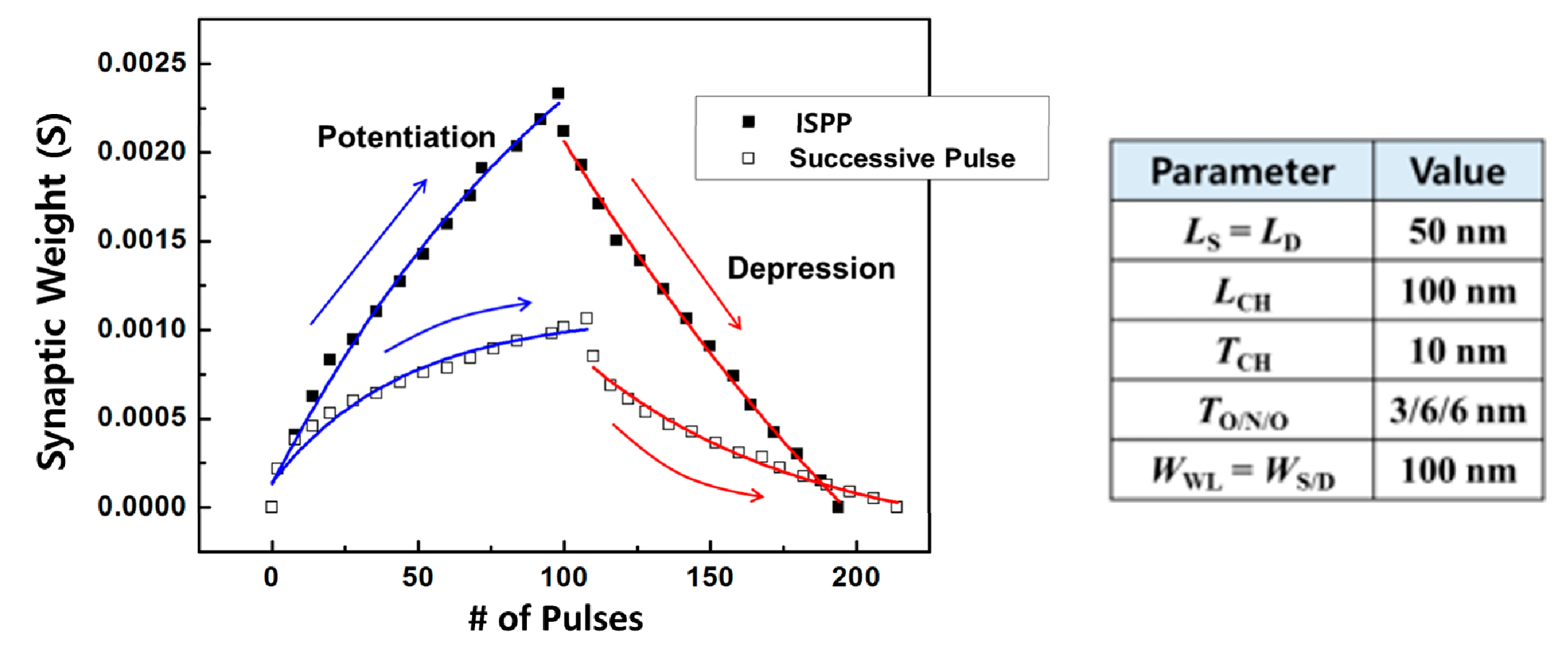
3.1. Synapse Device Operation

In the proposed synapse array (Figure 3b), synaptic weight (wij) of the artificial neural network is represented as follows:
wij = G+ijGij.
As depicted in Figure 3b, G+ij and Gij are the conductances of the D(+) CTF device and D(−) CTF device, respectively. Each conductance is determined by the amount of trapped charge in each charge-trap layer (silicon nitride). For the conductance modulation, hot-electron injection (HEI) and hot-hole injection (HHI) can be used as a charge injection mechanism. The potentiation process of increasing the synaptic weight can be performed by increasing G+ij and decreasing Gij. On the other hand, the depression process of decreasing the synaptic weight can be carried out by decreasing G+ij and increasing Gij. Using a technology computer-aided design (TCAD) device simulation (Synopsys Sentaurus), we verify two pulse schemes for the modulation of synaptic weight. A successive-pulse programming scheme and the incremental-step-pulse programming (ISPP) scheme are illustrated in Figure 5a,b, respectively.
A successive-pulse programming is a method of continuously applying drain pulses with the same voltage as shown in Figure 5a. In this programming scheme, the amount of conductance change is controlled by the number of applied drain pulses. When the drain pulse is applied, the sign of the gate voltage determines whether HEI or HHI occurs. If the drain pulse is applied when the gate bias is positive (6 V), HEI occurs. In this case, the threshold voltage increases by the trapped electron and the conductance decreases. On the other hand, if the drain pulse is applied when the gate bias in negative (−7 V), HHI occurs. In this case, the threshold voltage decreases by the trapped hole and the conductance increases. The proposed unit synapse cell is composed of two CTF devices. Consequently, the potentiation operation is conducted simultaneously by HHI in the D(+) CTF device and HEI in the D(−) CTF device. The depression operation is conducted by HEI in the D(+) device and HHI in the D(−) device.
The ISPP is used for the program scheme of NAND flash memory [18]. The program pulse is increased by a constant value Vstep after each program step, as shown in Figure 5b. In our previous paper, only successive-pulse programming was used. In this work, we applied the ISPP method to the conductance modulation of our designed synapse device. Using a TCAD device simulation, we compared the conductance modulation characteristics of successive-pulse programming and the ISPP. As shown in Figure 6, the ISPP scheme shows better synaptic behavior than the successive-pulse scheme. The ISPP scheme showed that the conductance changes linearly according to the number of applied pulses. Also, the range of available synaptic weights (memory window) can be further increased. Consequently, the ISPP scheme can adjust the synaptic weight more accurately than the successive-pulse programming scheme during the learning process. However, the ISPP scheme also has a drawback. In order to determine the start pulse voltage, a verify operation is required prior to programming to check the current synaptic weight value. Therefore, the ISPP scheme can increase the accuracy of the learning process, but also increases time and energy consumption.

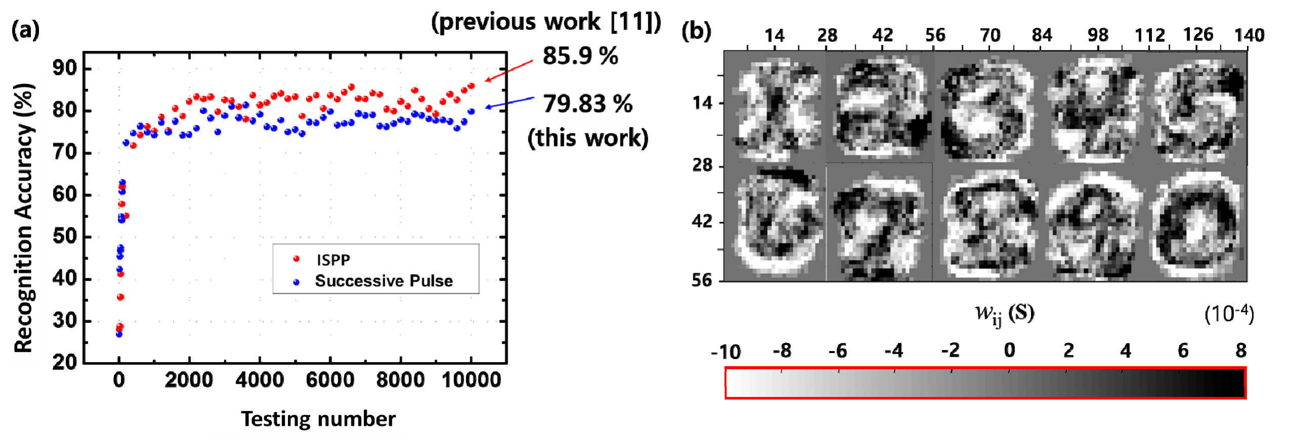
3.2. System-Level Simulation for Pattern Recognition
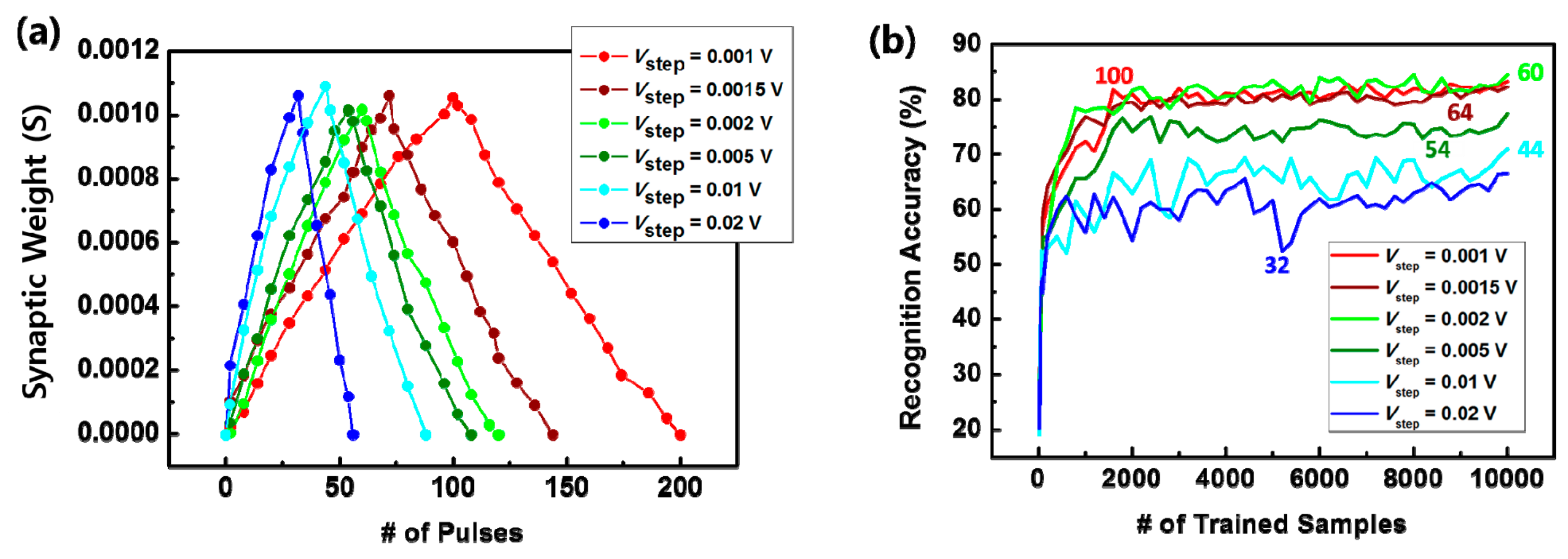
To validate the functionality of the proposed programming schemes, the single-layer artificial neural network system for the Modified National Institute of Standards and Technology (MNIST) pattern recognition was simulated. The MNIST database is a large database of handwritten digits, which contains about 60,000 learning images and 10,000 test images [19]. A total of 784 input neurons represent 28 × 28 pixels of each image and 10 output neurons represent 10 digits (0 ~ 9). We also used a rectifier linear unit (ReLU) as an activation function of neuron, which is one of the popular activation functions [20]. For the learning process, a supervised learning method was used. At first, the error was calculated at the output neurons. Next, the target change in synaptic weight (the number of programming pulses) was determined by the gradient descent method. After that, the synaptic weight value is updated based on fitted equations for the conductance modulation characteristics of a successive-pulse programming scheme and the ISPP scheme.
Figure 7a shows the system-level simulation result of the pattern recognition accuracy with the 10,000 test image samples. Compared to our previous work [11], the ISPP scheme can increase recognition accuracy by about 6% (a successive-pulse programming scheme in our previous work: 79.83% [11], and the ISPP scheme in this work: 85.9%). This result is in good agreement with the other papers that the linear conductance modulation characteristic is essential for the better performance of neuromorphic systems [5,21]. The synaptic weight maps after training 10,000 samples with the ISPP scheme are illustrated in Figure 7b.
In addition, we examined the synaptic weight modulation characteristics according to the various values of Vstep in the ISPP scheme. As illustrated in Figure 8a, a smaller Vstep allows for fine conductance modulation, which means that the number of the synaptic weight level can be increased. As a result, the fine conductance modulation ability with a smaller Vstep can obtain more accurate pattern recognition rate, as shown in Figure 8b. It should be noted, however, that the retention characteristics (the ability to distinguish each level for a long time) can deteriorate when the interval between each synaptic weight level becomes narrow. Therefore, the magnitude of Vstep should be determined considering the trade-off relationship between the retention characteristic and the accuracy.

4. Discussion

Currently, numerous researches based on different types of nonvolatile memory devices have been conducted to implement neuromorphic hardware systems. Table 3 summarizes some of the research results.
Almost all previous studies are based on the 2-D synapse array structure, but for the first time we proposed the 3-D stacked synapse array structure. This paper has addressed several issues associated with the design of the 3-D synapse array architecture in terms of a full-chip level. This will be an important guideline for designing a 3-D stacked synapse array. The approach of stacking CTF devices is a mature technology that has been already used in commercialized 3-D NAND flash memories. Consequently, the proposed 3-D synapse architecture is expected to have a high possibility of actual mass production. Also, it can achieve excellent reliability by utilizing the various technologies used in NAND flash memory. For example, we have demonstrated that the ISPP method can improve the pattern recognition accuracy of a neuromorphic system.
For future work, we will demonstrate the superiority of the proposed 3-D synapse architecture based on an actual fabricated array. In addition, application researches to various artificial neural networks such as a convolutional neural network (CNN) and a recurrent neural network (RNN) will be a crucial topic.

5. Conclusions

We proposed a 3-D synapse array architecture based on a CTF memory device. To resolve the drawback of the previous version of the architecture, a ground select decoder was newly added. Also, we introduced the ISPP scheme to improve the linearity of the conductance modulation. The characteristics of synaptic weight modulation was characterized using a TCAD device simulation. In addition, we demonstrated the feasibility of the proposed architecture for neuromorphic system applications through a MATLAB simulation for the MNIST pattern recognition. The proposed 3-D synapse array architecture that exhibits a compact chip configuration and a high-integration ability will be a promising technology that can realize hardware-based neuromorphic systems.

Author Contributions

H.-S.C. and Y.K. designed the architecture design and wrote the manuscript. Y.J.P. performed the device simulations. Y.K. confirmed the validities of the designed architecture and simulated synaptic operation. J.-H.L. conceived and developed the various types of 3-D synapse structures, initiated the overall research project. All authors have read and agreed to the published version of the manuscript.

Funding

This work was supported by the 2019 Research Fund of the University of Seoul for Yoon Kim. Also, this work was supported by the MOTIE (Ministry of Trade, Industry & Energy (10080583) and KSRC (Korea Semiconductor Research Consortium) support program for the development of the future semiconductor device for Jong-Ho Lee.

Conflicts of Interest

The authors declare no conflict of interest.

References

  1. Yu, S.; Gao, B.; Fang, Z.; Yu, H.; Kang, J.; Wong, H.S. A low energy oxide-based electronic synaptic device for neuromorphic visual systems with tolerance to device variation. Adv. Mater. 2013, 25, 1774–1779. [Google Scholar] [CrossRef] [PubMed]
  2. Liu, X.; Mao, M.; Liu, B.; Li, H.; Chen, Y.; Li, B.; Wang, Y.; Jiang, H.; Barnell, M.; Wu, Q.; et al. RENO: A high-efficient reconfigurable neuromorphic computing accelerator design. In Proceedings of the 2015 52nd ACM/EDAC/IEEE Design Automation Conference (DAC), San Francisco, CA, USA, 8–12 June 2015; pp. 1–6. [Google Scholar]
  3. Mead, C. Neuromorphic electronic systems. Proc. IEEE 1990, 78, 1629–1636. [Google Scholar] [CrossRef] [Green Version]
  4. Burr, G.W.; Shelby, R.M.; Sebastian, A.; Kim, S.; Kim, S.; Sidler, S.; Virwani, K.; Ishii, M.; Narayanan, P.; Fumarola, A.; et al. Neuromorphic computing using non-volatile memory. Adv. Phys. X 2016, 2, 89–124. [Google Scholar] [CrossRef]
  5. Choi, H.S.; Wee, D.H.; Kim, H.; Kim, S.; Ryoo, K.C.; Park, B.G.; Kim, Y. 3-D Floating-Gate Synapse Array with Spike-Time-Dependent Plasticity. IEEE Trans. Electron. Devices 2018, 65, 101–107. [Google Scholar] [CrossRef]
  6. Roberts, P.D.; Bell, C.C. Spike timing dependent synaptic plasticity in biological systems. Biol. Cybern. 2002, 87, 392–403. [Google Scholar] [CrossRef] [PubMed]
  7. Akopyan, F.; Sawada, J.; Cassidy, A.; Alvarez-Icaza, R.; Arthur, J.; Merolla, P.; Imam, N.; Nakamura, Y.; Datta, P.; Nam, G.J.; et al. Truenorth: Design and tool flow of a 65 mW 1 million neuron programmable neurosynaptic chip. IEEE Trans. Comput. Aided Des. Integr. Circuits Syst. 2015, 34, 1537–1557. [Google Scholar] [CrossRef]
  8. Yu, S.; Wu, Y.; Jeyasingh, R.; Kuzum, D.; Wong, H.S. An Electronic Synapse Device Based on Metal Oxide Resistive Switching Memory for Neuromorphic Computation. IEEE Trans. Electron. Devices 2011, 58, 2729–2737. [Google Scholar] [CrossRef]
  9. Panwar, N.; Kumar, D.; Upadhyay, N.K.; Arya, P.; Ganguly, U.; Rajendran, B. Memristive synaptic plasticity in Pr0.7Ca0.3MnO3 RRAM by bio-mimetic programming. In Proceedings of the 72nd Device Research Conference, Santa Barbara, CA, USA, 22–25 June 2014; pp. 135–136. [Google Scholar]
  10. Diorio, C.; Hasler, P.; Minch, B.A.; Mead, C.A. A floating-gate MOS learning array with locally computed weight updates. IEEE Trans. Electron. Devices 1997, 44, 2281–2289. [Google Scholar] [CrossRef] [Green Version]
  11. Park, Y.J.; Kwon, H.T.; Kim, B.; Lee, W.J.; Wee, D.H.; Choi, H.S.; Park, B.G.; Lee, J.H.; Kim, Y. 3-D Stacked Synapse Array Based on Charge-Trap Flash Memory for Implementation of Deep Neural Networks. IEEE Trans. Electron. Devices 2019, 66, 420–427. [Google Scholar] [CrossRef]
  12. Lee, J.; Park, B.G.; Kim, Y. Implementation of Boolean Logic Functions in Charge Trap Flash for In-Memory Computing. IEEE Electron. Device Lett. 2019, 40, 1358–1361. [Google Scholar] [CrossRef]
  13. Kim, Y.; Kang, M. Down-coupling phenomenon of floating channel in 3D NAND flash memory. IEEE Electron. Device Lett. 2016, 37, 1566–1569. [Google Scholar] [CrossRef]
  14. Jeong, W.; Im, J.W.; Kim, D.H.; Nam, S.W.; Shim, D.K.; Choi, M.H.; Yoon, H.J.; Kim, D.H.; Kim, Y.S.; Park, H.W.; et al. A 128 Gb 3b/cell V-NAND flash memory with 1 Gb/s I/O rate. IEEE J. Solid-State Circuits 2016, 51, 204–212. [Google Scholar]
  15. Kang, M.; Kim, Y. Natural Local Self-Boosting Effect in 3D NAND Flash Memory. IEEE Electron. Device Lett. 2017, 38, 1236–1239. [Google Scholar] [CrossRef]
  16. Canziani, A.; Paszke, A.; Culurciello, E. An Analysis of Deep Neural Network Models for Practical Applications. arXiv 2017, arXiv:1605.07678. [Google Scholar]
  17. Sentaurus Device User Guide; Ver. I-2013.12; Synopsys: Mountain View, CA, USA, 2012.
  18. Kim, Y.; Seo, J.Y.; Lee, S.H.; Park, B.G. A New Programming Method to Alleviate the Program Speed Variation in Three-Dimensional Stacked Array NAND Flash Memory. JSTS 2014, 5, 566–571. [Google Scholar] [CrossRef] [Green Version]
  19. LeCun, Y.; Bottou, L.; Bengio, Y.; Haffner, P. Gradient-based learning applied to document recognition. Proc. IEEE 1998, 86, 2278–2324. [Google Scholar] [CrossRef] [Green Version]
  20. Nair, V.; Hinton, G.E. Rectified linear units improve restricted Boltzmann machines. In Proceedings of the 27th International Conference on Machine Learning (ICML-10), Haifa, Israel, 21–24 June 2010; pp. 807–814. [Google Scholar]
  21. Burr, G.W.; Shelby, R.M.; Sidler, S.; Di Nolfo, C.; Jang, J.; Boybat, I.; Shenoy, R.S.; Narayanan, P.; Virwani, K.; Giacometti, E.U.; et al. Experimental Demonstration and Tolerancing of a Large-Scale Neural Network (165000 Synapses) Using Phase-Change Memory as the Synaptic Weight Element. IEEE Trans. Electron. Devices 2015, 62, 3498–3507. [Google Scholar] [CrossRef]
  22. Kim, H.; Hwang, S.; Park, J.; Park, B.G. Silicon synaptic transistor for hardware-based spiking neural network and neuromorphic system. Nanotechnology 2017, 28, 405202. [Google Scholar] [CrossRef] [PubMed]
  23. Kim, S.; Kim, H.; Hwang, S.; Kim, M.H.; Chang, Y.F.; Park, B.G. Analog Synaptic Behavior of a Silicon Nitride Memristor. ACS Appl. Mater. Interfaces 2017, 9, 40420–40427. [Google Scholar] [CrossRef] [PubMed]
  24. Ambrogio, S.; Ciocchini, N.; Laudato, M.; Milo, V.; Pirovano, A.; Fantini, P.; Ielmini, D. Unsupervised learning by spike timing dependent plasticity in phase change memory (PCM) synapses. Front. Neurosci. 2016, 10, 56. [Google Scholar] [CrossRef] [PubMed] [Green Version]
Figure 1. 3-D synapse array structure [11]. (a) 3-D stacked synapse device; (b) Unit synapse cell structure.
Electronics 09 00057 g001
Figure 2. Metal interconnection scheme of synapse array architecture. (a) 2-D neuromorphic system architecture; (b) 3-D neuromorphic system architecture (a bad design example).
Electronics 09 00057 g002
Figure 3. Schematic of the proposed 3-D synapse array architecture. (a) Metal interconnection of a full-chip architecture; (b) Each synapse layer configuration to implement artificial neural network.
Electronics 09 00057 g003
Figure 4. Top view image of the revised synapse array architecture.
Electronics 09 00057 g004
Figure 5. Programming schemes for synaptic weight (conductance). (a) Successive-pulse programming scheme; (b) Incremental-step-pulse programming scheme.
Electronics 09 00057 g005
Figure 6. Gradual changes of synaptic weights by successive-pulse programming and incremental-step-pulse programming (ISPP).
Electronics 09 00057 g006
Figure 7. Modified National Institute of Standards and Technology (MNIST) pattern recognition result. (a) Recognition accuracy comparison between a successive-pulse programming and the ISPP; (b) Synaptic weight map after training 10,000 samples with the ISPP scheme.
Electronics 09 00057 g007
Figure 8. MNIST pattern recognition result by using the ISPP scheme. (a) The gradual conductance change by applying various Vstep; (b) Recognition accuracy as a function of the training samples for the various Vstep. The number means the weight levels (maximum pulse number).
Electronics 09 00057 g008
Table 1. Comparison between non-volatile memory devices for neuromorphic hardware systems.
RRAMPCMSTT-MRAMCTF
Device Structure2 terminals2 terminals2 terminals3 terminals
Selectorneededneededneededunneeded
Cell Size4 ~ 12 F24 ~ 12 F26 ~ 20 F24 ~ 8 F2
CMOS Compatibilitygoodgoodmoderatevery good
Multi-Level Operationgoodgoodmoderatevery good
Weight Changeabrupt SETabrupt RESETstochastic changegood symmetric
Write Latency20 ~ 100 ns40 ~ 150 ns2 ~ 20 ns>1 μs
Write Energylowmidlowmid~high
Retentionmoderategoodgoodvery good
Table 2. Physical parameters of the device used for electrical simulation.
Value
LS = LD50 nm
LCH100 nm
TCH10 nm
TO/N/O3/6/6 nm
WWL = WS/D100 nm
Table 3. Comparison between several research results of neuromorphic applications.
This WorkPrevious Work [11][22][23][24]
Synapse DeviceCTFCTFCTFRRAMPRAM
Array Architecture3-D array3-D array2-D array2-D array2-D array
Neuron Layersingle-layersingle-layersingle-layersingle-layermulti-layer
Learning Typesupervisedsupervisedsupervisedsupervisedunsupervised
Recognition Rate85.9%79.8%84%87.9%95.5%
Result Typesimulationsimulationmeasurementmeasurementsimulation

