Article

Analytical Current-Voltage Model for Gate-All-Around Transistor with Poly-Crystalline Silicon Channel

Department of Electronics Engineering, Konkuk University, Seoul 143701, Korea
*
Author to whom correspondence should be addressed.
Electronics 2019, 8(9), 988; https://doi.org/10.3390/electronics8090988
Submission received: 12 August 2019 / Revised: 29 August 2019 / Accepted: 31 August 2019 / Published: 4 September 2019
(This article belongs to the Special Issue New CMOS Devices and Their Applications)

Abstract

:
Poly-crystalline silicon channel transistors have been used as a display TFT for a long time and have recently been used in a 3D vertical NAND Flash which is a transistor with 2D plane NAND upright. In addition, multi-gate transistors such as FinFETs and a gate-all-around (GAA) structure has been used to suppress the short-channel effects for logic/analog and memory applications. Compact models for poly-crystalline silicon (poly-silicon) channel planar TFTs and single crystalline silicon channel GAA MOSFETs have been developed separately, however, there are few models consider these two physics at the same time. In this work, we derived new analytical current-voltage model for GAA transistor with poly-silicon channel by considering the cylindrical coordinates and the grain boundary effect. Based on the derived formula, the compact I-V model for various operating regions and threshold voltage was proposed for the first time. The proposed model was compared with the measured data and good agreements were observed.

1. Introduction

With growing technology, compact and faster semiconductor transistors are required. To achieve this, the channel length of a device was reduced. However, as the channel length is reduced to a nanoscale region, the performance of the scaled down devices is degraded by the short-channel effects [1,2]. To avoid short-channel effects, there have been many studies on multi-gate transistors such as FinFETs and gate-all-around (GAA) MOSFETs. The common feature of these structures is that the gate surrounds the channel. In addition, in display application, poly-silicon has a faster electron field-effect mobility speed than a-Si, TFTs using poly-silicon have been used instead of a-Si TFTs [3]. Moreover, in a memory application pursuing the rapid integration density path of the floating gate beyond 20 nm, 3D NAND device has been adopted as the next generation solution. Majority of the solutions presented recently use a deposited poly-silicon channel [4]. Meanwhile, many studies have been conducted on compact modeling of GAA MOSFETs [5,6,7] and polysilicon channel MOSFETs [8,9,10], respectively. The existing GAA MOSFETs papers considered cylindrical coordinates according to the device structure. Compact modeling was performed but using single-crystalline silicon and grain boundary effect which is represent using poly-silicon was not considered at all. Similarly, the existing poly-silicon TFTs papers considered the grain boundary effect by using poly-silicon. Although compact modeling was performed, cylindrical coordinates was not considered since the device is planar TFTs structure. However, there is only one published paper considering cylindrical coordinates and grain boundary effect. In Fei Yu’s studies [11], which modeled the I-V characteristics through the Lambert-W function and some approximation techniques, the surface potential of poly-silicon GAA transistors have been studied. However, the result of the model is not intuitive to implement SPICE simulation because of the complexity of the Equation and to understand the device operation and major electrical characteristics (e.g. threshold voltage) per operating domain. This issue is most often attributed to the use of GAA’s cylindrical coordinates and additional trap charge at the grain boundary in a poly-silicon channel. In this work, to solve this issue, by using proper approximations for each operating region like as D. Jimenez's work [12] we propose analytical simple drain current and threshold voltage model which can give useful and intuitive Equation for poly-Si GAA transistor.

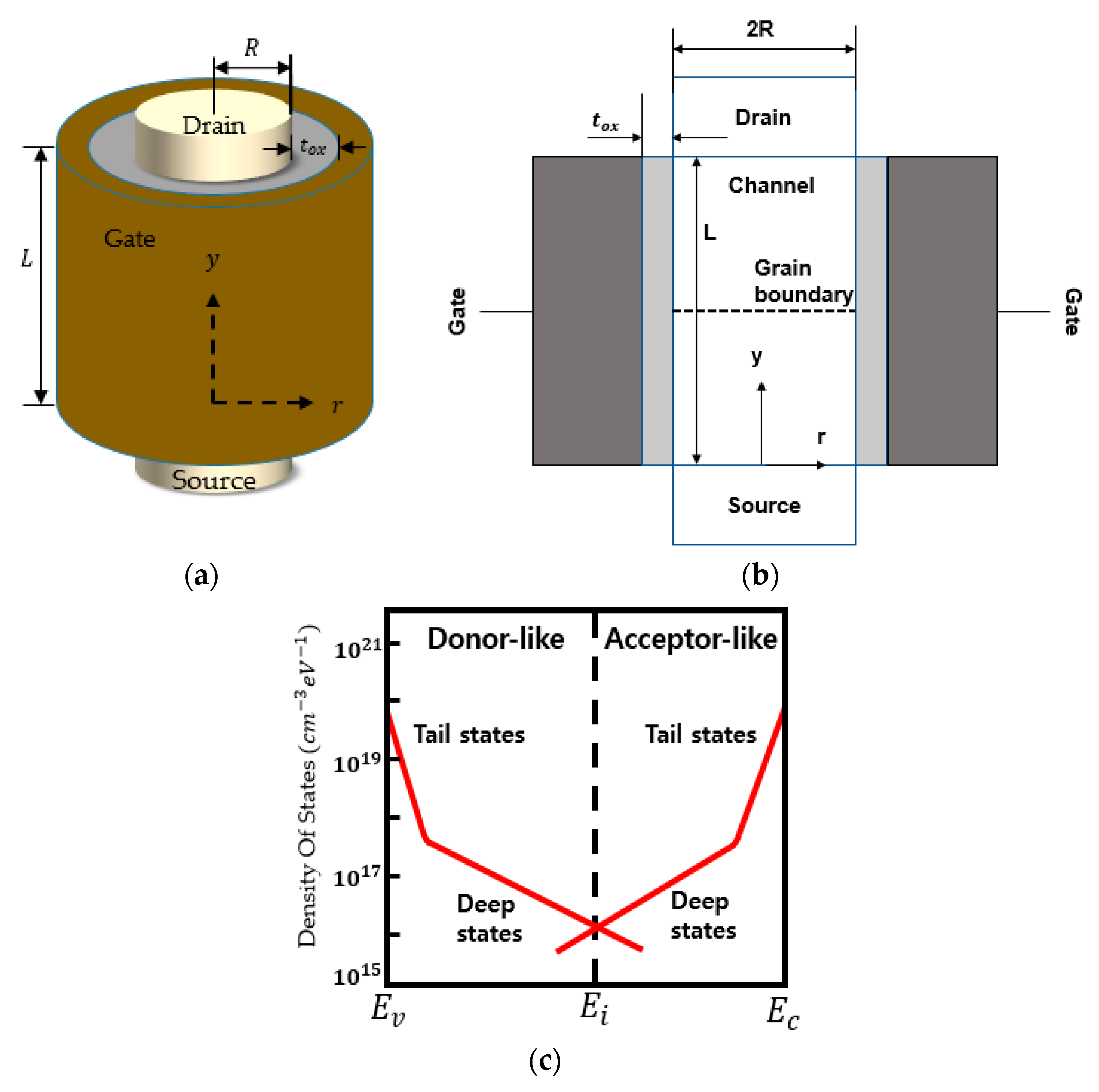
2. Analytical Drain Current Model for GAA Transistor with Poly-Crystalline Silicon Channel

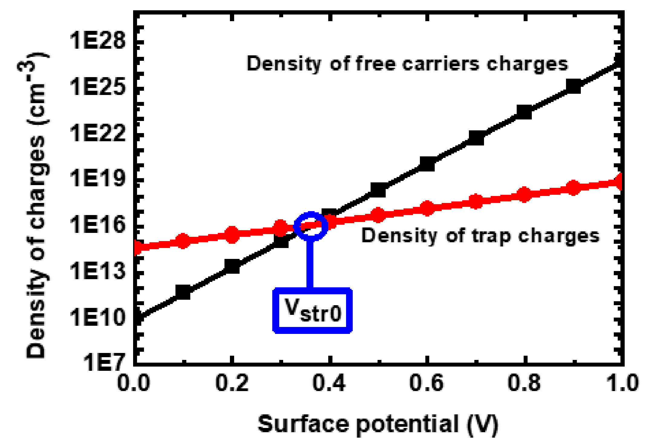
2.1. Electrostatic Potential Modeling

We considered a doped cylindrical GAA MOSFET, as shown in Figure 1. A highly doped drain and source regions ( 10 20   cm 3 ) have been assumed. Following the gradual channel approximation and considering the cylindrical coordinates, we can express the Poisson’s Equation as:
d 2 φ d r 2 + 1 r d φ d r = q ε s i [ n ( r ) + N T A + N a ]
where q is the electron charge, ε s i is the poly-silicon permittivity, n ( r ) is the free carrier charge density, which is expressed as n ( r ) = n i exp ( q ( φ V n ) / k T ) , N T A is the ionized acceptor like trap density, which is expressed as N T A = g c 1 [ π k T / sin ( π k T / E 1 ) ] exp ( E c / E 1 ) e x p ( q ( φ V n ) / E 1 ) and N a is the uniform doping concentration in the poly-silicon body. In this density Equation, n i is the intrinsic carrier concentration, V n is the channel potential, k is the Boltzmann constant, φ is the electrostatic potential, g c 1 is the density of states at the conduction band energy level, E 1   is the inverse slope of states, and E c is the conduction band energy level. In addition, the localized acceptor-like states, N TA , which are important for the n-channel device operation may be divided into two groups: ‘deep localized acceptor states’ and ‘tail states’ and E 1 is the characteristic energy slope of the density of localized acceptor states [13].
Equation (1) must satisfy three boundary conditions:
d φ d r ( r = 0 ) = 0
φ ( r = R ) = φ s
φ ( r = 0 ) = φ 0
where R is the radius of the channel so φ s is the surface potential and φ 0 is midpoint potential. To apply boundary conditions, Equation (1) should be rewritten using V s t r and V s u b , which determine dominant term in Equation (1). In strong inversion region, where V g s is larger than V s t r , the density of free carrier charges become dominant. We define V s t r as (Appendix A):
V s t r = V f b + V n + E 1 q · k T q · ln n i g c 1 π k T / sin π k T / E 1 exp E c / E 1 k T q E 1 q + q 4 ε s i R + t o x 2 R 2 · 2 n i exp E 1 q · ln n i g c 1 π k T / sin π k T / E 1 exp E c / E 1 k T q E 1 q + N a
where V f b is the flat band voltage and t o x is the oxide thickness. Hence Equation (1) can be rewritten as
d 2 φ d r 2 + 1 r d φ d r = q ε s i [ n i e x p ( q ( φ V n ) k T ) ]
When V g s is smaller than V s t r , we divide the subthreshold region by defining V s u b   , which becomes dominant between the trap density and the ionized acceptor concentration.
V s u b = V f b + V n + E 1 q · ln N a g c 1 π k T / sin π k T / E 1 exp E c / E 1 k T q E 1 q + q 4 ε s i R + t o x 2 R 2 · 2 N a + n i exp E 1 q · ln n i g c 1 π k T / sin π k T / E 1 exp E c / E 1 k T q E 1 q
When V g s < V s u b , the body doping charge term becomes dominant in Equation (1). We used the term n b in Equation (6) instead of N a . As a result, Equation (1) which considered only N a term can be expressed including electrostatic potential:
d 2 φ d r 2 + 1 r d φ d r = q ε s i [ n b e x p ( q ( φ V n ) V U _ b ) ]
where
a = ln 2 N a ln N a + g c 1 π k T / sin π k T / E 1 exp E c / E 1 e x p ( q · V n / E 1 V n + E 1 q ln q · N a E 1 b = ln N a + g c 1 π k T sin π k T / E 1 exp E c E 1 exp q · V n E 1 n b = e x p a V n + b V U _ b = 1 k
When V s t r > V g s > V s u b , the trap charge term becomes dominant in Equation (1):
d 2 φ d r 2 + 1 r d φ d r = q ε s i g c 1 π k T sin π k T / E 1 exp E c E 1 e x p q φ V n E 1
From Equations (4), (6) and (8), we get a unified Poisson’s Equation in the different operational regions as:
d 2 φ d r 2 + 1 r d φ d r = q ε s i [ n U e x p ( ( φ V n ) V U ) ]
where n U is n i ,   n b   and g c 1 [ π k T / sin ( π k T / E 1 ) ] exp ( E c / E 1 ) . V U is k T / q ,   V U _ b and E 1 / q respectively. To derive electrostatic potential, we use Debye length term and well-known mathematical solution ( z = A 2 ln ( B r 2 + 1 ) ,   where   A   and   B   are   constant ) . As a result, the electrostatic potential function can be expressed as [11,12]:
φ U ( r ) = V n 2 V U l n { R 2 L U β U [ 1 β U 2 r 2 R 2 ] }
where B = β U 2 / R 2 . Total mobile charge can be written as Q = C o x ( V g s V f b φ s ) , where C o x is the gate oxide capacitance, which is expressed as C o x = ε o x / ( R l n ( 1 + t o x / R ) ) . From Gauss’s law, the following relation is satisfied:
C o x ( V g s V f b φ s ) = Q = ε s i d φ d r | r = R
By substituting Equation (10) into Equation (11), the function about β U and V is derived:
( V g s V f b V ) 2 V U l n 2 L U R = l n β U ln ( 1 β U 2 ) + η β U 2 1 β U 2
where η = 2 ε s i / C o x R . We can rewrite Equation (12) as substituting β U 2 / 1 β U 2   as     K U . So, Equation (12) becomes following Equation (13):
( V g s V f b V ) 2 V U l n 2 L U R = ln ( K U ) 1 2 ln ( K U 1 + K U ) + η K U
By using Lambert W function [14], β U can be solved.
K U = W 0 { 2 η · e x p [ ( V g s V f b V ) 2 V U l n 2 L U R ] } 2 η + w ( y , y , y ) + ϵ
The first term in Equation (14) is the initial solution ( K U 0 ) . The second and third terms in Equation (14) are the correction term to improve the accuracy [15]. The second term w ( y , y , y ) is expressed as w ( y , y , y ) = ( y / y / ( 1 0.5 y y / y / y ) ) , where y = K U 0 2 + K U 0 exp { 2 [ ( V g s V f b V ) / 2 V U l n ( 2 L U / R ) η · K U 0 ] } . The third term can be calculated by ϵ = [ b + ( b 2 4 a c ) 1 2 ] / 2 a , where a = 1 2 η 2 e x p ( 2 [ ( V g s V f b V ) / 2 V U l n ( 2 L U / R ) η · K U 1 ] , b = 1 + 2 [ K U 1 + η e x p ( 2 [ ( V g s V f b V ) / 2 V U l n ( 2 L U / R ) η · K U 1 ] , c = K U 1 2 + K U 1 e x p { 2 [ ( V g s V f b V ) / 2 V U l n ( 2 L U / R ) η · K U 1 ] } and K U 1 = K U 0 + w ( y , y , y ) . As a result, β U can be solved from Equations (10) and (11) for a given V g s . We can then obtain the electrostatic potential by substituting β U into the RHS of Equation (10). To obtain the unified electrostatic potential, we use the smoothing function [9]:
φ s _ s u b = 1 m T ln [ 1 1 e x p ( m T φ s _ b o d y ) + 1 e x p ( m T φ s _ t r a p ) ]
φ s = 1 m T ln 1 1 e x p m T φ s _ f r e e + 1 e x p m T φ s _ s u b
where φ s _ s u b is the electric surface potential result considering the two terms, i.e., body doping and trap density in the subthreshold region. φ s _ b o d y and φ s _ t r a p are the surface potential dominated by the body uniform doping charge and trap charge, respectively. φ s _ f r e e is the surface potential dominated by the free carrier charges. m T is the weight parameter to connect the different asymptotical results.

2.2. Drain Current Modeling

We can obtain current Equation by using drift-diffusion current Equation I d s = μ e f f ( 2 π R ) Q d V / d y . Integrating this Equation from the source to the drain and changing from the function of V to the function of β , we can get the different expression of drift-diffusion current Equation (17):
I d s _ U = μ e f f 2 π R L 0 V d s Q i V d V = μ e f f 2 π R L β U _ S β U _ D Q i β U d V d β U d β U
where β U _ S and β U _ D are solved from Equation (13) corresponding to V = 0   and   V = V D S respectively.
Effective mobility can be defined to consider the grain boundary effect [16,17,18].
μ e f f = μ 0 [ exp ( θ 1 ( V d s   ) 1 θ 2 θ 3 ( V g s ) θ 4 ) ] 1 + θ 5 ( V g s ) θ 6 + θ 7 ( V g s ) θ 8 + θ 9 ( V d s ) θ 10
where μ 0 is the low-field mobility and θ 1 ~ θ 10 are the fitting parameters. We can obtain Q i ( β U ) = ε s i d φ s U / d r Q t Q b = ε s i 4 V U β U 2 / R ( 1 β U 2 ) Q t Q b from Equation (10) where Q t is trapped charge density, Q b is bulk charge density and d V / d β = 2 V U [ 1 / β U + 2 β U / 1 β U 2 + 2 η β U / ( 1 β U 2 ) 2 ] from Equation (12). By substituting this terms to Equation (17), we can get the drain current Equation (19):
I d s _ U = μ e f f ε s i 16 π L V U 2 · 1 2 ln 1 β U 2 + 1 η 1 β U 2 + η 2 1 β U 2 2 β U D β U S 2 μ e f f 2 π R L V U Q t + Q b [ ln β U 1 β U 2 + η 1 β U ] β U D β U S
Due to the difference in the current derivation method and approximation, there is a difference between the second term of Equation (19) and the current Equation in [11]. To calculate Q t , we should calculate   q g c 1 [ π k T / sin ( π k T / E 1 ) ] exp ( E c / E 1 ) exp ( q ( φ V n ) / E 1 ) r d r d θ / ( 2 π R ) . Instead of using this integral method, we use the trapezoid rule as:
Q t = q g c 1 π k T sin π k T / E 1 exp E c E 1 i = 1 n 1 { [ exp q φ i V n E 1 + exp q φ i + 1 V n E 1 h 2 } 2 R
To compute the drain current at the different operation region, we define three functions of f ( β ) , g ( β ) and h ( β ) :
f β = l n β U ln 1 β U 2 + η β U 2 1 β U 2
g ( β ) = [ 1 2 ln ( 1 β U 2 ) + 1 η 1 β U 2 + η 2 ( 1 β U 2 ) 2 ] | β U _ D β U _ S
h β = [ ln β U 1 β U 2 + η 1 β U ] β U D β U S
For a given V g s and V d s , β U _ S and β U _ D can be calculated from Equations (12) and (21a) f ( β U _ S ) = ( V g s V f b ) / 2 V U ln ( 2 L U / R ) and f ( β U _ D ) = ( V g s V f b V d s ) / 2 V U ln ( 2 L U / R ) . Following the approach of D. Jimenez [12], we can derive the analytical drain current Equation with closed-form by carefully checking the fluctuation of f ( β ) and β , which has different values at each operation region.
(1) Linear region above threshold
In this region, f ( β U _ S ) ,   f ( β U _ D ) 1 , thus β U _ S ,     β U _ D   ~   0 . Hence, the term η / 2 ( 1 β U _ S , D 2 ) 2 in g ( β U _ S , D ) becomes dominant and the term η / 1 β U _ S , D in h ( β U _ S , D ) becomes dominant. As a result, the drain current Equation is derived as:
I d s _ U = μ e f f W L C o x [ ( V g s V t 1 2 V d s ) V d s ] μ e f f W L ( Q t + Q b ) V d s
where V t = V 0 2 η V U and V 0 = V f b + 2 V U · l n ( 2 L U / R ) .
(2) Saturation region
In this region, f ( β U _ S ) 1 and f ( β U _ D ) 1 thus β U _ S   ~   0 and β U _ D   ~   1 . Hence, the term η / 2 ( 1 β U _ S 2 ) 2 in g ( β U _ S ) becomes dominant, the term ( 1 η ) / ( 1 β U _ D 2 ) + η / 2 ( 1 β U _ D 2 ) 2 in g ( β U _ D ) becomes dominant, the term η / 1 β U _ S in h ( β U _ S ) becomes dominant, and the term ln ( β U _ D / ( 1 β U _ D 2 ) ) + η / ( 1 β U _ D ) in h ( β U _ D ) becomes dominant. As a result, the drain current Equation is derived as:
I d s _ U = μ e f f W L C o x 2 [ ( V g s V t ) 2 V U 2 { 4 η 2 ( 1 exp ( V g s V 0 V d s V U ) ) 2 + 8 η ( 1 η ) 1 exp ( V g s V 0 V d s V U ) } ] μ e f f W L ( Q t + Q b ) [ ( 2 η V U + V d s ) 2 V U { η 1 exp ( V g s V 0 V d s V U ) ln ( 1 exp ( V g s V 0 V d s V U ) ) } ]
(3) Subthreshold region
In this region, f ( β U _ S ) ,   f ( β U _ D ) 1 , thus β U _ S , β U _ D   ~   1 . Hence, the term ( 1 η ) / ( 1 β U _ S , D 2 ) + η / 2 ( 1 β U _ S , D 2 ) 2 in g ( β U _ S , D ) becomes dominant and the term ln ( β U _ S , D / ( 1 β U _ S , D 2 ) ) + η / ( 1 β U _ S , D ) in h ( β U _ S , D ) becomes dominant. As a result, the drain current Equation is derived as:
I d s _ U = 2 μ e f f W L V U 2 ε s i R L U 2 exp V g s V f b V U 1 exp V d s V U 2 μ e f f W L V U Q t + Q b V d s 2 V U + η R 2 4 L U 2 exp V g s V f b V U 1 exp V d s V U
Finally, to get the unified electrostatic potential, we use smoothing function:
I d s _ s u b = 1 1 I d s _ b o d y m v + 1 I d s _ t r a p m v 1 m v
I d s = 1 1 I d s _ f r e e m v + 1 I d s _ s u b m v 1 m v
where I d s _ f r e e , I d s _ b o d y and I d s _ t r a p are the drain current dominated by free carriers charge, body doping charge and trap charge respectively. m v is weight parameter. As shown in the linear region, threshold voltage can be expressed as V t = V 0 2 η V U . If V t is written as a function of R, the following Equation (27) is obtained:
V t = V f b + 2 V U · l n 2 L U 2 V U l n R 1 + t o x R 2 ε s i ε o x

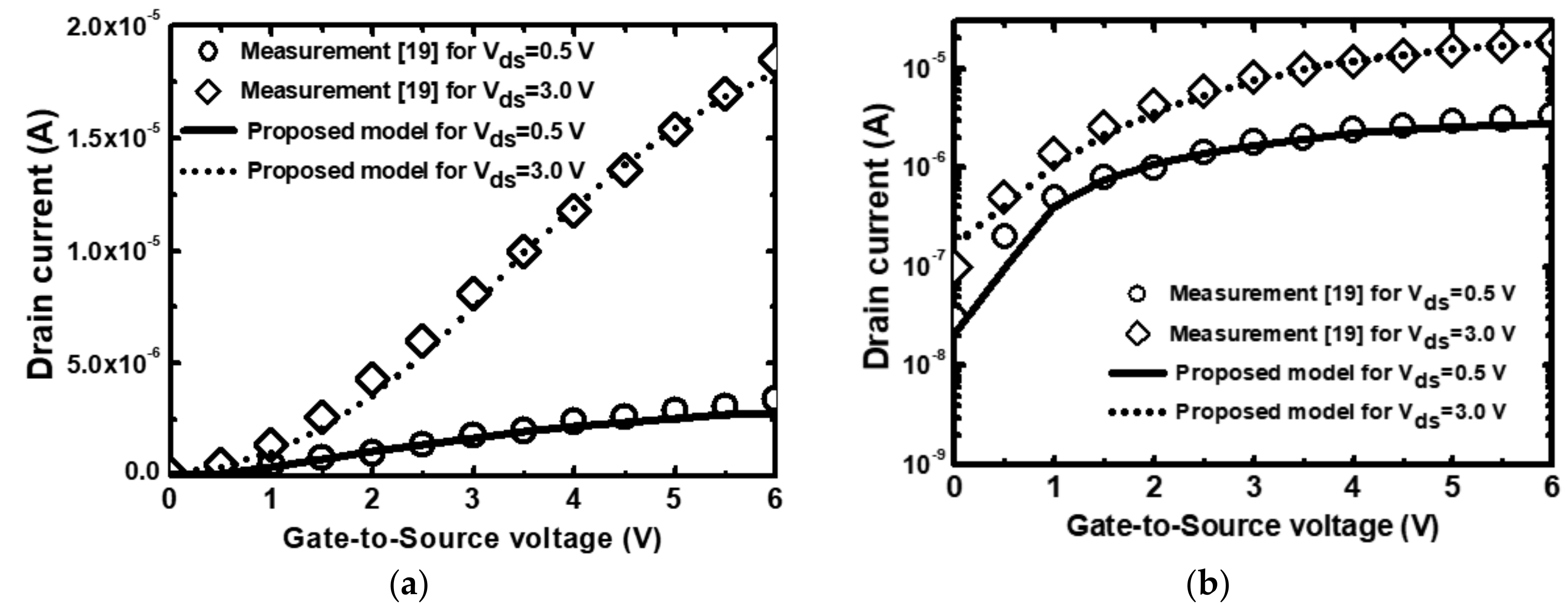
3. Results and Discussion

Figure 2a represents the electrostatic potential from boundary conditions (Equations (2b) and (2c)). From Equation (10), the surface potential is solved by substituting r to R. Likewise, the midpoint potential is solved by substituting r to zero. Figure 2 shows that in the subthreshold region, where the gate voltage is smaller than V s t r , the surface potential and midpoint potential are linear as the gate voltage increases. After the subthreshold region, each potential value is saturated in the strong inversion region. Figure 2b shows the surface potential at different channel potentials. The surface potential increases as V n increases.
The values of the parameters in Table 1 refer to the values extracted for the fabricated device through the actual process [11,19]. We divided the current Equation into three operation regions, as represented by Equations (22)–(24). Figure 3 shows the drain current versus drain-to-source voltage curve. This I-V curve can be drawn by using the current value of the linear region and the current value of the saturation region. As shown in Figure 3, we obtained the drain current value for different gate-to-source voltages. As the gate-to-source voltage increases, the saturation point increases and its current value increases. In addition, in this graph, we compared the GAA MOSFET devices with poly-silicon channel and the GAA MOSFET devices with single-crystalline silicon channel.
As shown in the Figure 3, devices using single-crystalline silicon channels show higher current values when compared to poly-silicon with grain boundary as expected. However, as the gate voltage increases, electrons are occupied at the trap. So the difference is smaller than when the gate voltage is low.
Figure 4 shows the graph where drain current is plotted against the gate-to-source voltage for low and high drain-to-source voltages. This I-V curve can be plotted by using the current value of the subthreshold voltage region and the current value of the linear region at low drain-to-source voltages. At high drain-to-source voltages, we used the current values of the subthreshold voltage region and the saturation region. As shown in Figure 4, the high drain-to-source voltage has a larger current value than the low drain-to-source voltage because of a lower barrier region.

4. Conclusions

In this work, we proposed an analytical current-voltage model of GAA transistor using poly-silicon channel. The proposed model considers both GAA cylindrical coordinates and poly-silicon grain boundary trap effects. It is a channel potential-based model that calculates the potential at the center of the substrate and the surface. Using the obtained channel potentials and the D. Jimenez approach, a useful and intuitive drain current-voltage and threshold voltage model Equation are derived by taking the appropriate approximation in each transistor's operating region (linear, saturation and sub-threshold regions). The proposed model shows high consistency when compared with the measured results which is the actual performance measured by applying NH 3 plasma treatment to reduce the trap-state density on poly-silicon TFT with GAA structure.

Author Contributions

Investigation, J.K.; Software, S.K.; Supervision, J.J.; Writing—original draft, Y.S.

Funding

This research was supported by the MOTIE (Ministry of Trade, Industry & Energy (10085645) and KSRC (Korea Semiconductor Research Consortium) support program for the development of the future semiconductor device, and partly by the National Research Foundation of Korea (NRF) grant funded by the Korea government(MSIT) (No. 2017R1C1B5077154).

Acknowledgments

The EDA tool was supported by the IC Design Education Center (IDEC), Korea.

Conflicts of Interest

The authors declare no conflict of interest.

Appendix A

Figure A1. The density of charges versus surface potential.
Electronics 08 00988 g0a1
As shown in Figure A1, at specific value, density of free carrier charges over density of trap charges. We defined this crossover point as V s t r 0 and we expressed it as function of voltage shown in the following method.
n i exp ( q ( V s t r 0 V n ) k T ) = g c 1 [ π k T sin ( π k T / E 1 ) ] exp ( E c E 1 ) e x p ( q ( V s t r 0 V n ) E 1 )
V s t r 0 can be defined by Equation (A1).
V s t r 0 = V n + E 1 q · k T q · ln ( n i g c 1 [ π k T / sin ( π k T / E 1 ) ] exp ( E c / E 1 ) ) k T q E 1 q  
At this point, density of free carrier charges and density of trap charges are same value. So rewrite the Poisson’s Equation (1).
d 2 φ d r 2 + 1 r d φ d r = q ε s i [ 2 n i exp ( q ( V s t r 0 V n ) k T ) + N a ]
Integrating the Equation (A3) results:
d φ d r = q r 2 ε s i [ 2 n i exp ( E 1 q · ln ( n i g c 1 [ π k T / sin ( π k T / E 1 ) ] exp ( E c / E 1 ) ) k T q E 1 q ) + N a ]  
From voltage relationship Equation,   V s t r can be written as V s t r = V s t r 0 + V f b + V o x and V o x can be calculated by:
V o x = R + t o x R d φ d r d r = q 4 ε s i [ 2 n i exp ( E 1 q · ln ( n i g c 1 [ π k T / sin ( π k T / E 1 ) ] exp ( E c / E 1 ) ) k T q E 1 q ) + N a ]       · [ ( R + t o x ) 2 R 2 ]
Hence, substitute Equations (A2) and (A5) into voltage relationship Equation (A6):
V s t r = V f b + V n + E 1 q · k T q · ln n i g c 1 π k T / sin π k T / E 1 exp E c / E 1 k T q E 1 q + q 4 ε s i R + t o x 2 R 2 · 2 n i exp E 1 q · ln n i g c 1 π k T / sin π k T / E 1 exp E c / E 1 k T q E 1 q + N a

References

  1. El Hamid, H.A.; Iñíguez, B.; Guitart, J.R. Analytical model of the threshold voltage and subthreshold swing of undoped cylindrical gate-all-around-based MOSFETs. IEEE Trans. Electron Devices 2007, 54, 572–579. [Google Scholar] [CrossRef]
  2. Chen, Y.; Luo, J. A comparative study of double-gate and surrounding gate MOSFETs in strong inversion and accumulation using an analytical model. Integration 2001, 1, 6. [Google Scholar]
  3. Fortunato, G. Polycrystalline silicon thin-film transistors: A continuous evolving technology. Thin Solid Film. 1997, 296, 82–90. [Google Scholar] [CrossRef]
  4. Nowak, E.; Kim, J.H.; Kwon, H.; Sim, J.S.; Lim, S.H.; Lee, K.H.; Park, Y.K.; Choi, J.H.; Chung, C. Intrinsic fluctuations in vertical NAND flash memories. In Proceedings of the 2012 Symposium on VLSI Technology (VLSIT), Honolulu, HI, USA, 12–14 June 2012; pp. 21–22. [Google Scholar]
  5. Yu, B.; Lu, H.; Liu, M.; Taur, Y. Explicit continuous models for double-gate and surrounding-gate MOSFETs. IEEE Trans. Electron Devices 2007, 54, 2715–2722. [Google Scholar]
  6. Yu, B.; Lu, W.Y.; Lu, H.; Taur, Y. Analytic charge model for surrounding-gate MOSFETs. IEEE Trans. Electron Devices 2007, 54, 492–496. [Google Scholar] [CrossRef]
  7. Lu, H.; Yu, B.; Taur, Y. A unified charge model for symmetric double-gate and surrounding-gate MOSFETs. Solid State Electron. 2008, 52, 67–72. [Google Scholar] [CrossRef]
  8. Li, X.; Deng, W.; Huang, J. A physical surface-potential-based drain current model for polysilicon thin-film transistors. J. Semicond. 2012, 33, 034005. [Google Scholar] [CrossRef]
  9. Deng, W.; Zheng, X.; Chen, R.; Liu, Y. Subthreshold characteristics of polysilicon TFTs. Solid State Electron. 2008, 52, 695–703. [Google Scholar] [CrossRef]
  10. Chen, S.S.; Shone, F.C.; Kuo, J.B. A closed-form inversion-type polysilicon thin-film transistor dc/ac model considering the kink effect. J. Appl. Phys. 1995, 77, 1776–1784. [Google Scholar] [CrossRef]
  11. Yu, F.; Deng, W.; Huang, J.; Ma, X.; Chen, S. An Explicit Physics-Based I-V Model for Surrounding-Gate Polysilicon Transistors. IEEE Trans. Electron Devices 2016, 63, 1059–1065. [Google Scholar] [CrossRef]
  12. Jiménez, D.; Iniguez, B.; Suñe, J.; Marsal, L.F.; Pallares, J.; Roig, J.; Flores, D. Continuous analytic IV model for surrounding-gate MOSFETs. IEEE Electron Device Lett. 2004, 25, 571–573. [Google Scholar] [CrossRef]
  13. Shur, M.; Hack, M. Physics of amorphous silicon based alloy field-effect transistors. J. Appl. Phys. 1984, 55, 3831–3842. [Google Scholar] [CrossRef]
  14. Corless, R.M.; Gonnet, G.H.; Hare, D.E.; Jeffrey, D.J.; Knuth, D.E. On the Lambert W function. Adv. Comput. Math. 1996, 5, 329–359. [Google Scholar] [CrossRef]
  15. Deng, W.; Huang, J. A physics-based approximation for the polysilicon thin-film transistor surface potential. IEEE Electron Device Lett. 2011, 32, 647–649. [Google Scholar] [CrossRef]
  16. Wang, M.; Wong, M.; Shi, X.; Zhang, D. Effective channel mobility of poly-silicon thin film transistors. In Proceedings of the 2006 8th International Conference on Solid-State and Integrated Circuit Technology Proceedings, Shanghai, China, 23–26 October 2006; pp. 1395–1397. [Google Scholar]
  17. Chern, H.N.; Lee, C.L.; Lei, T.F. An analytical model for the above-threshold characteristics of polysilicon thin-film transistors. IEEE Trans. Electron Devices 1995, 42, 1240–1246. [Google Scholar] [CrossRef]
  18. Xi, X. BSIM 4.5. 0 MOSFET Model User Manual. 2004; University of California: Berkeley, CA, USA, 2004. [Google Scholar]
  19. Sheu, J.T.; Huang, P.C.; Sheu, T.S.; Chen, C.C.; Chen, L.A. Characteristics of gate-all-around twin poly-Si nanowire thin-film transistors. IEEE Electron Device Lett. 2008, 30, 139–141. [Google Scholar] [CrossRef]
Figure 1. (a) 3-D scheme of the GAA MOSFETs with poly-silicon channel; (b) Cross-section of the GAA poly-silicon channel transistor; (c) Trap of exponential distribution in the poly-silicon channel.
Electronics 08 00988 g001
Figure 2. (a) Electrostatic surface potential and midpoint potential versus gate-to-source voltage at V n = 0 ; (b) Electrostatic surface potential at different value of V n
Electronics 08 00988 g002
Figure 3. Comparison of drain current versus drain-to-source voltage between proposed model, experimental results and single-crystalline silicon channel GAA MOSFETs.
Electronics 08 00988 g003
Figure 4. Comparison of drain current versus gate-to-source voltage between the proposed model and experimental results at low I d s _ U and high V d s ( 3.0   V ) voltages. (a) Linear scale; (b) Log scale.
Electronics 08 00988 g004
Table 1. Parameter Symbols and Values.
Symbol (units)ValueSymbol (units)Value
g c 1   ( c m 3 e V 1 ) 2 10 18 θ 3 0.002
N a   ( c m 3 ) 1 10 14 θ 4 2
E 1   ( e V ) 0.1 θ 5 0.01
L   ( μ m ) 2 θ 6 1
t o x   ( n m ) 27 θ 7 0.001
R   ( n m ) 35 θ 8 3
V f b   ( V ) 0 θ 9 0.01
μ 0   ( c m 2 V 1 s 1 ) 50 θ 10 1
θ 1 0.5 m T 20
θ 2 3 m v 10

