Article

Theoretical Study of InAlN/GaN High Electron Mobility Transistor (HEMT) with a Polarization-Graded AlGaN Back-Barrier Layer

1
School of Information Science and Technology, Nantong University, Nantong 226019, China
2
Department of Public Course Teaching, Shandong Polytechnic College, Jining 272067, China
3
School of Science, Jiangsu Provincial Research Center of Light Industrial Optoelectronic Engineering and Technology, Jiangnan University, Wuxi 214122, China
*
Author to whom correspondence should be addressed.
Electronics 2019, 8(8), 885; https://doi.org/10.3390/electronics8080885
Submission received: 18 July 2019 / Revised: 2 August 2019 / Accepted: 6 August 2019 / Published: 10 August 2019
(This article belongs to the Section Microelectronics)

Abstract

:
An inserted novel polarization-graded AlGaN back barrier structure is designed to enhance performances of In0.17Al0.83N/GaN high electron mobility transistor (HEMT), which is investigated by the two-dimensional drift-diffusion simulations. The results indicate that carrier confinement of the graded AlGaN back-barrier HEMT is significantly improved due to the conduction band discontinuity of about 0.46 eV at interface of GaN/AlGaN heterojunction. Meanwhile, the two-dimensional electron gas (2DEG) concentration of parasitic electron channel can be reduced by a gradient Al composition that leads to the complete lattice relaxation without piezoelectric polarization, which is compared with the conventional Al0.1Ga0.9N back-barrier HEMT. Furthermore, compared to the conventional back-barrier HEMT with a fixed Al-content, a higher transconductance, a higher current and a better radio-frequency performance can be created by a graded AlGaN back barrier.

1. Introduction

Over the years, gallium nitride (GaN) which is a typical representative of third-generation wide bandgap semiconductor materials, has attracted enormous interest due to it having a high critical electric field, electron gas owing to polarization, higher electron mobility and saturation velocity [1,2,3]. Therefore, the GaN-based high electron mobility transistors (HEMTs) allows us to achieve higher breakdown voltage, lower on-resistance and high operation switching frequency [4,5,6]. Considering the reliability problems of AlGaN/GaN HEMTs, which are caused by lattice defects due to lattice mismatch and piezoelectric effect at the AlGaN/GaN heterojunctions [7,8,9], an AlInN barrier layer has attractively replaced a commonly applied AlGaN barrier layer to improve performances of GaN-based HEMTs. The InxAl1−xN is lattice matched to GaN when the Al composition of InxAl1−xN is 0.83 [10]. Thus, a significantly higher two-dimensional electron gas (2DEG) density can be induced by spontaneous polarization at In0.17Al0.83N/GaN interface and the HEMT’s reliability can be enhanced [6,11,12,13,14]. An additional thin AlN interlayer is set between the AlInN barrier layer and the GaN channel layer to further improve performances of the In0.17Al0.83N/GaN HEMT. The AlN can increase discontinuity of the conduction band at heterojunction interface due to its larger forbidden band width, which plays a dominant factor for the significant increase of 2DEG concentration [15]. In addition, the AlN in In0.17Al0.83N/GaN heterojunction interface can reduce the alloy scattering which increases the mobility of the device [16]. Although the proposed InAlN/AlN/GaN structure has the stated advantages, part of the 2DEG will spill from the channel into the buffer layer, resulting in the reduction of mobility and reliability. It can be explained that GaN is both a buffer layer and a channel layer in a single heterojunction structure [17]. The most direct way to enhance the confinement of heterojunction 2DEG and suppress the overflow of carriers into the buffer layer is to use a back barrier, which constitutes a double heterojunction structure. Recently, many researches have reported on effects of the AlGaN back-barrier layers on the HEMTs with the double heterojunction structures [18,19,20,21]. To some extent, it can enhance carrier confinement but also produce an unwanted parasitic channel at the AlGaN back-barrier/GaN buffer interface. According to our previous works [22,23], the graded AlGaN back-barrier with Al content changing linearly from 0 to 0.1 can weaken the polarization between AlGaN and GaN buffer layer, and reduce the adverse effect of parasitic channel.
In this work, we propose a conventional In0.17Al0.83N/AlN/GaN structure with a 25 nm-thick Al0.1Ga0.9N back-barrier layer that can improve confinement of the channel, but a parasitic channel would be generated at the Al0.1Ga0.9N barrier/GaN buffer interface. Therefore, a polarization-graded AlGaN back barrier replaces the Al0.1Ga0.9N back barrier to reduce the harm of parasitic channel. The Al composition of graded AlGaN back-barrier layer near the side of GaN main channel is 0.1, and gradually reduces to 0 far away from the main channel. Numerical simulations can support the design of non-conventional devices in a short time, and a large amount of works on devices have been investigated by Atlas-Silvaco physical simulation [24,25,26,27,28,29]. The electron distributions and the conduction band profiles of HEMTs with an Al0.1Ga0.9N back-barrier and a graded back-barrier are calculated by Atlas-Silvaco physical simulator. The influences of two structures on performances of the HEMTs are compared theoretically. The results indicate that confinement of 2DEG can be effectively enhanced by a polarization-graded back barrier. In addition, the electron concentration in the parasitic channels can be weakened by the AlGaN back barrier layer with a gradient of polarization. It is beneficial for the improvement of transconductance, drain current, current gain cut-off frequency and power gain cut-off frequency, compared with the conventional Al0.1Ga0.9N back-barrier HEMT.

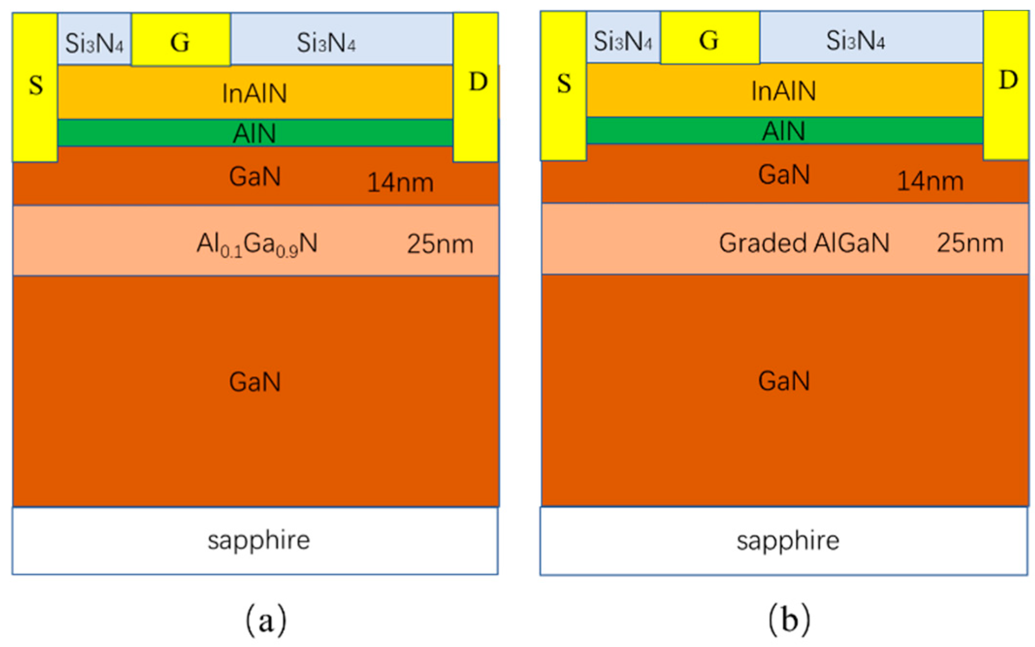
2. Device Description and Physical Models

Figure 1a,b shows the schematic cross-sectional diagram of the designed conventional HEMTs with an Al0.1Ga0.9N back barrier and a polarization-graded AlGaN back barrier. The epitaxial structure of an Al0.1Ga0.9N back-barrier HEMT was composed of a 2 μm unintentionally n-type doped GaN buffer layer, with a background carrier concentration of 1 × 1016cm−3 [30], a 1 nm AlN space layer, a 10 nm undoped In0.17Al0.83N barrier layer, a 14-nm-thick GaN channel and a 25 nm undoped Al0.1Ga0.9N back-barrier layer. Compared with the conventional back-barrier structure, the optimized structure introduced a 25 nm graded AlGaN back barrier with Al content linearly changing from 0% (bottom) to 10% (top) along the epitaxial growth. In both structures, Ohmic contacts were formed in the source and drain terminals. The distance of gate–source, gate–drain, and length of gate were 0.5 μm, 10 μm, and 2 μm, respectively. The device surface was passivated by using Si3N4 thin film to reduce the current collapse effect in the HEMT [31]. For all the simulations, donor trap was introduced at the In0.17Al0.83N with a trap level of 0.42 eV and a density of 3.86 × 1013cm−3 [32], while acceptor trap was considered in the unintentional doped (UID) GaN buffer with a trap level of 0.4 eV below the conduction band and a trap density of 1 × 1017 cm−3.
During the two-dimensional numerical calculation, the drift-diffusion transport model as well as several important physical models such as Fermi-Dirac, low field electron mobility, high field mobility, Shockley–Read–Hall (SRH) and polarization were used to simulate the device response. The physical parameters of GaN, AlN, Al0.1Ga0.9N and In0.17Al0.83N during the simulation are shown in Table 1 [33,34,35,36].
The two mobility models have been used to consider various types of scattering mechanisms [37]. The low field mobility model can be given by [34]:
1 u ( N , T ) = a ( N 1 × 10 17 ) ( T 300 ) 3 2 × l n [ 1 + 3 ( T 300 ) 2 ( N 1 × 10 17 ) 2 3 ] + b ( T 300 ) 3 2 + c exp ( 1065 T ) 1
where a = 2.61 × 10 4 / V s cm 2 , b = 9.8 × 10 4 / V cm 2 and c = 1.7 × 10 2 / V s cm 2 . u(N,T) is the mobility as a function of doping and ambient temperature, N is the total doping concentration, and T is the ambient temperature.
The high field mobility model can be specified as below [38]:
u ( E ) = u ( N , T ) + v s a t E ( N 1 1 ) E c N 1 1 + a n ( E E c ) N 2 + ( E E c ) N 1 ,
where u(N,T) is the low field mobility, υsat is saturation velocities, and E is the electric field. The values of Ec, an, N1, and N2 can be referred to [38].
SRH and Fermi–Dirac statistics are also considered. SRH recombination occurs when an electron gets trapped, referring to a trap-assisted recombination process. In order to investigate the specific physical mechanism of electron trapping, electron trapping process of each trap level should be calculated in the SRH recombination model. The rate of electron trapping [38,39,40,41] is given by
R n e t S R H = p n n i e 2 τ p [ n + n i e e x p ( E t r a p k T ) ] + τ n [ p + n i e e x p ( E t r a p k T ) ] ,
where Etrap is the difference between the trap energy level and intrinsic Fermi level, nie is intrinsic carrier concentration, and T is the lattice temperature. τn and τp are the lifetimes of electrons and holes, respectively, both of which are assumed to be 10−9 s.
Polarization modeling is critical for GaN based devices. Here, PPE and PSP represent the piezoelectric polarization and spontaneous polarization, respectively. The total polarization-induced polarization charge density is defined as [35]:
P t o t a l = [ P P E ( b o t t o m ) + P S P ( b o t t o m ) ] [ P P E ( t o p ) + P S P ( t o p ) ]
Since In0.17Al0.83N/GaN is lattice-matched and the graded back barrier layer is assumed as complete lattice relaxation, the sum of polarization in the device is spontaneous polarization without any piezoelectric polarization. A space polarization-induced charge would be generated by a gradient of polarization of the AlxGa1−xN back barrier which varies along the growth direction. The corresponding density is given by [42,43]:
ρ P = P = P Z .
With
P = P s p ( A l x G a 1 x N ) = x P s p ( A l N ) + ( 1 x ) P s p ( G a N ) .

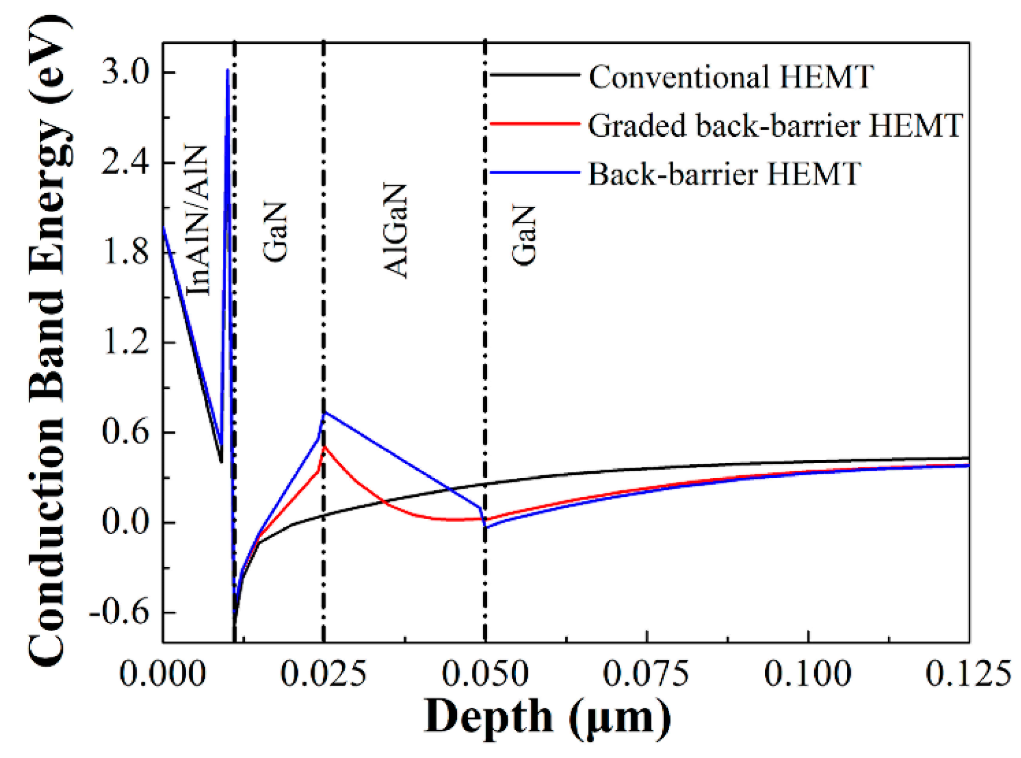
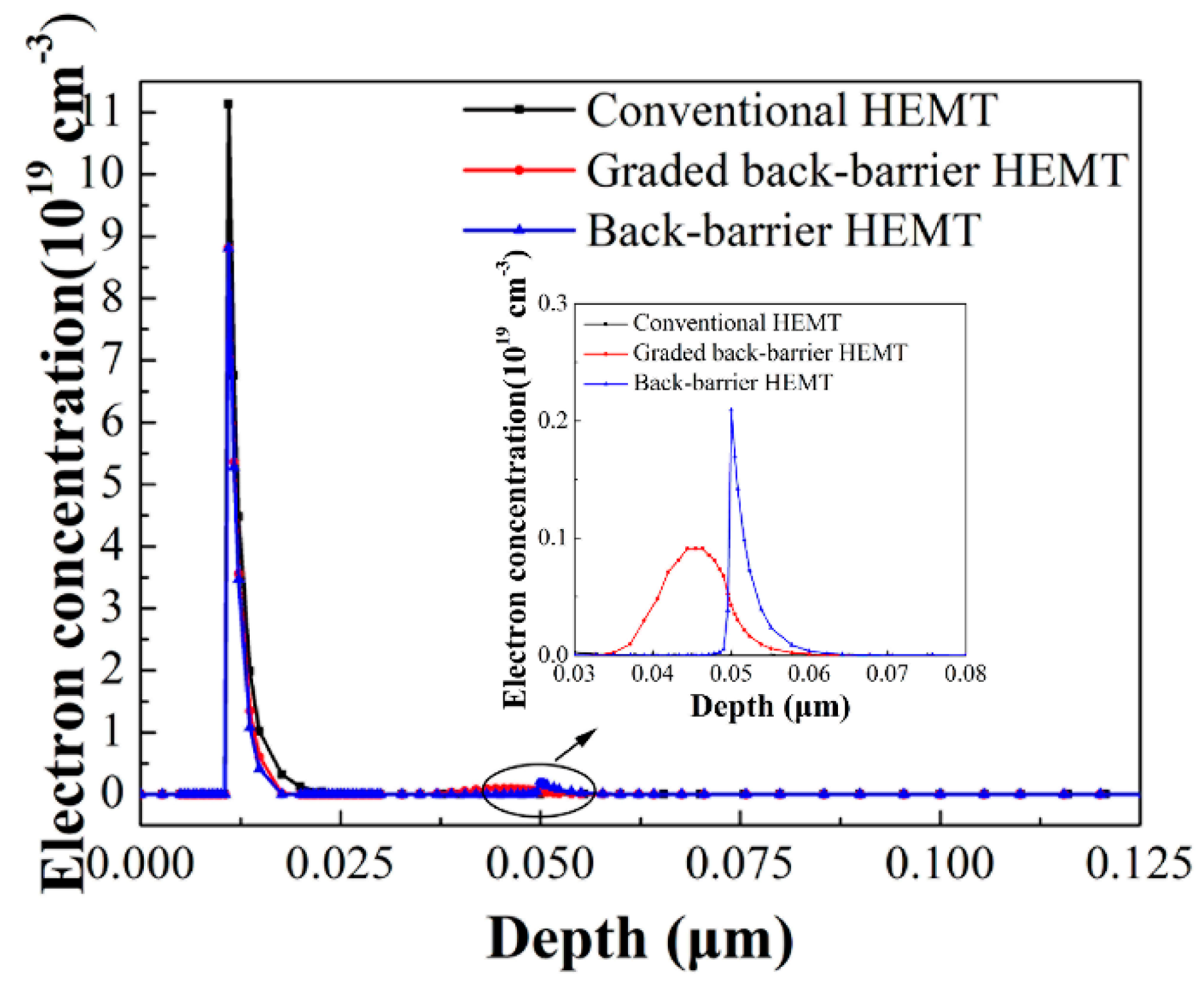
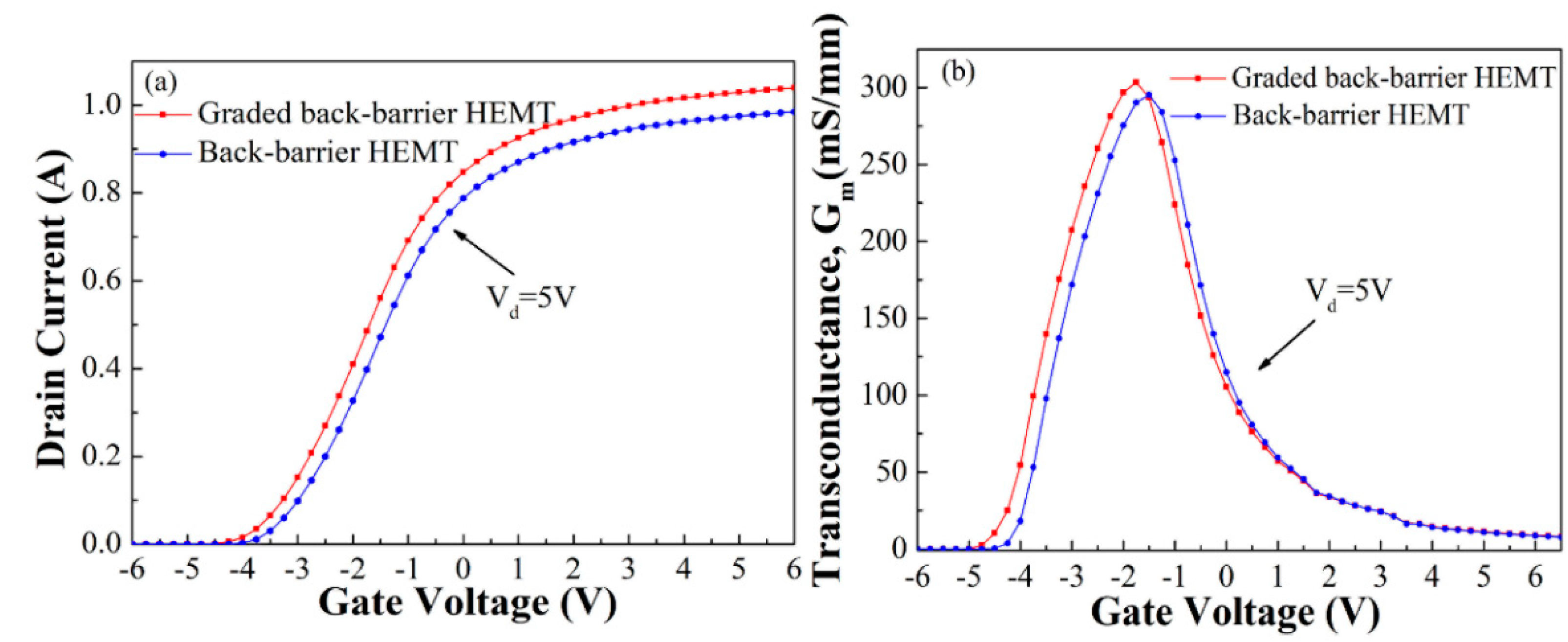
3. Results and Discussion

The conduction band diagrams of two different structures with back barrier under zero bias voltage calculated by two-dimensional self-consistent simulations are shown in Figure 2. The conduction band diagram of a conventional HEMT was simulated to observe the conduction band discontinuity caused by a back-barrier layer. It is obvious that the back barrier can raise the conduction band edge of the side of the potential well and enhance confinement of the heterojunction 2DEG. Comparing with the HEMT with a single heterojunction structure, the conduction band edge of the potential well of the device with an Al0.1Ga0.9N back barrier is increased by 0.69 eV, while the structure with an Al-graded back barrier is increased by 0.46 eV. Furthermore, the depth of electron potential well of the parasitic electron channel at interface of AlGaN/GaN in the polarization-graded AlGaN back-barrier HEMT is shallower than that of the device with an Al0.1Ga0.9N back barrier. The results are attributed to a gradient of polarization of AlGaN, which results in the complete lattice relaxation in the graded AlGaN back barrier without any piezoelectric polarization.
Figure 3 shows the carrier distributions of the three different structures, it is evident that at the AlN/GaN interface generates the primary quantum well. The electron concentration of the conventional HEMT, graded back-barrier HEMT and back-barrier HEMT were about 11 × 1019cm−3, 8.81 × 1019cm−3, and 8.8 × 1019cm−3, respectively. Moreover, a shallower secondary quantum well was also produced at the interface between the AlGaN layer and the GaN buffer layer, demonstrating the formation of a conductive parasitic channel. It is obvious from the inset of Figure 3 that the 2DEG concentration of secondary quantum well in the graded AlGaN back-barrier HEMT was about 0.1×1019cm-3, lower than that of the secondary quantum well in the AlGaN back-barrier HEMT with 2DEG concentration of 0.2 × 1019 cm−3. Compared to the HEMT with a single heterojunction, the electron distribution of the main channel was narrowed due to a back-barrier layer, while the carrier distribution of the structure with a fixed Al-composition back barrier layer was narrower than that of the structure with a graded Al-composition back-barrier layer. In other words, the structure with a graded Al-composition contributes to the improved confinement of 2DEG and the weakening of the generation of parasitic channels.
Figure 4 specifically illustrates the two-dimensional contour map of the electron distribution inside the two HEMTs with different structure. Figure 4a,b corresponds to the polarization-graded AlGaN back-barrier HEMT and the Al0.1Ga0.9N back-barrier HEMT, respectively. It can be seen that the electron concentration at the AlN/GaN interface was the highest, and formed a 2DEG potential well, which is consistent with the results shown in Figure 2 and Figure 3. Figure 4a,b shows that the enhanced 2DEG confinement was obtained by introducing a back-barrier layer due to the creation of an obvious conduction band discontinuity. The electron concentration at 25 nm (GaN/AlGaN) shown in Figure 4a is higher than that in Figure 4b, while that at the 50 nm (AlGaN/GaN) is lower than Figure 4b. This is because the gradual change of the Al composition in AlGaN back barrier weakened the polarization effect between AlGaN back-barrier layer and GaN buffer layer.
Figure 5 displays the transfer characteristics of the two different structures at Vds = 5 V. It was found that the maximum saturation current and transconductance of the graded back-barrier HEMT can be increased compared with that of the Al0.1Ga0.9N back-barrier HEMT. Figure 5a shows the curves of Vg-Id (the threshold voltages are about –4.5 V and –4 V) corresponding to the graded back-barrier HEMT and the Al0.1Ga0.9N back-barrier HEMT, respectively, which shifted negatively. The reason is that the back-barrier layer generates a negatively polarization field and then the 2DEG are confined in a narrower potential well. In addition, the threshold voltage negatively shifts about 0.5 V due to attenuation of the negatively polarization field in the polarization-graded AlGaN back barrier and weaker confinement of carriers in the main channel, compared with that of the Al0.1Ga0.9N back-barrier HEMT. The variations in Gm with Vg for two devices are depicted in Figure 5b. The structure with a graded back barrier shows the Gm peak value of 304 mS/mm at Vgs = −1.75 V, which is higher than that of the structure with an Al0.1Ga0.9N back-barrier (295 mS/mm at Vgs = −1.5 V), indicating that an improved control of drain current by the gate voltage was obtained in the polarization-graded one. The increase in the peak transconductance results from the fact that the gradual Al composition can weaken the effect of the parasitic channel on the main channel and increase the mobility of the 2DEG.
Figure 6 represents the current-voltage (Id-Vd) output characteristics at Vg from 0 V to –5 V for the two devices. The density of the maximum drain saturation current of 1.25 mA/mm was obtained at Vgs = 0 V in a graded back-barrier HEMT, which was about 13.6% higher than that of the Al0.1Ga0.9N back-barrier HEMT (1.1 mA/mm at Vgs = 0 V). The larger drain current in a graded back-barrier HEMT was mainly due to the lower threshold voltage shown in Figure 5a, while the concentrations of electron in the graded back-barrier HEMT and the conventional Al0.1Ga0.9N back-barrier HEMT were nearly the same.
Based on the small-signal AC simulation, the frequency characteristics of the devices are discussed. The variations in the fmax and fT regarding to the change of gate voltage for the two HEMTs are shown in Figure 7. It can be seen that the RF performance was improved by a gradual Al-composition in the AlGaN back barrier. The device with a graded back barrier achieved a peak value of current gain cutoff frequency of 5 GHz and a peak value of power gain cutoff frequency of 19 GHz, which were both higher than that of the conventional one. The reasons for this result are mainly due to the higher transconductance and the higher output resistance resulting from a graded polarization in the AlGaN back barrier.

4. Conclusions

In summary, a lattice-matched In0.17Al0.83N/AlN/GaN HEMT with a polarization-graded AlGaN back barrier is proposed by two-dimensional analysis of Atlas drift-diffusion simulations. The improved performance of the graded back-barrier HEMT is systematically demonstrated by comparing to the HEMT with an AlGaN back barrier. The electron confinement in the channel is enhanced effectively by introducing a back barrier, resulting in the improved performance of the device. In addition, a gradient of polarization in the back barrier can reduce the 2DEG concentration in the parasitic channel and weaken adverse effect of the channel, which is beneficial to improve the electronic performance of the device. As a result, a polarization-graded AlGaN back barrier can be an alternative to a fixed Al-content AlxGa1−xN back barrier design to obtain a high-performance InAlN/GaN HEMTs.

Author Contributions

Conception and design of study: Y.G., H.S.; acquisition of data: D.C., J.Z.; analysis and /or interpretation of data: G.Y., Z.D., Y.D.; drafting the manuscript: Y.G.; revising the manuscript: J.Z., G.Y.; approval of the version of the manuscript to be published: H.S.

Funding

This research was funded by the National Natural Science Foundation of China (Nos. 61804084, 11604124).

Acknowledgments

The authors would like to thank editors and anonymous reviewers for their special effort.

Conflicts of Interest

The authors declare no conflict of interest.

References

  1. Mishra, U.K.; Parikh, P.; Wu, Y.F. AlGaN/GaN HEMTs-an overview of device operation and applications. Proc. IEEE 2002, 90, 1022–1031. [Google Scholar] [CrossRef]
  2. Mishra, U.K.; Shen, L.; Kazior, T.E.; Wu, Y.F. GaN-based RF power devices and amplifiers. Proc. IEEE 2008, 96, 287–305. [Google Scholar] [CrossRef]
  3. Frayssinet, E.; Knap, W.; Lorenzini, P.; Grandjean, N.; Massies, J.; Skierbiszewski, C.; Suski, T. High electron mobility in AlGaN/GaN heterostructures grown on bulk GaN substrates. Appl. Phys. Lett. 2000, 77, 2551–2553. [Google Scholar] [CrossRef] [Green Version]
  4. Visalli, D.; Van Hove, M.; Derluyn, J.; Degroote, S.; Leys, M.; Cheng, K.; Germain, M.; Borghs, G. AlGaN/GaN/AlGaN double heterostructures on silicon substrates for high breakdown voltage field-effect transistors with low on-resistance. Jpn. J. Appl. Phys. 2009, 48, 04C101. [Google Scholar] [CrossRef]
  5. Kuzuhara, M.; Tokuda, H. Low-loss and high-voltage III-nitride transistors for power switching applications. IEEE Trans. Electron Devices 2015, 62, 405–413. [Google Scholar] [CrossRef]
  6. Kuzmik, J. Power electronics on InAlN/(In) GaN: Prospect for a record performance. IEEE Electron Devices Lett. 2001, 22, 510–512. [Google Scholar] [CrossRef]
  7. Feng, Z.H.; Zhou, Y.G.; Cai, S.J.; Lau, K.M. Enhanced thermal stability of the two-dimensional electron gas in GaN/AlGaN/GaN heterostructures by Si3N4 surface-passivation-induced strain solidification. Appl. Phys. Lett. 2004, 85, 5248–5250. [Google Scholar] [CrossRef]
  8. Joh, J.; Alamo, J.D. Impact of electrical degradation on trapping characteristics of GaN HEMTs. In Proceedings of the 2008 IEEE International Electron Devices Meeting, San Francisco, CA, USA, 15–17 December 2008. [Google Scholar]
  9. Lin, Z.; Kim, H.; Lee, J. Thermal stability of Schottky contacts on strained AlGaN/GaN heterostructures. Appl. Phys. Lett. 2004, 84, 1585–1587. [Google Scholar] [CrossRef] [Green Version]
  10. Neuburger, M.; Zimmermann, T.; Kohn, E.; Dadgar, A.; Schulze, F.; Günther, M.; Witte, H.; BlӒsing, J.; Krost, A.; daumiller, I.; et al. Unstrained InAlN/GaN HEMT structure. Int. J. High Speed Electron. Syst. 2004, 14, 785–790. [Google Scholar] [CrossRef]
  11. Ge, M.; Cai, Q.; Zhang, B.H.; Chen, D.J.; Hu, L.Q.; Xue, J.J.; Lu, H.; Zhang, R.; Zheng, Y.D. Effects of the trap level in the unintentionally doped GaN buffer layer on optimized p-GaN gate AlGaN/GaN HEMTs. Phys. Status Solidi A 2018, 215, 1700368. [Google Scholar] [CrossRef]
  12. Kuzmík, J.; Kostopoulos, A.; Konstantinidis, G.; Carlin, J.F.; Georgakilas, A.; Pogany, D. InAlN/GaN HEMTs: A first insight into technological optimization. IEEE Trans. Electron Devices 2006, 53, 422–426. [Google Scholar] [CrossRef]
  13. Kuzmík, J. InAlN/(In) GaN high electron mobility transistors: Some aspects of the quantum well heterostructure proposal. Semicond. Sci. Technol. 2002, 17, 540–544. [Google Scholar] [CrossRef]
  14. Medjdoub, F.; Carlin, J.F.; Gaquière, C.; Grandjean, N.; Kohn, E. Status of the emerging InAlN/GaN power HEMT technology. Open Electr. Electron. Eng. J. 2008, 2, 1–7. [Google Scholar] [CrossRef]
  15. Shrestha, N.M.; Li, Y.; Chang, E.Y. Simulation study on electrical characteristic of AlGaN/GaN high electron mobility transistors with AlN spacer layer. Jpn. J. Appl. Phys. 2014, 53, 04EF08. [Google Scholar] [CrossRef] [Green Version]
  16. Teke, A.; Gokden, S.; Tulek, R.; Leach, J.H.; Fan, Q.; Xie, J.; Ozgur, U.; Morkoc, H.; Lisesivdin, S.B.; Ozbay, E. The effect of AlN interlayer thicknesses on scattering processes in lattice-matched AlInN/GaN two-dimensional electron gas heterostructures. New J. Phys. 2009, 11, 063031. [Google Scholar] [CrossRef]
  17. Khan, M.A.; Kuznia, J.N.; Van Hove, J.M.; Pan, N.; Carter, J. Observation of a two-dimensional electron gas in low pressure metalorganic chemical vapor deposited GaN-AlxGa1−xN heterojunctions. Appl. Phys. Lett. 1992, 60, 3027–3029. [Google Scholar] [CrossRef]
  18. Imanaga, S.; Kawai, H. Novel AlN/GaN insulated gate heterostructure field effect transistor with modulation doping and one-dimensional simulation of charge control. J. Appl. Phys. 1997, 82, 5843–5858. [Google Scholar] [CrossRef]
  19. Chen, C.Q.; Zhang, J.P.; Adivarahan, V.; Koudymov, A.; Fatima, H.; Simin, G. AlGaN/GaN/AlGaN double heterostructure for high-power III-N field-effect transistors. Appl. Phys. Lett. 2003, 82, 4593. [Google Scholar] [CrossRef]
  20. Lee, D.S.; Gao, X.; Guo, S. InAlN/GaN HEMTs with AlGaN back barriers. IEEE Electron Devcies Lett. 2011, 32, 617–619. [Google Scholar] [CrossRef]
  21. Meng, F.; Zhang, J.; Zhou, H. Transport characteristics of AlGaN/GaN/AlGaN double heterostructures with high electron mobility. J. Appl. Phys. 2012, 112, 023707. [Google Scholar] [CrossRef]
  22. Yao, C.J.; Yang, G.F.; Li, Y.J.; Sun, R.; Zhang, Q.; Wang, J.; Gao, S.M. Investigation of N-face AlGaN ultraviolet light-emitting diodes with composition-varying AlGaN electron blocking layer. Opt. Quant. Electron. 2016, 48, 31. [Google Scholar] [CrossRef]
  23. Yao, C.J.; Ye, X.C.; Sun, R.; Yang, G.F.; Wang, J.; Lu, Y.N.; Yan, P.F.; Cao, J.T.; Gao, S.M. High-performance AlGaN-based solar-blind avalanche photodiodes with dual-periodic III–nitride distributed Bragg reflectors. Appl. Phys. Express 2017, 10, 034302. [Google Scholar] [CrossRef]
  24. Wang, H.; Jiang, L.L.; Wang, N.; Yu, H.Y.; Lin, X.P. A Charge Storage Based Enhancement Mode AlGaN/GaN High Electron Mobility Transistor. Mater. Sci. Forum 2018, 913, 870–875. [Google Scholar] [CrossRef]
  25. Della Corte, F.G.; Pezzimenti, F.; Bellone, S.; Nipoti, R. Numerical simulations of a 4H-SiC BMFET power transistor with normally-off characteristics. Mater. Sci. Forum 2011, 679–680, 621–624. [Google Scholar] [CrossRef]
  26. Anvarifard, M.K.; Orouji, A.A. Proper Electrostatic Modulation of Electric Field in a Reliable Nano-SOI With a Developed Channel. IEEE Trans. Electron Devices 2018, 65, 1653–1657. [Google Scholar] [CrossRef]
  27. Pezzimenti, F. Modeling of the steady state and switching characteristics of a normally-off 4H-SiC trench bipolar-mode FET. IEEE Trans. Electron Devices 2013, 60, 1404–1411. [Google Scholar] [CrossRef]
  28. Della Corte, F.G.; de Martino, G.; Pezzimenti, F.; Adinolfi, G.; Graditi, G. Numerical simulation study of a low breakdown voltage 4H-SiC MOSFET for photovoltaic module-level applications. IEEE Trans. Electron Devices 2018, 65, 3352–3360. [Google Scholar] [CrossRef]
  29. Wang, Y.; Li, Z.Y.; Hao, Y.; Luo, X.; Fang, J.P.; Ma, Y.C.; Yu, H.Y.; Cao, F. Evaluation by Simulation of AlGaN/GaN Schottky Barrier Diode (SBD) With Anode-Via Vertical Field Plate Structure. IEEE Trans. Electron Devices 2018, 65, 2552–2557. [Google Scholar] [CrossRef]
  30. Faramehr, S.; Kalna, K.; Igić, P. Modeling of 2DEG and 2DHG in i-GaN capped AlGaN/AlN/GaN HEMTs. In Proceedings of the International Conference on Microelectronics, Belgrade, Serbia, 12–14 May 2014; pp. 81–84. [Google Scholar]
  31. Ochiai, M.; Akita, M.; Ohno, Y.; Kishimoto, S.; Maezawa, K.; Mizutani, T. AlGaN/GaN heterostructure metal-insulator-semiconductor high-electron-mobility transistors with Si3N4 gate insulator. Jap. J. Appl. Phys. 2003, 42, 2278–2280. [Google Scholar] [CrossRef]
  32. Han, T.; Zhao, H.; Peng, X.; Li, Y. Control of short-channel effects in InAlN/GaN high-electron mobility transistors using graded AlGaN buffer. Superlattice Microst. 2018, 116, 207–214. [Google Scholar] [CrossRef]
  33. MorkoC, H.; Cingolani, R.; Gil, B. Polarization effects in nitride semiconductor device structures and performance of modulation doped field effect transistors. Solid-State Electron. 1999, 43, 1909–1927. [Google Scholar] [CrossRef]
  34. Ambacher, O.; Smart, J.; Shealy, J.R.; Weimann, N.G.; Chu, K.; Murphy, M.; Schaff, W.J.; Eastman, L.F.; Dimitrov, R.; Wittmer, L.; et al. Two-dimensional electron gases induced by spontaneous and piezoelectric polarization charges in N- and Ga-face AlGaN/GaN heterostructures. J. Appl. Phys. 1999, 87, 3222–3233. [Google Scholar] [CrossRef]
  35. Ambacher, O.; Majewski, J.; Miskys, C.; Link, A.; Hermann, M.; Eickhoff, M.; Stutzmann, M.; Bernardini, F.; Fiorentini, V.; Tilak, V.; et al. Pyroelectric properties of Al (In) GaN/GaN hetero-and quantum well structures. J. Phys. Condens. Matter 2002, 14, 3399–3434. [Google Scholar] [CrossRef]
  36. Pelá, R.R.; Caetano, C.; Ferreira, L.G.; Furthmüller, J.; Teles, L.K. Accurate band gaps of AlGaN, InGaN, and AlInN alloys calculations based on LDA-1/2 approach. Appl. Phys. Lett. 2011, 98, 151907. [Google Scholar] [CrossRef]
  37. Goswami, A.; Trew, R.J.; Bilbro, G.L. Physics of gate leakage current in N-polar InAlN/GaN heterojunction field effect transistors. J. Appl. Phys. 2014, 116, 164508. [Google Scholar] [CrossRef]
  38. SILVACO Int. ATLAS User’s Manual; Device Simulation Software: Santa Clara, CA, USA, 2016; Available online: https://www.silvaco.com (accessed on 1 February 2013).
  39. Hall, R.N. Electron-hole recombination in germanium. Phys. Rev. 1952, 87, 387. [Google Scholar] [CrossRef]
  40. Shockley, W. Statistics of the recombinations of holes and electrons. Phys. Rev. 1952, 87, 835–842. [Google Scholar] [CrossRef]
  41. Megherbi, M.L.; Pezzimenti, F.; Dehimi, L.; Saadoune, M.A.; Della Corte, F.G. Analysis of trapping effects on the forward current-voltage characteristics of al-implanted 4H-SiC p-i-n Diodes. IEEE Trans. Electron Devices 2018, 65, 3371–3378. [Google Scholar] [CrossRef]
  42. Inoue, T.; Nakayama, T.; Ando, Y.; Kosaki, M.; Miwa, H.; Hirata, K.; Uemura, T.; Miyamoto, H. Polarization engineering on buffer layer in GaN-based heterojunction FETs. IEEE Trans. Electron. Devices 2008, 55, 483–488. [Google Scholar] [CrossRef]
  43. Li, C.; Li, Z.; Peng, D.; Ni, J.; Pan, L.; Zhang, D. Improvement of breakdown and current collapse characteristics of GaN HEMT with a polarization-graded AlGaN buffer. Semicond. Sci. Technol. 2015, 30, 035007. [Google Scholar] [CrossRef]
Figure 1. Schematic diagram of the designed lattice-matched In0.17Al0.83N /GaN high electron mobility transistor (HEMT) structure (a) with an Al0.1Ga0.9N back barrier and (b) with a graded AlGaN back barrier.
Electronics 08 00885 g001
Figure 2. The conduction band diagrams of the In0.17Al0.83N/AlN/GaN HEMT, HEMTs with graded back-barrier layer and Al0.1Ga0.9N back-barrier layer under zero applied voltage.
Electronics 08 00885 g002
Figure 3. The electron concentration distributions of the In0.17Al0.83N/AlN/GaN HEMT, the graded back-barrier HEMT and the Al0.1Ga0.9N back-barrier HEMT. The inset shows the electron concentration in the parasitic channel at AlxGa1−xN/GaN interface.
Electronics 08 00885 g003
Figure 4. Structure chromaticity plots of the electron concentration distributions inside the two different HEMT structures with (a) a graded AlGaN back barrier and (b) an Al0.1Ga0.9N back barrier.
Electronics 08 00885 g004
Figure 5. Calculated (a) gate voltage–drain current (Vg-Id) and (b) gate voltage–transconductance (Vg-Gm) transfer characteristics at drain voltage of 5 V for the HEMTs with a grade back barrier and an AlGaN back barrier.
Electronics 08 00885 g005
Figure 6. The drain voltage–drain current (Vd-Id) output characteristics at gate voltage from 0 V to –5 V for the two HEMT structures with (a) a graded AlGaN back barrier and (b) an Al0.1Ga0.9N back barrier.
Electronics 08 00885 g006
Figure 7. Simulated radio-frequency (RF) performance of the two devices at 8 V drain voltage.
Electronics 08 00885 g007
Table 1. Parameters of GaN, AlN, Al0.83In0.17N, Al0.1Ga0.9N in the simulation.
ParameterGaNAlNAl0.83In0.17NAl0.1Ga0.9N
Band gap (eV)3.426.154.623.58
Permittivity10.2810.3111.0410.28
Hole mobility (cm2/Vs)221482-
Saturated velocities (υsat) for electrons (107 cm/s)2.02.171.1-
Spontaneous polarization, Psp (C/m2)−0.034−0.090−0.072−0.038

