Design of a Novel Double Negative Metamaterial Absorber Atom for Ku and K Band Applications

 ,
,  ,
,  ,
,
Abstract
:1. Introduction
2. Design Methodology
3. Results
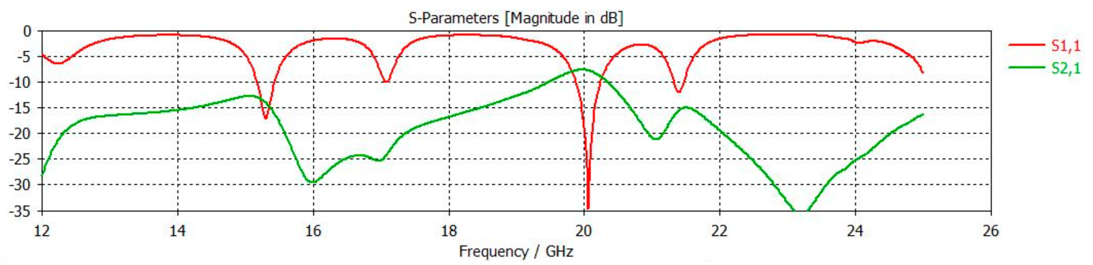
4. Discussion
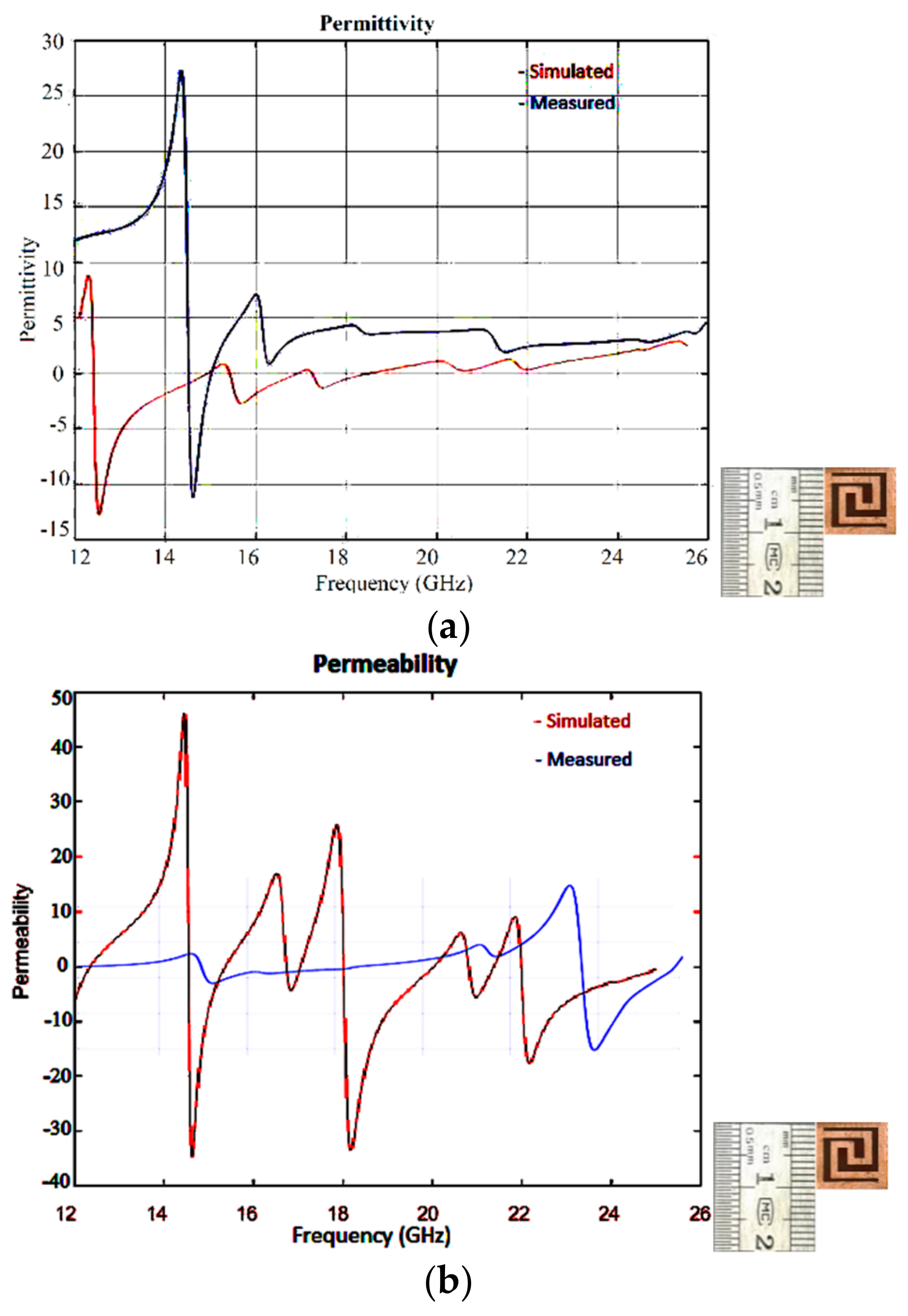
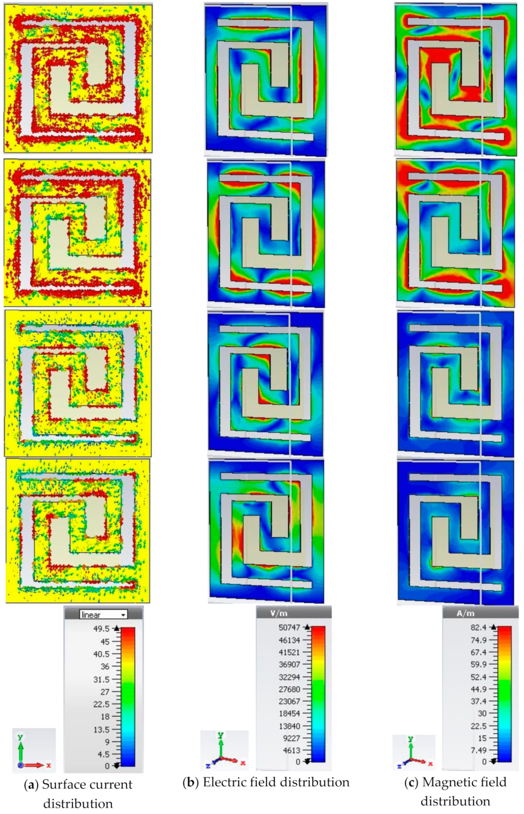
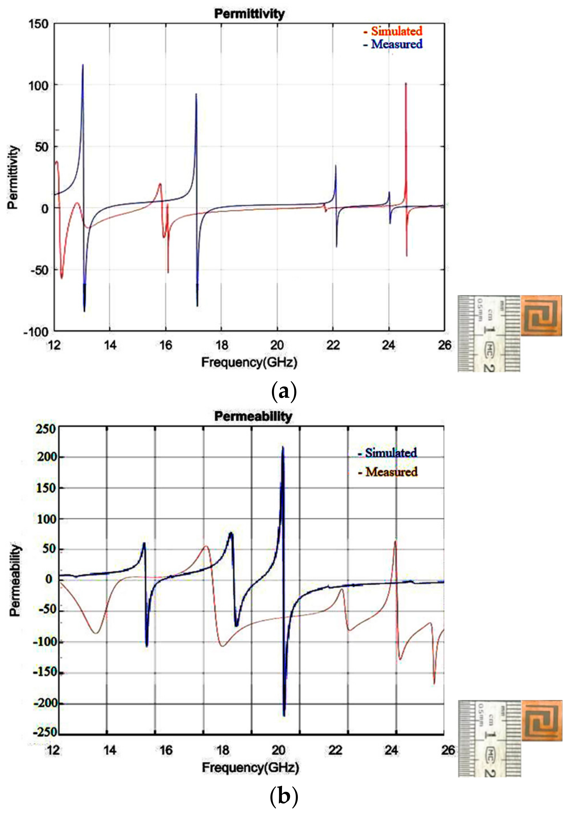
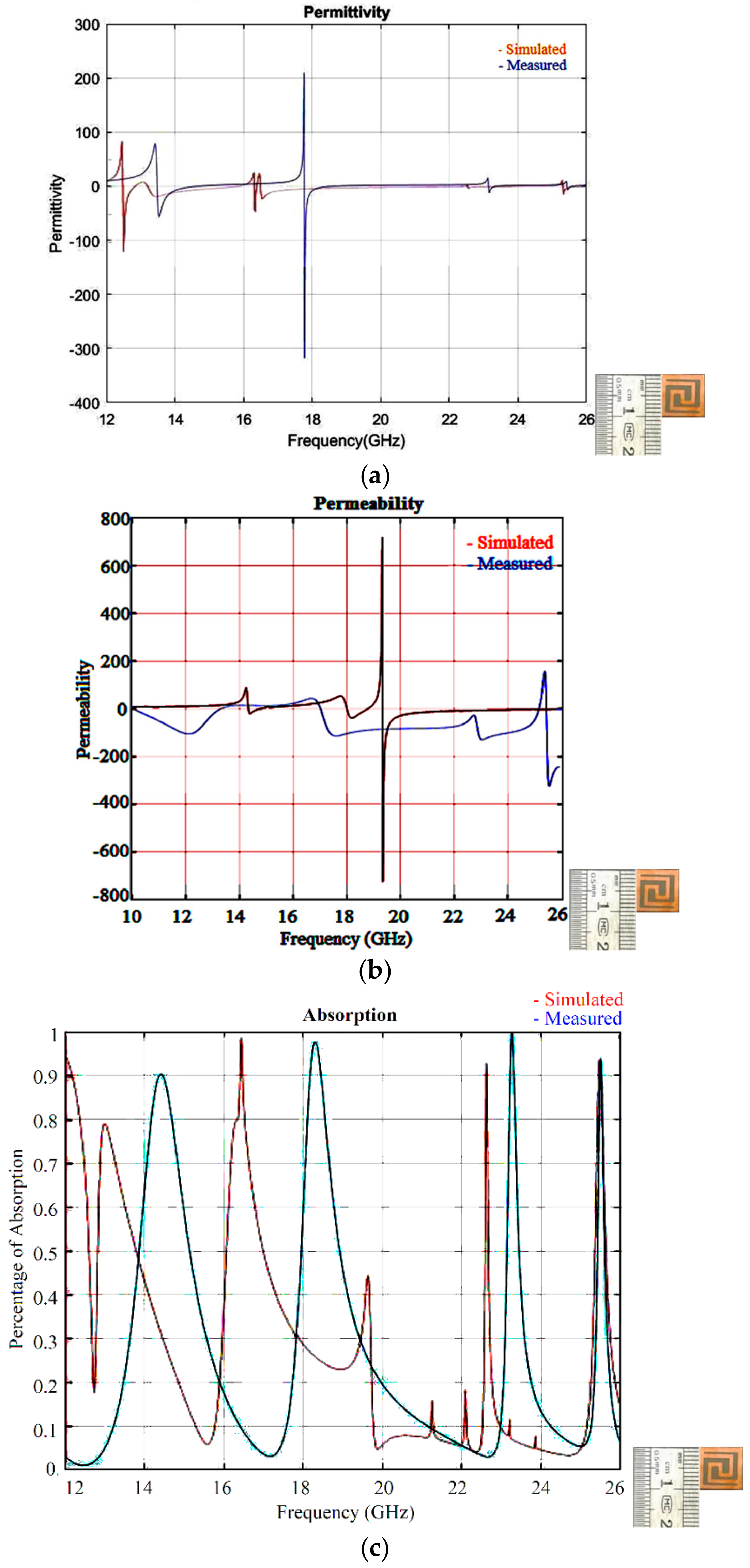
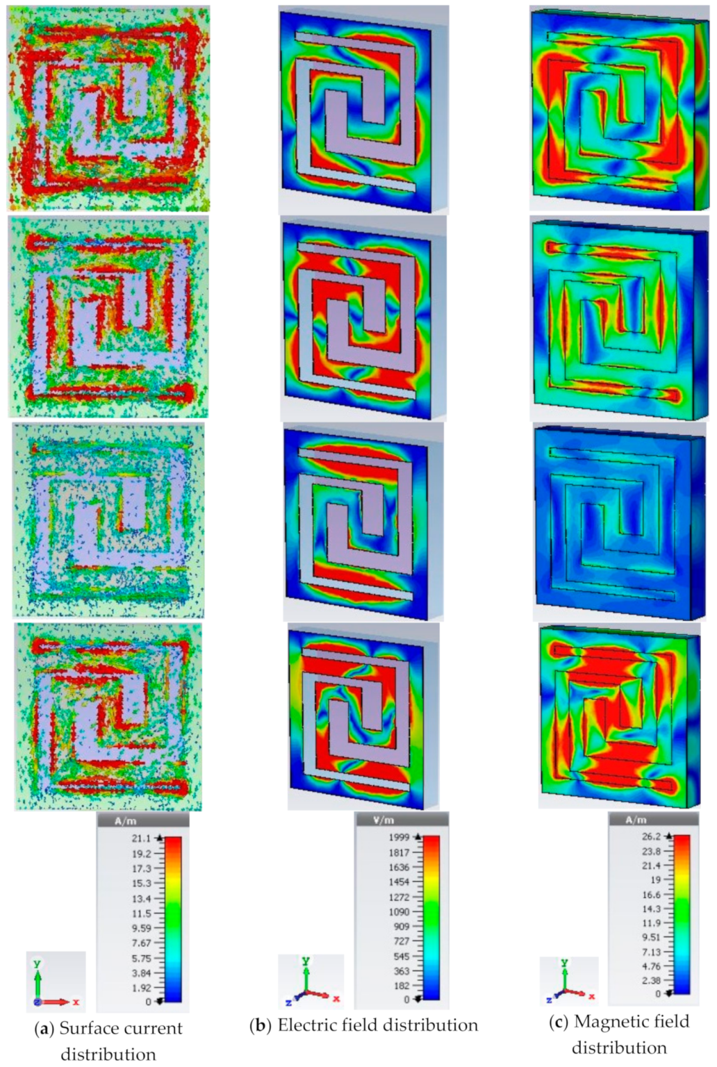
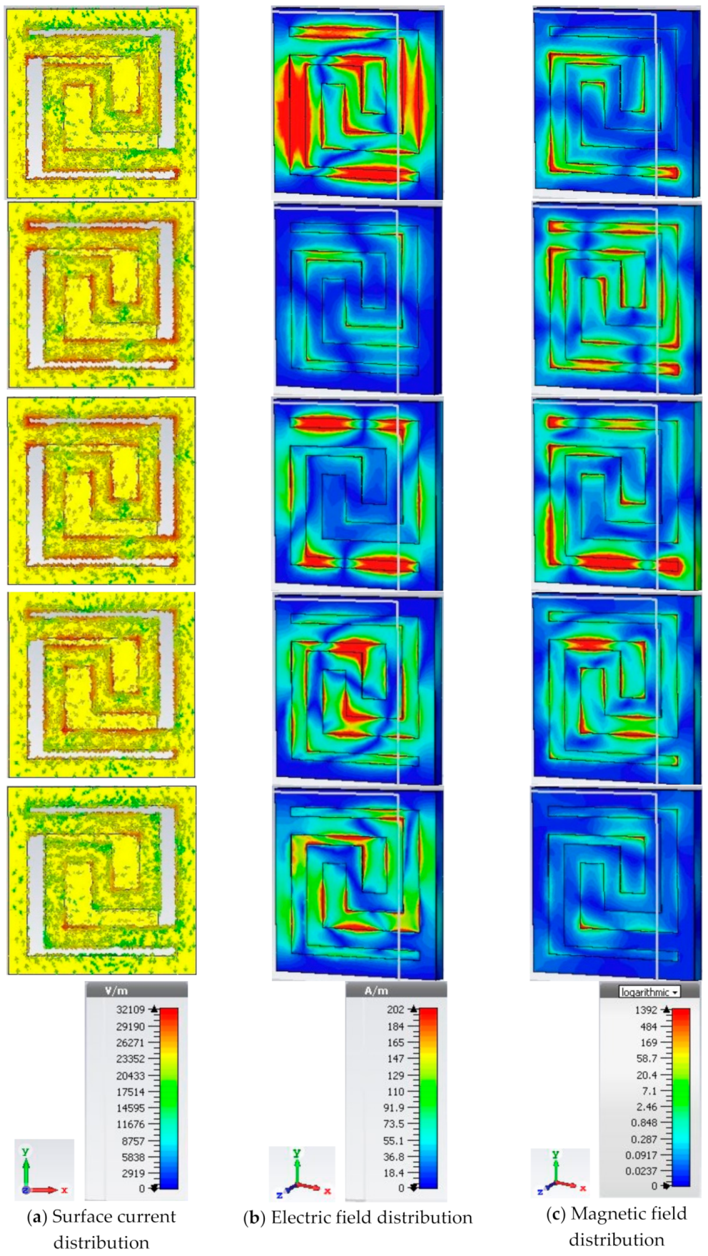
4.1. E-Field, H-Field and Surface Current Analysis
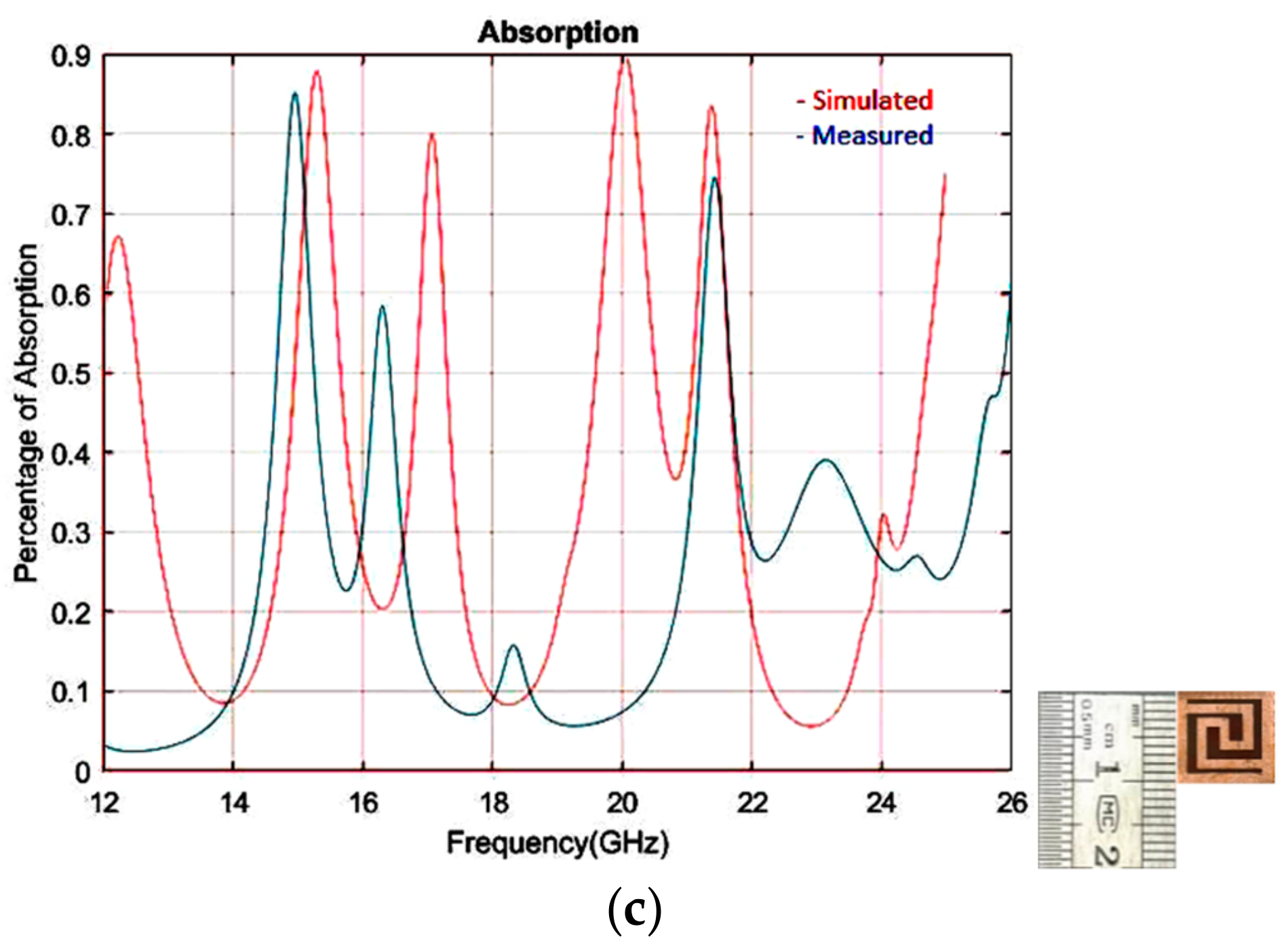
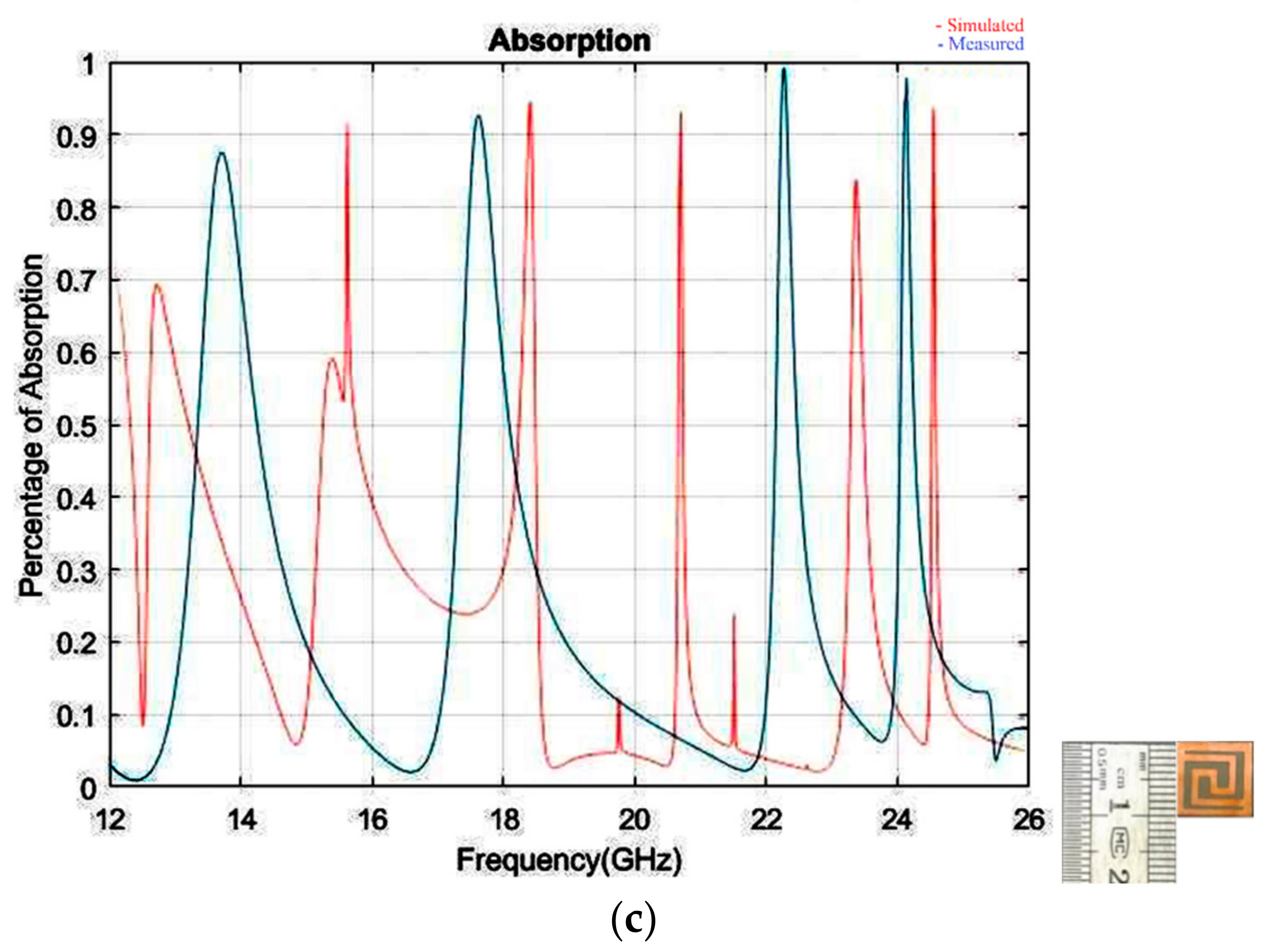
4.2. Absorption Performance Analysis
4.3. Comparison of the Unit Cell with Published Works
5. Conclusions
Author Contributions
Funding
Conflicts of Interest
References
- Sharma, A.; Panwar, R.; Khanna, R. Experimental Validation of a Frequency-Selective-Surface-Loaded Hybrid Metamaterial Absorber with Wide Bandwidth. IEEE Magn. Lett. 2019, 10, 1–5. [Google Scholar] [CrossRef]
- Xin, W.; Binzhen, Z.; Wanjun, W.; Junlin, W.; Junping, D. Design, fabrication, and characterization of a flexible dual-band metamaterial absorber. IEEE Photonics J. 2017, 9, 1–12. [Google Scholar] [CrossRef]
- Ghosh, S.; Lim, S. Perforated Lightweight Broadband Metamaterial Absorber Based on 3-D Printed Honeycomb. IEEE Antennas Wirel. Propag. Lett. 2018, 17, 2379–2383. [Google Scholar] [CrossRef]
- Mishra, N.; Choudhary, D.K.; Chowdhury, R.; Kumari, K.; Chaudhary, R.K. An investigation on compact ultra-thin triple band polarization independent metamaterial absorber for microwave frequency applications. IEEE Access 2017, 5, 4370–4376. [Google Scholar] [CrossRef]
- Zhou, Q.; Yin, X.; Ye, F.; Mo, R.; Tang, Z.; Fan, X.; Cheng, L.; Zhang, L. Optically transparent and flexible broadband microwave metamaterial absorber with sandwich structure. Appl. Phys. A 2019, 125, 131. [Google Scholar] [CrossRef]
- Abbasi, S.; Nourinia, J.; Ghobadi, C.; Karamirad, M.; Mohammadi, B. A sub-wavelength polarization sensitive band-stop FSS with wide angular response for X-and Ku-Bands. AEU Int. J. Electron. Commun. 2018, 89, 85–91. [Google Scholar] [CrossRef]
- Alam, M.J.; Faruque, M.R.I.; Azim, R.; Islam, M.T. Depiction and analysis of a modified H-shaped double-negative meta atom for satellite communication. Int. J. Microw. Wirel. Technol. 2018, 10, 1155–1165. [Google Scholar] [CrossRef]
- Veysi, M.; Kamyab, M.; Moghaddasi, J.; Jafargholi, A. Transmission phase characterizations of metamaterial covers for antenna application. Prog. Electromagn. Res. 2011, 21, 49–57. [Google Scholar] [CrossRef]
- Ullah, M.; Islam, M.; Faruque, M. A near-zero refractive index meta-surface structure for antenna performance improvement. Materials 2013, 6, 5058–5068. [Google Scholar] [CrossRef]
- Islam, M.; Islam, M.T.; Samsuzzaman, M.; Faruque, M.R.I. Compact metamaterial antenna for UWB applications. Electron. Lett. 2015, 51, 1222–1224. [Google Scholar] [CrossRef]
- Hasan, M.; Faruque, M.; Islam, S.; Islam, M. A new compact double-negative miniaturized metamaterial for wideband operation. Materials 2016, 9, 830. [Google Scholar] [CrossRef] [PubMed]
- Hoque, A.; Tariqul Islam, M.; Almutairi, A.; Alam, T.; Jit Singh, M.; Amin, N. A Polarization Independent Quasi-TEM Metamaterial Absorber for X and Ku Band Sensing Applications. Sensors 2018, 18, 4209. [Google Scholar] [CrossRef] [PubMed]
- Landy, N.I.; Sajuyigbe, S.; Mock, J.J.; Smith, D.R.; Padilla, W.J. Perfect metamaterial absorber. Phys. Rev. Lett. 2008, 100, 207402. [Google Scholar] [CrossRef] [PubMed]
- Kollatou, T.; Dimitriadis, A.; Assimonis, S.; Kantartzis, N.; Antonopoulos, C. Multi-band, highly absorbing, microwave metamaterial structures. Appl. Phys. A 2014, 115, 555–561. [Google Scholar] [CrossRef]
- Arjunan, A. Targeted sound attenuation capacity of 3D printed noise cancelling waveguides. Appl. Acoust. 2019, 151, 30–44. [Google Scholar] [CrossRef]
- Arjunan, A. Acoustic absorption of passive destructive interference cavities. Mater. Today Commun. 2019, 19, 68–75. [Google Scholar] [CrossRef]
- Li, H.; Yuan, L.H.; Zhou, B.; Shen, X.P.; Cheng, Q.; Cui, T.J. Ultrathin multiband gigahertz metamaterial absorbers. J. Appl. Phys. 2011, 110, 014909. [Google Scholar] [CrossRef]
- Kollatou, T.M.; Dimitriadis, A.I.; Assimonis, S.; Kantartzis, N.V.; Antonopoulos, C.S. A family of ultra-thin, polarization-insensitive, multi-band, highly absorbing metamaterial structures. Prog. Electromagn. Res. 2013, 136, 579–594. [Google Scholar] [CrossRef]
- Chen, H.; Yang, X.; Wu, S.; Zhang, D.; Xiao, H.; Huang, K.; Zhu, Z.; Yuan, J. Flexible and conformable broadband metamaterial absorber with wide-angle and polarization stability for radar application. Mater. Res. Express 2018, 5, 015804. [Google Scholar] [CrossRef]
- Chen, K.; Luo, X.; Ding, G.; Zhao, J.; Feng, Y.; Jiang, T. Broadband microwave metamaterial absorber with lumped resistor loading. EPJ Appl. Metamater. 2019, 6, 1. [Google Scholar] [CrossRef]
- Li, Y.; Wang, J.; Yang, J.; Wang, J.; Feng, M.; Li, Y.; Zhang, J.; Qu, S. Metamaterial anti-reflection lining for enhancing transmission of high-permittivity plate. J. Phys. D Appl. Phys. 2018, 52, 03LT01. [Google Scholar] [CrossRef]
- Zhi, Y.; Wang, Y.; Nie, Y.; Zhou, R.; Xiong, X.; Wang, X. Design, fabrication and measurement of a broadband polarization-insensitive metamaterial absorber based on lumped elements. J. Appl. Phys. 2012, 111, 044902. [Google Scholar]
- Singh, D.; Srivastava, V.M. Design Implementation of Concentric Loops with Stubs Metamaterial Absorber. Wirel. Pers. Commun. 2019, 104, 129–148. [Google Scholar] [CrossRef]
- Bilotti, F.; Toscano, A.; Alici, K.B.; Ozbay, E.; Vegni, L. Design of miniaturized narrowband absorbers based on resonant-magnetic inclusions. IEEE Trans. Electromagn. Compat. 2010, 53, 63–72. [Google Scholar] [CrossRef]
- Xin, W.; Binzhen, Z.; Wanjun, W.; Junlin, W.; Junping, D. Design and characterization of an ultrabroadband metamaterial microwave absorber. IEEE Photonics J. 2017, 9, 1–13. [Google Scholar] [CrossRef]
- Sen, G.; Islam, S.N.; Banerjee, A.; Das, S. Broadband perfect metamaterial absorber on thin substrate for X-band and Ku-band applications. Prog. Electromagn. Res. 2017, 73, 9–16. [Google Scholar] [CrossRef]
- Kumar, R.; Tripathy, M.R.; Ronnow, D. An Approach to Improve Gain and Bandwidth in Bowtie Antenna Using Frequency Selective Surface. In Smart Innovations in Communication and Computational Sciences; Springer: Berlin/Heidelberg, Germany, 2019; pp. 219–227. [Google Scholar]
- Lee, J.; Lim, S. Bandwidth-enhanced and polarisation-insensitive metamaterial absorber using double resonance. Electron. Lett. 2011, 47, 8–9. [Google Scholar] [CrossRef]
- Sim, M.S.; You, K.Y.; Esa, F.B.; Chan, Y.L. Broadband metamaterial microwave absorber for X-Ku band using planar split ring-slot structures. In Proceedings of the 2017 Progress in Electromagnetics Research Symposium-Fall (PIERS-FALL), Singapore, 19–22 November 2017; pp. 215–221. [Google Scholar]
- Madhav, B.; Krishna, T.R.; Lekha, K.D.S.; Bhavya, D.; Teja, V.D.; Reddy, T.M.; Anilkumar, T. Multiband Semicircular Planar Monopole Antenna with Spiral Artificial Magnetic Conductor. In Microelectronics, Electromagnetics and Telecommunications; Springer: Berlin/Heidelberg, Germany, 2018; pp. 599–607. [Google Scholar]
- Khan, S.; Eibert, T.F. A Multifunctional Metamaterial-Based Dual-Band Isotropic Frequency-Selective Surface. IEEE Trans. Antennas Propag. 2018, 66, 4042–4051. [Google Scholar] [CrossRef]
- Agrawal, A.; Misra, M.; Singh, A. Wide incidence angle and polarization insensitive dual broad-band metamaterial absorber based on concentric split and continuous rings resonator structure. Mater. Res. Express 2018, 5, 115801. [Google Scholar] [CrossRef]
- Jafari, F.S.; Naderi, M.; Hatami, A.; Zarrabi, F.B. Microwave Jerusalem cross absorber by metamaterial split ring resonator load to obtain polarization independence with triple band application. AEU Int. J. Electron. Commun. 2019, 101, 138–144. [Google Scholar] [CrossRef]


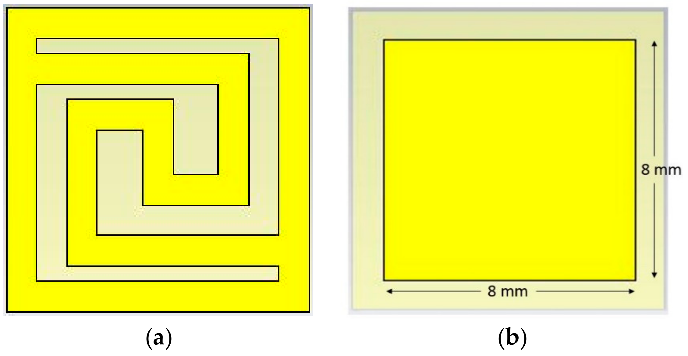
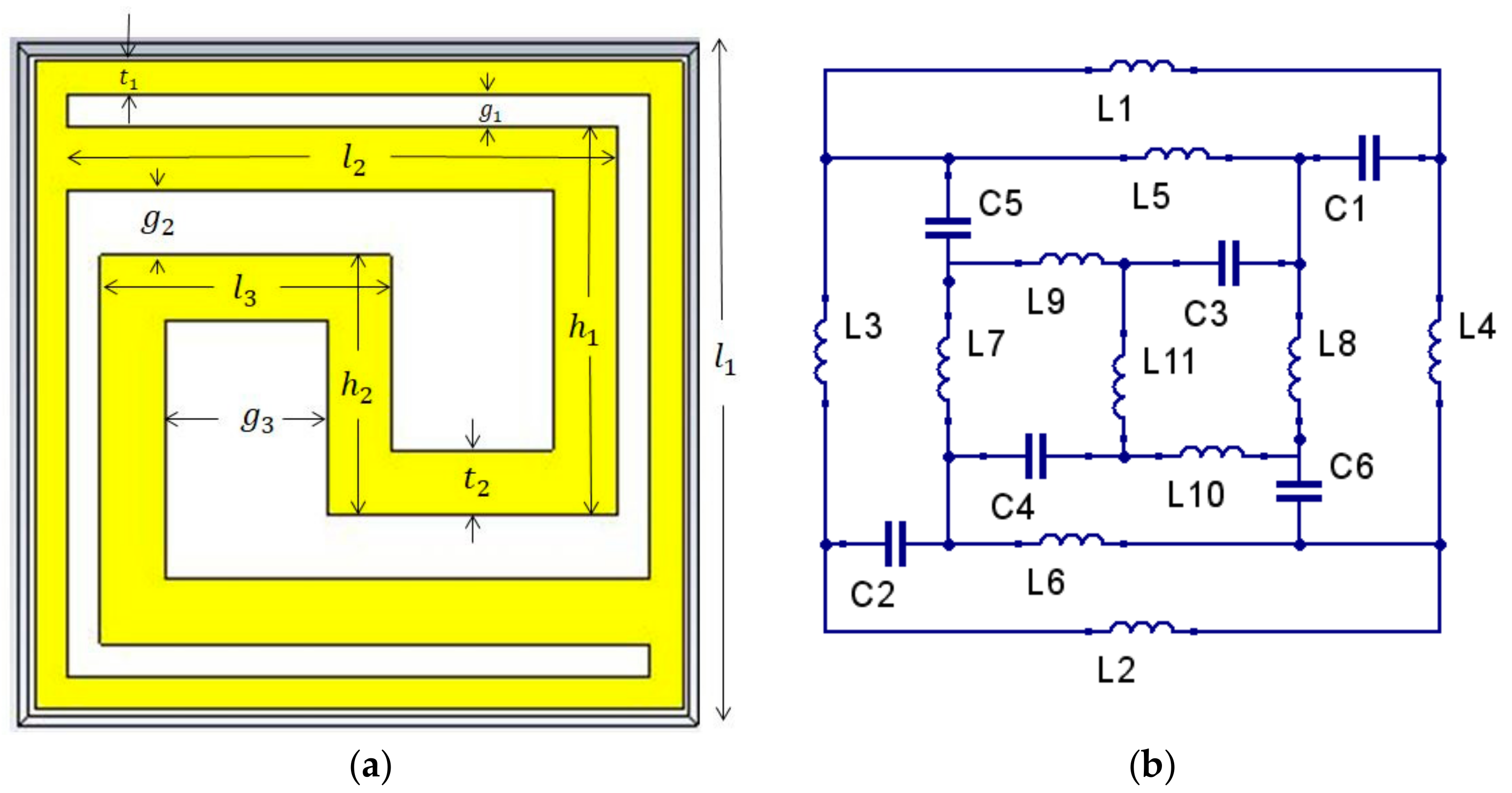
| Parameter | l1 | l2 | l3 | h1 | h2 | t1 | t2 | g1 | g2 | g3 |
| Size (mm) | 10 | 8.5 | 4.5 | 6 | 4 | 1 | 1 | 0.5 | 1 | 2.5 |
| Band | Ku Band (12–18) | K Band (18–26.5) | ||
|---|---|---|---|---|
| Frequency | 15.3 GHz | 17.04 GHz | 20.06 GHz | 21.3 GHz |
| Permittivity | −0.6466 | −0.4076 | −0.1 | 0.8337 |
| Permeability | −1.009 | −0.1276 | 2.252 | −1.352 |
| Refractive Index (NRW) | −0.9062 | −0.4373 | −0.5395 | −0.3514 |
| Refractive Index (DRI) | −0.9062 | −0.4373 | 0.5395 | 0.3514 |
| Absorption | 0.9804 | 0.8893 | 0.8593 | 0.8668 |
| Polarization Angle | Frequency Band | Resonance Frequency (GHz) | Max Absorption (%) | EM Mode | Substrate | Dielectric Constant | |||
|---|---|---|---|---|---|---|---|---|---|
| 0 | Ku | 15.3 17.04 | 98.04 88.93 | −0.6466 −0.4076 | −1.009 −0.1276 | −0.9062 −0.4373 | TEM | FR4 | 4.6 |
| K | 20.06 21.3 | 85.93 86.68 | −0.1 0.8337 | 2.252 −1.352 | −0.5395 −0.3514 | ||||
| 40 | Ku | 15.29 17 | 97.85 85.34 | −0.7707 −0.2505 | −0.8825 −0.772 | −0.8786 −0.4528 | |||
| K | 20.02 21.24 | 99.95 81.76 | −0.1067 −0.1156 | 0.206 0.8697 | −0.2 −0.3296 | ||||
| 80 | Ku | 15.29 16.97 | 97.85 80.28 | −0.7699 −0.108 | −0.8829 −1.779 | −0.8785 −0.4846 | |||
| K | 19.75 21.24 | 80.16 81.81 | 0.7407 −0.1162 | −1.907 2.261 | −0.3075 −0.3302 |
| Polarization Angle | Frequency Band | Resonance Frequency (GHz) | Max Absorption (%) | EM Mode | Substrate | Dielectric Constant | |||
|---|---|---|---|---|---|---|---|---|---|
| 0 | Ku | 14.64 | 83.25 | −6.39 | 5.674 | −2.381 | TEM | Rogers 3035 | 3.5 |
| K | 18.24 21.2 24.62 26.15 | 94.43 92.92 83.71 93.55 | −1.195 −2.957 −4.03 −1.002 | −1.064 −9.058 −1.505 −3.073 | −1.224 −4.908 −2.983 −1.604 | ||||
| 40 | Ku | 14.64 | 83.26 | −6.39 | 5.674 | −1.383 | |||
| K | 18.24 21.2 24.62 26.15 | 94.42 92.92 83.72 93.55 | −1.195 −2.957 −4.029 −1.003 | −1.064 −9.058 −1.503 −3.073 | −1.224 −2.4 −2.982 −1.604 | ||||
| 80 | Ku | 14.64 | 83.25 | −6.39 | 5.674 | −1.382 | |||
| K | 18.24 21.2 24.62 26.15 | 94.43 92.92 83.69 93.54 | −1.195 −2.957 −4.029 −1.002 | −1.064 −9.058 −1.503 −2.495 | −1.224 −4.908 −2.981 −1.604 |
| Polarization Angle | Frequency Band | Resonance Frequency (GHz) | Max Absorption (%) | EM Mode | Substrate | Dielectric Constant | |||
|---|---|---|---|---|---|---|---|---|---|
| 0 | Ku | 15.04 | 89.77 | −5.668 | 8.465 | −2.459 | TEM | Rogers 4003 | 3.38 |
| K | 22.17 25.46 26.88 | 93.28 93.72 92.87 | −1.733 −2.896 −0.7353 | −7.304 −1.918 −2.112 | −4.914 −2.659 −1.481 | ||||
| 40 | Ku | 15.04 | 89.78 | −5.664 | 8.462 | −2.461 | |||
| K | 22.17 25.46 26.88 | 93.28 93.72 92.87 | −1.733 −2.896 −0.7353 | −7.304 −2.078 −2.112 | −4.914 −2.659 −1.481 | ||||
| 80 | Ku | 15.04 | 89.78 | −5.663 | 8.462 | −2.461 | |||
| K | 22.17 25.46 26.88 | 93.28 93.72 92.87 | −1.733 −2.896 −0.7353 | −7.304 −2.078 −2.112 | −4.914 −2.659 −1.481 |
| Ref. # | Year | Size (mm) [Unit Cell] | Substrate Material | Used Frequency Bands | Max Absorption | Application | Resonance Frequency (GHz) |
|---|---|---|---|---|---|---|---|
| Sim et. al. [29] | 2017 | 16.8 × 16.8 | FR4 | X and Ku | >80% | Not specified | 11, 12, 13, 14, 15 |
| Madhav et. al. [30] | 2018 | 40 × 40 | FR4 | Ku, K, and Ka | Not shown | Not specified | 1.9, 7.3, 17.8, 25 |
| Khan et. al. [31] | 2018 | 10 × 10 | RO4350B | X and Ku | Not shown | Hollow waveguide filter and perfect absorber | 7.82, 9.65 |
| Agrawal et. al. [32] | 2018 | 18 × 18 | FR4 | X and Ku | 99.9% | Not specified | 7.6, 8.9, 12.3, 12.8 |
| Jafari et. al. [33] | 2019 | 24 × 24 | FR4 | X and Ku | >84% | Not specified | 8.6, 10.2, 11.95 |
| Our proposed work | 2019 | 10 × 10 | FR4RT 3035RT 4003 | Ku and K | 99.95% | Perfect Absorber | 14.64–15.3, 17.04–18.24, 20.06–21.3, 24.62–26.88 |
© 2019 by the authors. Licensee MDPI, Basel, Switzerland. This article is an open access article distributed under the terms and conditions of the Creative Commons Attribution (CC BY) license (http://creativecommons.org/licenses/by/4.0/).
Share and Cite
Hannan, S.; Islam, M.T.; Hoque, A.; Singh, M.J.; Almutairi, A.F. Design of a Novel Double Negative Metamaterial Absorber Atom for Ku and K Band Applications. Electronics 2019, 8, 853. https://doi.org/10.3390/electronics8080853
Hannan S, Islam MT, Hoque A, Singh MJ, Almutairi AF. Design of a Novel Double Negative Metamaterial Absorber Atom for Ku and K Band Applications. Electronics. 2019; 8(8):853. https://doi.org/10.3390/electronics8080853
Chicago/Turabian StyleHannan, Saif, Mohammad Tariqul Islam, Ahasanul Hoque, Mandeep Jit Singh, and Ali F. Almutairi. 2019. "Design of a Novel Double Negative Metamaterial Absorber Atom for Ku and K Band Applications" Electronics 8, no. 8: 853. https://doi.org/10.3390/electronics8080853
APA StyleHannan, S., Islam, M. T., Hoque, A., Singh, M. J., & Almutairi, A. F. (2019). Design of a Novel Double Negative Metamaterial Absorber Atom for Ku and K Band Applications. Electronics, 8(8), 853. https://doi.org/10.3390/electronics8080853