Abstract
Due to the increasing defect rates in highly scaled complementary metal-oxide-semiconductor (CMOS) devices, and the emergence of alternative nanotechnology devices, reliability challenges are of growing importance. Understanding and controlling the fault mechanisms associated with new materials and structures for both transistors and interconnection is a key issue in novel nanodevices. The graphene nanoribbon field-effect transistor (GNR FET) has revealed itself as a promising technology to design emerging research logic circuits, because of its outstanding potential speed and power properties. This work presents a study of fault causes, mechanisms, and models at the device level, as well as their impact on logic circuits based on GNR FETs. From a literature review of fault causes and mechanisms, fault propagation was analyzed, and fault models were derived for device and logic circuit levels. This study may be helpful for the prevention of faults in the design process of graphene nanodevices. In addition, it can help in the design and evaluation of defect- and fault-tolerant nanoarchitectures based on graphene circuits. Results are compared with other emerging devices, such as carbon nanotube (CNT) FET and nanowire (NW) FET.
1. Introduction
The development of deep submicron complementary metal–oxide–semiconductor (CMOS) technology includes the possibility of ultrasmall, low-power electronic products, such as communication and computing devices, embedded sensors, etc. However, in addition to the benefits of smaller transistors, there are significant problems in shrinking conventional devices to the nanoscale. They are mainly as follows [1,2]:
- Device fabrication. It may be difficult to extend optical lithography into the realm of low tens of nanometers. Furthermore, random process variations can lead to device characteristics that are unpredictable.
- Device operation. As dimensions are reduced, voltage levels also need to be reduced accordingly. This fact increases the subthreshold static power of the metal–oxide–semiconductor field-effect transistors (MOSFETs). In addition, conventional MOSFETs will behave differently, appearing quantum effects, such as tunneling and ballistic transport.
- Heat dissipation. As device density increases, heat dissipation becomes a major problem, reducing circuit reliability and leading to shorter device lifetimes, or even to device failure.
Recent proposals for sub-10 nm integrated circuit (IC) technologies show many challenges [3]. New transistors and interconnect materials, new mask making and patterning techniques, and novel defect inspection methods are necessary to cope with those extremely small sizes. In addition, fundamental physical limitations related to quantum tunneling are increasingly important.
Given the preceding problems, the electronic industry has begun to look beyond shrinking the size of conventional electronic devices. New devices and system architectures will need to be developed, based on physical effects only encountered on the nanoscale. A wide set of emerging logic nanodevices beyond silicon transistors have been proposed, based on new state variable definitions, structures, or materials [4].
Among them, the most promising in the near future are carbon nanotube (CNT) FET, nanowire (NW) FET, tunnel (T) FET, and graphene nanoribbon (GNR) FET [5]. They present a conventional MOSFET-like structure, and the logical state is based on electronic charge.
This paper is dedicated to GNR FETs, due to the excellent electrical and thermal properties of graphene [6,7,8]. Since its discovery in 2004, no material has attracted more attention than graphene. In particular, its high carrier mobility due to the room temperature ballistic transport of charge carriers offers a big potential capability to design high speed logic circuits. In addition, the outstanding thermal properties of graphene provide good perspectives to cope with the increasing dissipation power density of integrated circuits. Moreover, the potential to apply full planar processing for devices promises high integration with conventional CMOS fabrication processes [9,10,11,12].
Besides the excellent properties of graphene, it presents a big challenge for digital logic applications. It is a semi-metal with zero bandgap. Patterning narrow stripes of graphene (GNR) results in the quantum confinement of carriers in 1D armchair-GNR (A-GNR), which can open a bandgap of several hundred meV in order to fulfill the requirements of low-power logic design [13,14]. Nevertheless, narrow GNRs of a few nanometers presents reliability challenges related to edge roughness and dimension variations, which can affect the electronic properties of GNR FETs [15,16,17].
In fact, reliability is expected to become a big issue in emerging nanodevices, due to scaling and the use of new materials and designs. Important reliability challenges are as follows [2]: 1. Understanding and modeling failure mechanisms; 2. Analyzing the impact on circuits; and 3. Introducing reliability evaluation methodologies.
This paper tries to cover these challenges, applying them to GNR FETs. Figure 1 summarizes the methodology devised. In a first step, relevant manufacturing defects and variations are reviewed from the literature on GNR FET devices. Then, the resulting fault propagation is analyzed to deduce fault models at the device and logic circuit levels.
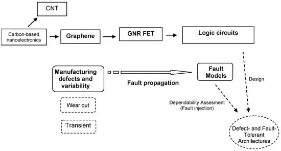
Figure 1.
Planned methodology in our work.
Fault models at the logic level have been generated from the structure of logic circuits made of transistors. These fault models, which constitute the main contribution of this paper, will enable the future development and precise evaluation of new defect- and fault-tolerant architectures for nanoelectronic systems. Injection of the fault models can be a powerful technique to carry out the evaluation of the system, while doing it at a manageable cost. Wear-out (aging) and transient faults are also important issues that must be deeply analyzed in future research.
In previous studies, we applied the methodology shown in Figure 1 to other emerging devices such as NW FETs and CNT FETs [18,19,20]. In this way, this paper completes a sort of trilogy of promising logic nanodevices. Note that our work is based on a qualitative analysis of fault propagation, using the equations of the devices and the structure of the logic circuits. Other research papers in the literature [21,22,23] have applied simulations at physical and electronic (SPICE) levels in a more quantitative approach. These two types of analysis may complement each other.
In summary, the main contributions of our paper are as follows:
- Identifying a wide set of fault causes and mechanisms in GNR FET devices. This constitutes a deep review task, necessary to develop points 2 and 3.
- Analyzing the fault propagation and modeling faults at the logic level. This phase is done based on the previous point, and the structure and equations of digital circuits. Fault modeling opens the possibility of evaluating the reliability of defect-tolerant nanoarchitectures by means of fault injection at a manageable cost.
- Comparing the fault models with other emerging devices, namely, CNT FETs and NW FETs. They are also promising devices for future digital applications.
This work is organized as follows. Section 2 and Section 3 present a brief description of GNR FET devices and logic circuits in current technology. Section 4 reviews some key reliability challenges and requirements related to emerging nanodevices, structures, and materials beyond CMOS. Section 5 presents a survey of fault causes and mechanisms, which leads to the identification of fault models at the device and circuit levels. Finally, Section 6 provides some conclusions and proposals for future work.
2. Graphene Nanoribbon Devices
As mentioned above, GNR FETs are one of the most promising devices for digital logic [4]. The main challenge of GNR FETs is the desired combination of sufficient bandgap and enough mobility.
Graphene must be processed into narrow strips (GNRs) with widths below 10 nm in order to open a sufficient bandgap and become semiconducting. GNR bandgap is inversely proportional to its width [6].
Figure 2 shows the structure of a wide-narrow-wide (WNW) all-graphene dual-gated GNR FET [7]. The wide regions are metallic and the narrow ones are semiconducting. A planar top metal gate modulates the channel conductance, while a substrate acts as a back gate for electrostatic channel doping. The device has an almost conventional MOSFET structure, but with an alternate channel material (GNR) to enhance the charge transport.
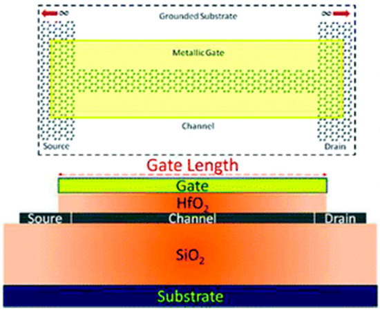
Figure 2.
Graphene nanoribbon field-effect transistor (GNR FET). Top view and side view [10]. Copyright.
Notice that the GNR has armchair edges. Armchair GNRs can be semiconducting or metallic, depending on the ribbon width. By contrast, zigzag GNRs demonstrate metallic properties. Using an all graphene device/interconnect circuit topology would benefit from ohmic contacts, and it would reduce extrinsic capacitance and circuit level delay [7]. Forming good graphene–metal contacts is a critical issue in graphene circuits [2,4].
3. Graphene Nanoribbon Logic Circuits
In this section we show some examples of logic circuits based on GNR FET devices. Most of the logic circuits proposed in the literature [2,10,13,21,23,24] present a CMOS-like structure. They are basic logic gates or memory cells.
Figure 3a illustrates an inverter, the simplest logic element. This inverter design uses the WNW (metal–semiconductor–metal) all-graphene model for pull-up (PUN) and pull-down (PDN) networks. Notice that CNT (carbon nanotube) can make direct contact with the device-level graphene. This improves the interconnects, due to the room temperature ballistic transport of charge carriers in the CNT.
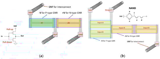
Figure 3.
Examples of GNR FET logic gates [10]: (a) NOT. (b) NAND. Copyright.
On the other hand, Figure 3b shows a NAND logic gate. Pull-up transistors are connected in parallel, whereas pull-down transistors are connected in series. A CMOS-like structure ensures that static power remains near zero.
Graphene has also been used in non-volatile flash memory cells, replacing the floating gate of the cells [25]. Likewise, it can be employed as conductive channels in bit lines and word lines of the memory. The use of graphene in non-volatile memories presents fewer challenges than in logic gates, because memory operation requires only large (>104) Ion/Ioff without need for Av (voltage gain) >1 [24].
As a last example, latches and static RAM (SRAM) cells have also been proposed [18,26,27]. They are mainly based on a typical cross-coupled inverter structure, where inverters are designed from GNR FETs.
4. Reliability Challenges and Requirements
Reliability is a big issue in emerging nanodevices, because a high rate of manufacturing defects and variations are expected [2,4,24].
The speed of the introduction of new materials and devices is exceeding our capability to build up learning on new failure mechanisms and physics, whereas the fault rate requirements are becoming increasingly demanding. Moreover, this is complicated by the fact that new failure physics may lead to significant and important deviations from the traditional statistical distributions, making error analysis non-straightforward [2].
The study of fault causes and mechanisms is necessary to achieve fault prevention in the design process, as well as the proper fault tolerance techniques. In addition, the gap between device reliability and system reliability is very large. There is a strong need for device reliability investigation to address the impact on circuits. Work is needed on rapid characterization techniques, validated models, and design tools for each failure mechanism [2,28].
Another important requirement is to apply an efficient reliability evaluation methodology [2], which can deliver relevant long-term degradation assessment while preventing excessive accelerated testing which may produce misleading results. This need is driven by the decreasing process margin and increasing variability, which greatly degrades the accuracy of lifetime projection from a standard sample size. The ability to stress a large number of devices simultaneously is highly desirable, particularly for long-term reliability characterization. Doing it at a manageable cost is a challenge that is very difficult to meet, being more difficult as we migrate to more advanced technology nodes. Fault injection techniques may be straightforward at this point. Other techniques based on physical simulation [9] and probabilistic models [29] have also been proposed.
It is commonly thought that the ultimate nanoscale device will have a high degree of variation and a high percentage of non-functional devices right from the start. This is viewed as an intrinsic property of devices at the molecular scale. As a result, for the designer, it will no longer be possible to take into account a “worst-case” design window, because this would jeopardize too much the performance of the circuits. To deal with this situation, a complete paradigm change in circuit and system design will therefore be needed [2,4]. While we are not there yet, the increase in variability is clearly already a reliability problem that is taxing the ability of most manufacturers. This problem is provoked by the variability that degrades the accuracy of lifetime projection, forcing a dramatic increase in the number of devices tested. The coupling between variability and reliability is squeezing out the benefit of scaling. At some point, perhaps before the end of the roadmap, the cost of ensuring each of the transistors in a large integrated circuit to function within specification may become too high to be practical. As a result, the fundamental philosophy of how to achieve product reliability may need to be changed. This concept is known as resilience, that is, the ability to cope with stress and catastrophe. One potential solution would be to integrate the so-called knobs and monitors in sensors of other circuit parts that are running out of performance and then, during runtime, they can change the biasing of the circuits. Such solutions need to be further explored and developed. Ultimately, circuits that can dynamically reconfigure themselves to avoid failing and failed devices (or to change or improve functionality) will be needed. Sophisticated defect- and fault-tolerant techniques must be introduced [30].
In this way, Figure 4 summarizes some key reliability challenges and requirements of emerging nanodevices and nanoarchitectures. In this paper, we focused on the three first requirements, emphasized in bold type: (1) understanding fault causes and mechanisms; (2) analyzing the impact on logic circuits; and (3) generating fault models easy to inject at a manageable cost.
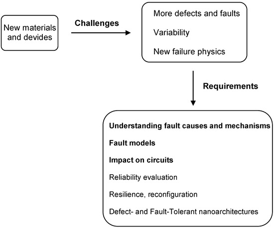
Figure 4.
Reliability challenges and requirements of emerging nanodevices and nanoarchitectures.
The design and evaluation of new defect- and fault-tolerant nanoarchitectures represent a challenging future research subject.
5. Fault Causes, Mechanisms, and Models
This section examines fault causes and mechanisms of GNR FETs, which leads to the identification of fault models at the device and logic circuit levels. Fault causes and mechanisms were extracted doing a literature review. A summary is shown in Table 1 and Figure 5. References are indicated in the text.

Table 1.
Fault causes, mechanisms, and models of GNR FET logic circuits.
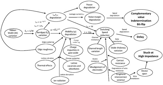
Figure 5.
Fault propagation graph for GNR FET logic circuits.
As presented in Table 1, although the biggest part of the study focused on manufacturing defects and variations, some environment- and aging-related faults were also treated. We generated the fault models in two steps:
- Study of the impact of defects and faults on GNR FETs. Generation of fault models at the device (transistor) level. In this step, we analyzed the equations of the devices and their parameters.
- Study of fault propagation from the device level to the (logic) circuit level. Generation of fault models at the logic circuit level. This step is based on the structure of logic circuits made of transistors.
Figure 5 shows the fault propagation process in a directed graph. The graph displays fault causes and mechanisms, and how they affect some key parameters: energy bandgap, mobility, Ion/Ioff, noise margin, etc. Fault models are highlighted at the end nodes of the graph.
Next, we explain the details of the fault model generation.
5.1. Manufacturing Variations
Some parameters of the transistors are affected by manufacturing variations. Next, we describe the most important variations and their impact on the characteristics of transistors and logic circuits.
5.1.1. Ribbon Width
Ribbon width variation is a critical defect that may provoke an important degradation in power, noise margin, and speed. Notice that the word “degradation” does not mean a change over time, because the faults are permanent. In fact, “degradation” implies a change in the spatial domain.
Let us analyze the influence on each factor.
- Power degradation. GNR FET ON current scales proportionally with width W, whereas the OFF current has an exponential dependency [10]:where: Eg = GNR bandgap, K = Boltzmann constant, T = temperature.
Given that the GNR bandgap is inversely proportional to its width [7], we obtain the following:
Then Ioff can be written in function of W as follows:
where C = constant.
To achieve manageable OFF currents for digital applications, GNR widths must be scaled within the sub-10 nm regime to avoid the increase in static power dissipation and poor ON–OFF ratio.
Important variations in the power (mainly static) of an inverter gate have been observed in simulation experiments [9,21,23,31].
- Noise margin degradation. The second effect is a significantly diminishing noise margin. Band-to-band tunneling in narrow bandgap GNR FETs prevents either PUN or PDN of logic circuits from completely cutting off when its complement network is active [10]. This may lead to voltage variations in the output of logic circuits. We propose complementary value and indetermination fault models for combinational circuits. The complementary value model means a change in the logic value (“0” changes to “1” or vice versa). The indetermination model represents a value that is in the forbidden gap between “0” and “1” logic values. In the case that the perturbed signal arrives at a sequential circuit, it can propagate and manifest as a bit-flip, which means a change in the memory state.
Noise margin degradation can perturb the state of latches [9,21] and SRAM memories [27]. Dense memories, which are a big prospect for graphene-based devices, can be particularly susceptible to variations and defects with near-zero noise margins, as well as an increase in leakage power [31].
Note that a dash line appears in the “Fault Model at Device Level” column in Table 1. This is because there are no standard fault models at the device level (stuck-on, stuck-off, delay) related to Ion/Ioff degradation.
- Speed degradation. W variations can provoke the mobility degradation of the carriers, and thus the reduction of the GNR FET switching speed. Let us analyze this relationship. First, the ribbon width affects the energy bandgap according to Equation (3). Then, the mobility µ depends on Eg using the following expression [10]:where:
- λsc = scattering length,
- m* = effective mass,
- m*v = ℏkF = carrier momentum,
- ℏ = h/2π = reduced Planck constant,
- kF = Fermi wavenumber.
From Equations (3) and (5), the mobility depends on the ribbon width as follows:
Increasing the ON–OFF ratio by reducing W is predicted thereby to reduce the mobility. Moreover, variations of W have more impact on µ for thinner ribbons, due to the square root relationship. In fact, we observe the following:
Finally, the connection with the switching speed comes from the time required for a carrier to travel across the ribbon channel of the GNR FET. This delay depends on the mobility as follows [32]:
where E = electric field across the channel.
Then, from Equation (6), the dependency of τ with W is given by the following:
In this way, reducing W leads to a degradation of the switching speed at the transistor level. Furthermore, this degradation is greater for thinner ribbons.
Delay at the device (transistor) level propagates to the logic level (see Table 1), provoking the performance degradation of the logic circuits that are made of GNR FETs. The delay model is suggested, which means a degradation of the propagation delay of the transistors and the digital circuits.
Important variations in the delay of an inverter gate have been observed in simulation experiments [21,23]. The delay increases notably as the width of the GNR decreases.
Another factor that is affected by W variations is Ion current, as shown by Equation (1). Reducing channel width decreases Ion and this worsens delay again. It is common to put several parallel semiconducting GNRs in order to increase Ion and to improve the delay of the transistor [10]. Nevertheless, multiple defects and variability can happen in various GNRs simultaneously, provoking much more impact than single faults [21].
5.1.2. Oxide Thickness
Oxide thickness variations modify the gate (oxide) capacitance Cox and, subsequently, the intrinsic capacitance of the GNR FET:
where CQ is the quantum capacitance [10].
Propagation delay of digital circuits is proportional to CIN, so oxide thickness variations can provoke variations in the speed of digital circuits. The delay model is proposed to represent this effect.
5.1.3. Channel Length
The time required for carriers to travel the transistor channel depends on the channel length (or gate length) LG as follows [32]:
where VD = drain voltage.
Variations in LG may change the channel resistance. They have an important impact on the speed of transistors and, consequently, of digital circuits. Moreover, the ballistic transport of the GNR FET can be degraded, if LG is higher than the mean free path for elastic and inelastic collisions of electrons [1].
The delay model should also be representative for this case.
Furthermore, the cutoff frequency of graphene transistors depends on LG as fT = (LG)−2 [32], and thus, it can be affected by the channel length variations. This can be problematic in the design of graphene-based electronics for high-frequency applications.
5.1.4. Misalignment of Electrodes
Misalignment of drain, source, and gate electrodes can provoke significant gaps between electrodes, where a large proportion of the graphene channel in the gap area is not gated. This increases the access resistance and may lead to delay and performance degradation. The delay fault model is again chosen for this fault.
An approach to the fabrication of high-speed graphene transistors with a self-aligned nanowire gate to prevent such degradation is proposed in [33].
5.2. Manufacturing Defects
5.2.1. Edge Roughness
Currently, line edge roughness along a GNR edge is an unavoidable consequence of lithographic and chemical fabrication techniques. State-of-the art etching techniques are far enough from atomistic resolution. This leads to conductive channels having irregular edges. Random edges may lead to additional scattering, which can be detrimental for the speed and energy consumption of transistors, and in fact, they can diminish the advantages offered by graphene’s ballistic transport [7,12].
Scattering length can include edge roughness, charge impurities, and phonons [10]:
Intrinsic device level scattering mechanisms can influence mobility and transit time (see Equations (5) and (8)), and thus the delay model is adequate to represent this effect.
In addition, simulations in [9,23,31] have shown that edge roughness effects reduce Ion and increase Ioff, with the effect of edge roughness increasing as GNR width is decreased. Ion/Ioff degradation provokes a worst power and noise margin, as shown in Figure 5 and Table 1. As commented before, this may manifest as complementary value, indetermination, or bit-flip fault models at the logic level.
Edge roughness is projected to play an important role in GNR FET behavior.
5.2.2. Charge Impurities
Recent experimental studies suggest that transport in graphene nanoribbon is greatly affected by defects at the edges and charged impurities [2].
Top-gated graphene devices allow the fabrication of independently addressable device arrays, as well as more complex integrated devices and circuits. However, the deposition of dielectric can introduce undesired impurities or vacancies in the graphene lattice, leading to a significant degradation in carrier mobilities [34]. Exploring graphene for future electronics requires the effective integration of high-quality gate dielectrics.
In [32], top-gated graphene transistors operating at high frequency (gigahertz) were fabricated and their characteristics analyzed. After deposition of top gate dielectrics by atomic layer deposition (ALD), there was a significant reduction in both the device conductance and mobility. The current and mobility degradation in the oxide-covered devices may be attributed to charged impurity scattering associated with the NO2 functionalization layer and interface phonon scattering in the oxide.
Charge impurities are one of the intrinsic scattering mechanisms, as is shown in Equation (12). From this point of view, the delay fault model is suitable to represent the fault effect at the transistor and logic circuit levels.
It has been observed that charged impurities severely affect the Schottky barrier at the source end of the transistor channel [21,23]. Charged impurity increases the barrier height and thickness, the electron flow is significantly reduced by the large barrier, and the ON current is notably reduced. Delay, power, and noise margin degradation have been observed in the simulations of a logic inverter.
As mentioned previously, this may manifest as complementary value, indetermination or bit-flip fault models at the logic level.
When simultaneous variations in width and charge impurities are considered, variations in width are predominant, although the effects are exacerbated by the presence of charged impurities [9,31]. In addition, multiple defects in an array of parallel GNR channels can occur. For example, if the pitch (the spacing between the neighboring GNRs) is comparable to the gate oxide thickness, it is reasonable to expect an impurity to affect more than one GNR in the GNR FET channel, because the charged impurity’s electric field is not completely screened by the gate.
5.2.3. Lattice Vacancies and Adsorbates
During the fabrication process, carbon atom vacancies in the interior of the ribbon may be introduced. In addition, adsorbed atoms and molecules (e.g., H, F, O, and OH) bond covalently to graphene and disrupt the lattice symmetry [10,35]. Both are possible candidates for the imperfections that scatter electrons passing through the ribbon. This type of scattering is elastic and similar to impurities scattering, and results in low electron transmission probabilities and the decay of the ballistic quantum conductance [1]. Scattering also degrades the charge mobility, as is show in Equation (5). The increase of the ribbon resistance and the mobility degradation worsen the transit time, and thus the delay model is chosen to represent this effect.
5.2.4. Electrical Contacts
Forming good metal–graphene contacts remains a critical research issue [4,12,36]. Contact resistance needs to be improved in current technology. Nevertheless, ohmic contact formation may be easier than in small diameter carbon nanotubes, which tend to create Schottky barriers. GNR circuits can avoid this problem by using the same sheet of graphene for both active devices and interconnect [10]. The width-dependent conductivity allows the design of a monolithically patterned wide-narrow-wide (WNW) all-graphene interconnect–channel heterostructure, as shown in Figure 2. However, metal contacts are unavoidable at the ends of the device array, due to topological requirements for connecting complex circuit elements. The improvement of electrical contacts between nanoobjects and electrodes can be done by applying ultrasonic bonding [37,38].
Metallic contact resistance affects the switching speed of logic circuits, and they should be modelled with the delay fault model.
5.3. Environmental Faults
5.3.1. Ion Radiation
Defects in crystalline lattice may be produced by ion radiation. Ion damage depends on penetration depth and cascade effects [10]. Cascade effects occur when a scattered C atom with a large amount of energy hits and perturbs another C atom iteratively. If ion dose is low, only a few lattice atoms are perturbed. High ion doses produce full lattice disorder. This leads to a wear-out process. Lattice disruption can provoke the mobility degradation of electrons and the speed degradation of transistors. The delay fault model is proposed to represent this situation.
5.3.2. Thermal Effects
Thermal effects increase the inelastic electron–phonon collisions, since phonon (quantized lattice vibrations) energy will be greater at higher temperatures. The lattice vibrates more at higher temperatures. This may provoke a degradation of mobility and speed, thus leading to the delay fault model.
Furthermore, thermal effects play an important role in the phase coherence of the electron wave function:
As temperature T increases, the spread of electron energies (that vary on the order of KT) will increase, along with their associated phase differences, eventually leading to thermal decoherence even in the absence of particle scattering [1]. Decoherence is one of the most problematic issues facing the development of quantum computers. That is, the computation must be finished before the quantum state decoheres. Quantum computing is out of the scope of this paper, so no fault model is proposed for this case.
5.4. Aging Faults
Graphene Interconnection Defects
It has been observed that graphene wires degrade with time under constant current stress, mainly caused by the formation of defects due to graphene oxidation [39]. This provokes a linear increase of the wire resistance with time before the final breakdown. The increase of the wire resistance can affect the device switching delay, and thus, the delay model is proposed to represent this class of fault. Breakdown can be modelled as the open (or stuck-off) of the device, and this can provoke a fixed or floating value in the logic circuit, depending on which transistor (N, P, or both) fails. Therefore, stuck-at and high impedance may be suitable fault models at the logic abstraction level.
5.5. Summary
From the previous study, we can highlight some aspects:
- Fault causes have been classified in four groups (see Table 1): manufacturing variations, manufacturing defects, environmental faults and aging faults. The most harmful causes according to the literature are ribbon width variations, edge roughness, and charge impurities in gate oxide.
- Two main types of fault mechanisms have been identified (see Figure 5): those that perturb the logic signal value and those that impact the logic signal timing. The former are related to Ion/Ioff degradation and some aging processes, whereas the latter are linked with mobility degradation.
- With respect to fault models at the device level, we note that the most frequent is the delay fault model (see Table 1). This is because there is no standard fault model (stuck-on, stuck-off, delay) related to Ion/Ioff degradation at the device level. In this case, a dash appears in the table. Nevertheless, stuck-off related to wire breakdown has been identified.
- Directly related to the fault mechanisms, two groups of fault models are proposed at the logic level. Timing degradation can be modelled with the delay fault model. Value degradation can be modelled with several fault models: complementary value and indetermination in combinational circuits, and bit-flip in sequential circuits and memory. Complementary value, indetermination and delay are permanent faults, whereas bit-flip is transient. Other fault models that affect the output value are stuck-at and high impedance, related to the breakdown of graphene wires. Table 1 and Figure 5 show that timing degradation and the delay fault model are quite relevant, because they are related to more fault causes.
- Obtained fault models are classic well-known ones. The reason for this is twofold: GNR FETs are charge-based electronic devices with a conventional MOSFET-like structure [4] and GNR FET logic circuits present CMOS-like structures (see Figure 3).
- Note that manufacturing defects and variations are permanent faults in essence. Nevertheless, environmental and wear-out faults can provoke aging processes, where the device characteristics change over time. Even transient faults may be generated by environment, although this is a subject of future research. The term “degradation” related to permanent faults implies an alteration in the spatial domain.
6. Comparison with CNT and NW Circuits
The objective of this section is to compare the fault models of GNR FET logic circuits with those based on other promising devices, namely, carbon nanotube (CNT) FETs and nanowire (NW) FETs. Details about the fault models for these devices can be found in our previous work [19,20].
6.1. Comparison with CNTs
Some harmful fault causes and mechanisms in CNT FET circuits are as follows:
- Manufacturing defects of the metallic and misalignment/misposition types [20]. The manufacturing process makes it nearly impossible to guarantee the perfect alignment and accurate positioning of all CNTs at the Very Large Scale Integration (VLSI scale, or the growing of semiconducting CNTs exclusively. GNR FET circuits avoid these defects, because graphene’s planar profile makes it amenable to well-established top-down planar fabrication techniques for silicon CMOS devices [40,41,42]. Some fault models, different from those of GNR FET circuits, have been identified in relation with metallic and misalignment/misposition defects. For instance, we note stuck-on/stuck-off at the device level, which may manifest as stuck-at or even a change in the logic function at the logic level [20,29].
- Producing a good electrical contact between CNTs and metal electrodes can be problematic, because they tend to create Schottky barriers. Although electrical contacts also remain an important issue in graphene circuits, GNR metal–semiconducting junctions can be patterned together into all-graphene circuits (see Figure 2), avoiding metallic contacts to some extent. Moreover, GNR–CNT junctions are possible, as shown in Figure 3. Poor contacts in CNT circuits provoke an increase of the device resistance. They can be modelled with the delay fault model [20]. Defective metallic contacts in GNR circuits are also modelled with the delay fault model (see Figure 5 and Table 1).
Other causes and mechanisms in CNT FET circuits are as follows:
- 3.
- Manufacturing variations, which affect some parameters of the CNT FET. Variations in the dimensions of the devices (CNT diameter, length, and oxide thickness) can modify the channel resistance and the threshold voltage of the transistor. This degrades the circuit speed. Thus, the delay fault model is proposed. As we have seen in Section 5, manufacturing variations are a critical issue in GNR FETs, especially ribbon width variation.
- 4.
- The break probability in CNT is very low, due to its high flexibility and fracture strain. Nevertheless, some research papers have studied the fracture mechanism in small diameter (less than 5 angströms) CNTs due to deformation and bending [43]. Related fault models have been identified in [20]. The fracture of CNT provokes the opening of the CNT FET channel and can be modelled with the stuck-off fault model at the device level. This may manifest as stuck-at or high impedance (open) at the logic level. About GNR, extremely high Young’s modulus and excellent flexibility has been demonstrated [44]. Although the fracture process is similar to that occurred in carbon nanotube, the width of the GNR was found to have a slight effect on the fracture point. On the other hand, graphene wire degradation with time has been observed [39]. Under constant current, wire conductivity degrades linearly with time, similar to CNTs. This can be modelled with delay, stuck-at, or high impedance at the logic level, as shown in Section 5.4.
In summary, the principal challenge in GNR FET circuits is the opening bandgap. This can reduce the mobility and strongly affects circuit speed. Thus, the delay fault model is of paramount importance, as shown in Table 1 and Figure 5. CNT FETs do not have the bandgap issue, nor the edge roughness defect. Fault models in CNT circuits are more balanced between the timing and the value degradation [20].
6.2. Comparison with NWs
Some typical fault causes and mechanisms in NW devices and circuits are as follows: (1) nanowire defects (broken wires, poor contacts, doping variation); (2) cross-point defects in programmable logic array (PLA) architectures; and (3) bridging of adjacent nanowires [19]. They manifest as stuck-on, stuck-off, and delay at the device (transistor and diode) level. The propagation to the higher (logic) level leads to a set of fault models similar to those of the CNT circuits. Stuck-at, high impedance, complementary value, and delay have been identified as fault models at the logic level. The similarity with CNT comes from comparable fault mechanisms and the 1D structure of both CNT and NW devices. In fact, cross-point defects have also been shown in CNT non-volatile RAM [20].
To end this section, Table 2 summarizes the more relevant fault causes, mechanisms, and models of the three devices.
Table 2.
Fault causes, mechanisms, and models of GNR, CNT and NW logic circuits.
Notice that fault models are “classic” ones, and in some cases, they are coincident (especially between CNT and NW). This is due to the fact that, as mentioned previously, all devices have a conventional MOSFET-like structure and the logic state variable is based on electronic charge.
7. Conclusions
Graphene nanoribbon (GNR) FET is a promising technology to design emerging research logic circuits, due to its outstanding potential speed and power properties. Nevertheless, logic circuits are a big challenge in the applications of graphene technology, due to the opening bandgap issue. Moreover, reliability is an issue of growing importance in novel nanotechnology devices. This work presents a study of fault causes, mechanisms, and models at the device level, as well as their impact on logic circuits based on GNR FETs. From a literature review of fault causes and mechanisms, fault propagation was analyzed, and fault models were derived for device and logic circuit levels. Proposed fault models are simple and easy to implement in HDL languages. These fault models were compared with those of other emerging nanodevices, namely, carbon nanotube FETs and nanowire FETs. In this way, different mechanisms and models were identified.
This work may be useful for fault prevention in the design process of graphene nanodevices. In addition, it can help to evaluate defect- and fault-tolerant nanoarchitectures based on graphene. Injection of the fault models can be a powerful technique for evaluation at a manageable cost.
For future work, some extensions can be suggested: (1) a deeper study of the use of GNR FETs to design logic circuits; (2) a wider study of aging (wear out) and transient faults, as there is no substantial research on the impact of degradation on devices at circuit operation speed; and (3) the design and evaluation of defect- and fault-tolerant nanoarchitectures based on graphene devices.
Author Contributions
D.G.-T. wrote the first draft of this paper and he was responsible for conceptualization and methodology. J.G.-M., L.J.S.-A., and P.J.G.-V. assisted in the writing and reviewing of the final version, the project administration, and the funding acquisition.
Funding
This work was supported in part by the Spanish Government under the research project TIN2016-81075-R and by Primeros Proyectos de Investigación (PAID-06-18), Vicerrectorado de Investigación, Innovación y Transferencia de la Universitat Politècnica de València (UPV), under the project 200190032.
Conflicts of Interest
The authors declare no conflict of interest.
References
- Hanson, G.W. Fundamentals of Nanoelectronics; Pearson Prentice Hall: Upper Saddle River, NJ, USA, 2008. [Google Scholar]
- International Technology Roadmap for Semiconductors (ITRS) 2013. Available online: http://www.itrs2.net/2013-itrs.html (accessed on 3 July 2019).
- Schuegraf, K. Semiconductor Logic Technology Innovation to Achieve Sub-10 nm Manufacturing. IEEE J. Electron Devices Soc. 2013, 1, 66–75. [Google Scholar] [CrossRef]
- International Technology Roadmap for Semiconductors (ITRS) 2015. Available online: https://bit.ly/2xiiT8P (accessed on 3 July 2019).
- Das, S. Overview of Emerging Research Logic Devices. In Proceedings of the ITRS Architecture Workshop; Stanford University: Stanford, CA, USA, 2015. Available online: https://bit.ly/2KWCvrB (accessed on 3 July 2019).
- Novoselov, K.S.; Geim, A.K.; Morozov, S.V.; Jiang, D.; Zhang, Y.; Dubonos, S.V.; Grigorieva, I.V.; Firsov, A.A. Electric Field Effect in Atomically Thin Carbon Films. Science 2004, 306, 666–669. [Google Scholar] [CrossRef] [PubMed]
- Geim, A.K.; Novoselov, K.S. The Rise of Graphene. Nat. Mater. 2007, 6, 183–191. Available online: https://www.nature.com/articles/nmat1849 (accessed on 3 July 2019). [CrossRef] [PubMed]
- Wu, Y.; Farmer, D.B.; Xia, F.; Avouris, P. Graphene Electronics: Materials, Devices, and Circuits. Proc. IEEE 2013, 101, 1620–1637. [Google Scholar] [CrossRef]
- Choudhury, M.R.; Yoon, Y.; Guo, J.; Mohanram, K. Graphene Nanoribbon FETs: Technology Exploration for Performance and Reliability. IEEE Trans. Nanotechnol. 2010, 10, 7217–7736. [Google Scholar] [CrossRef]
- Raza, H. Graphene Nanoelectronics: Metrology, Synthesis, Properties and Applications; Springer: Berlin/Heidelberg, Germany, 2012. [Google Scholar]
- De Heer, W.A.; Berger, C.; Conrad, E.H.; First, P. Pionics: The Emerging Science and technology of Graphene-Based Nanoelectronics. In Proceedings of the 2007 IEEE International Electron Devices Meeting, Washington, DC, USA, 10–12 December 2007; pp. 199–202. [Google Scholar]
- Avouris, P. Graphene: Electronic and Photonic Properties and Devices. Nano Lett. 2010, 10, 4285–4294. [Google Scholar] [CrossRef]
- Banakadi, Y.M.; Srivaska, A. Scaling Effects on Static Metrics and Switching Attributes of Graphene Nanoribbon FET for Emerging Technology. IEEE Trans. Emerg. Top. Comput. 2015, 3, 458–469. [Google Scholar]
- Rodríguez, S.; Rusu, A.; de la Rosa, J.M. Overview of Carbon-Based Circuits and Systems. In Proceedings of the 2015 IEEE International Symposium on Circuits and Systems (ISCAS), Lisbon, Portugal, 24–27 May 2015; pp. 2912–2915. [Google Scholar]
- Avouris, P.; Cheng, Z.; Perebeinos, V. Carbon-based Electronics. Nat. Nanotechnol. 2007, 2, 605–615. [Google Scholar] [CrossRef]
- Banerjee, S.K.; Register, L.F.; Tutuc, E.; Basu, D.; Kim, S.; Reddy, D.; MacDonald, A.H. Graphene for CMOS and Beyond CMOS applications. Proc. IEEE 2010, 98, 2032–2046. [Google Scholar] [CrossRef]
- Schwierz, F. Graphene Transistors: Status, Prospects, and Problems. Proc. IEEE 2013, 101, 1567–1584. [Google Scholar] [CrossRef]
- Gil, D.; de Andrés, D.; Ruiz, J.; Gil, P. Identifying Fault Mechanisms and Models of Emerging Nanoelectronic Devices. In Proceedings of the 1st Workshop on Dependable and Secure Nanocomputing, IEEE International Conference on Dependable Systems and Networks, Washington, DC, USA, 25–28 June 2007; p. 288. Available online: https://bit.ly/2FOsnwH (accessed on 3 July 2019).
- Gil, D.; de Andrés, D.; Ruiz, J.C.; Gil-Vicente, P.; de Vera, C.N. Developing Fault Models for Nanowire Logic Circuits. In Proceedings of the 2nd Workshop on Dependable and Secure Nanocomputing, IEEE International Conference on Dependable Systems and Networks, Anchorage, AK, USA, 27 June 2008; pp. C6–C11. Available online: https://bit.ly/2LBBepk (accessed on 3 July 2019).
- Gil, D.; de Andrés, D.; Ruiz, J.C.; Gil-Vicente, P. Impact of Manufacturing Defects on Carbon Nanotube Logic Circuits. In Proceedings of the 3rd Workshop on Dependable and Secure Nanocomputing, IEEE International Conference on Dependable Systems and Networks, Lisbon, Portugal, 29 June 2009; Available online: https://bit.ly/2NrMMxR (accessed on 3 July 2019).
- Choudhury, M.; Yoon, Y.; Guo, J.; Mohanram, K. Technology Exploration for Graphene Nanoribbon FETs. In Proceedings of the 2008 45th ACM/IEEE Design Automation Conference, Anaheim, CA, USA, 8–13 June 2008; pp. 272–277. [Google Scholar]
- Frégonèse, S.; Magallo, M.; Maneux, C.; Happy, H.; Zimmer, T. Scalable Electrical Compact Modeling for Graphene FET Transistors. IEEE Trans. Nanotechnol. 2013, 12, 539–546. [Google Scholar] [CrossRef]
- Chen, Y.; Sangai, A.; Rogachev, A.; Gholipour, M.; Iannaccone, G.; Fiori, G.; Chen, D. A SPICE-Compatible Model of MOS-Type Graphene Nano-Ribbon Field-Effect Transistor Enabling Gate and Circuit-Level Delay and Power Analysis Under Process Variation. IEEE Trans. Nanotechnol. 2015, 14, 1068–1082. [Google Scholar] [CrossRef]
- Ferrari, A.; Bonaccorso, F.; Fal’ko, V.; Novoselov, K.S.; Roche, S.; Bøggild, P.; Borini, S.; Koppens, F.H.L.; Palermo, V.; Pugno, N.; et al. Science and technology roadmap for graphene, related two-dimensional crystals, and hybrid systems. Nanoscale 2015, 7, 4587–5062. [Google Scholar] [CrossRef] [PubMed]
- Hong, A.J.; Song, E.B.; Yu, H.S.; Allen, M.J.; Kim, J.; Fowler, J.D.; Wasse, J.K.; Park, Y.; Wang, Y.; Zou, J.; et al. Graphene Flash Memory. ACS Nano 2011, 5, 7812–7817. [Google Scholar] [CrossRef] [PubMed]
- Gune, A.; Gupta, A. Graphene Nanoribbon Based Static Random Access Memory for Better Noise Margin and Power Reduction. In Proceedings of the International Conference on Advanced Nanomaterials & Emerging Engineering Technologies, Chennai, India, 24–26 July 2013; pp. 450–452. [Google Scholar]
- Yoshi, S.; Mohanty, S.P.; Kougianos, E.; Yanambaka, V.P. Graphene Nanoribbon Field Effect Transistor based Ultra-Low Energy SRAM Design. In Proceedings of the 2016 IEEE International Symposium on Nanoelectronic and Information Systems (iNIS), Gwalior, India, 19–21 December 2016; pp. 76–79. [Google Scholar]
- Jeng, S.; Lu, J.; Wang, K. A Review of Reliability Research on Nanotechnology. IEEE Trans. Reliab. 2007, 56, 401–410. [Google Scholar] [CrossRef]
- Srinivasu, B.; Sridharan, K. A Transistor-Level Probabilistic Approach for Reliability Analysis of Arithmetic Circuits with Applications to Emerging Technologies. IEEE Trans. Reliab. 2017, 66, 440–457. [Google Scholar] [CrossRef]
- Franco, D.T.; Naviner, J.F.; Naviner, L. Yield and reliability issues in nanoelectronic technologies. Ann. Télécommunications 2006, 61, 1422–1457. [Google Scholar] [CrossRef]
- Mohanram, K.; Guo, J. Graphene Nanoribbon FETs: Technology Exploration and CAD. In Proceedings of the 2008 IEEE/ACM International Conference on Computer-Aided Design, San Jose, CA, USA, 2–5 November 2009; pp. 412–415. [Google Scholar]
- Lin, Y.M.; Jenkins, K.A.; Valdes-Garcia, A.; Small, J.P.; Farmer, D.B.; Avouris, P. Operation of Graphene Transistors at Gigahertz Frequencies. Nano Lett. 2008, 9, 422–426. [Google Scholar] [CrossRef]
- Liao, L.; Lin, Y.; Bao, M.; Cheng, R.; Bai, J.; Liu, Y.; Qu, Y.; Wang, K.L.; Huang, Y.; Duan, X. High-speed graphene transistors with a self-aligned nanowire gate. Nature 2010, 467, 305–308. [Google Scholar] [CrossRef]
- Wang, X.; Tabakman, S.M.; Dai, H. Atomic Layer Deposition of Metal Oxides on Pristine and Functionalized Graphene. J. Am. Chem. Soc. 2008, 130, 8152–8153. [Google Scholar] [CrossRef]
- Geim, A.K. Graphene: Status and Prospects. Science 2009, 19, 1530–1534. [Google Scholar] [CrossRef] [PubMed]
- Lemme, M. Graphene Process and Device Options for Microelectronics Applications. In Proceedings of the NanoTec-Workshop, Lausanne, Switzerland, 31 May 2012; Available online: http://bit.ly/32a5AFu (accessed on 3 July 2019).
- Mistewicz, K.; Nowak, M.; Wrzalik, R.; Śleziona, J.; Wieczorek, J.; Guiseppi-Elie, A. Ultrasonic processing of SbSI nanowires for their application to gas sensors. Ultrasonics 2016, 69, 67–73. [Google Scholar] [CrossRef] [PubMed]
- Jesionek, M.; Nowak, M.; Mistewicz, K.; Kępińska, M.; Stróż, D.; Bednarczyk, I.; Paszkiewicz, R. Sonochemical growth of nanomaterials in carbon nanotube. Ultrasonics 2018, 83, 179–187. [Google Scholar] [CrossRef] [PubMed]
- Chen, X.; Seo, D.H.; Seo, S.; Chung, H.; Wong, H.-S.P. Graphene Interconnect Lifetime: A Reliability Analysis. IEEE Electron Device Lett. 2010, 33, 1604–1606. [Google Scholar] [CrossRef]
- Stan, M.R.; Ghosh, A. Monolithically-Integrated Graphene-Nanoribbon (GNR) Devices, Interconnects and Circuits. U.S. Patent 2009,0174,435, 9 June 2009. Available online: https://patents.justia.com/patent/20090174435 (accessed on 3 July 2019).
- Chen, D.; Chilstedt, S.; Dong, C.; Pop, E.; Chen, D.; Chilstedt, S.; Dong, C.; Pop, E. What Everyone Needs to Know about Carbon-Based Nanocircuits. In Proceedings of the IEEE/ACM Design Automation Conference, Anaheim, CA, USA, 13–18 June 2010. [Google Scholar]
- Wang, Z.F.; Shi, Q.W.; Chen, J. Emerging nanodevice paradigm: Graphene-based electronics for nanoscale computing. ACM J. Emerg. Technol. Comput. Syst. 2009, 5, 3. [Google Scholar] [CrossRef]
- Dong, J.; Gao, X.; Kong, X.-Y.; Li, J.-M. Atomistic Failure Mechanism of Single Wall Carbon Nanotubes with Small Diameters. Chin. Phys. Lett. 2007, 24, 165–168. [Google Scholar] [CrossRef]
- Bu, H.; Chen, Y.; Zou, M.; Yi, H.; Bi, K.; Ni, Z. Atomistic Simulations of Mechanical Properties of Graphene Nanoribbons. Phys. Lett. A 2009, 373, 3359–3362. [Google Scholar] [CrossRef]
© 2019 by the authors. Licensee MDPI, Basel, Switzerland. This article is an open access article distributed under the terms and conditions of the Creative Commons Attribution (CC BY) license (http://creativecommons.org/licenses/by/4.0/).