Eco-Friendly Materials for Daily-Life Inexpensive Printed Passive Devices: Towards “Do-It-Yourself” Electronics

 , , , and
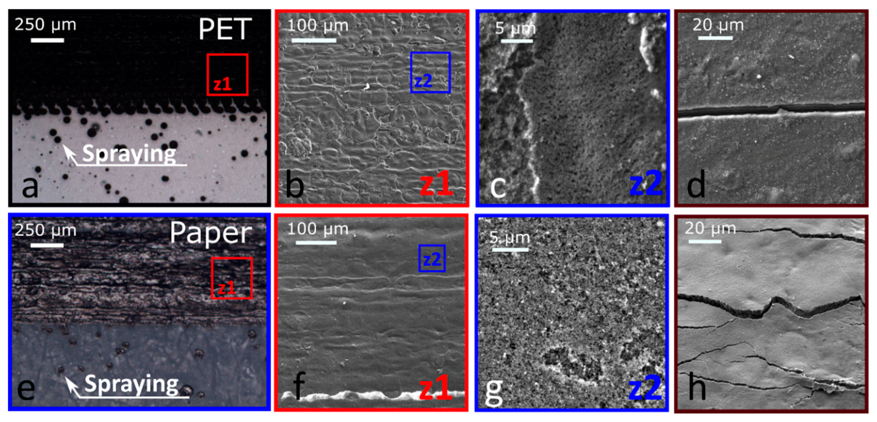
Abstract
1. Introduction
2. Materials and Methods
2.1. Carbon Black Based Ink
2.2. Egg White Based Ink
2.3. Printer and Substrates Description
2.4. Characterisation
3. Results
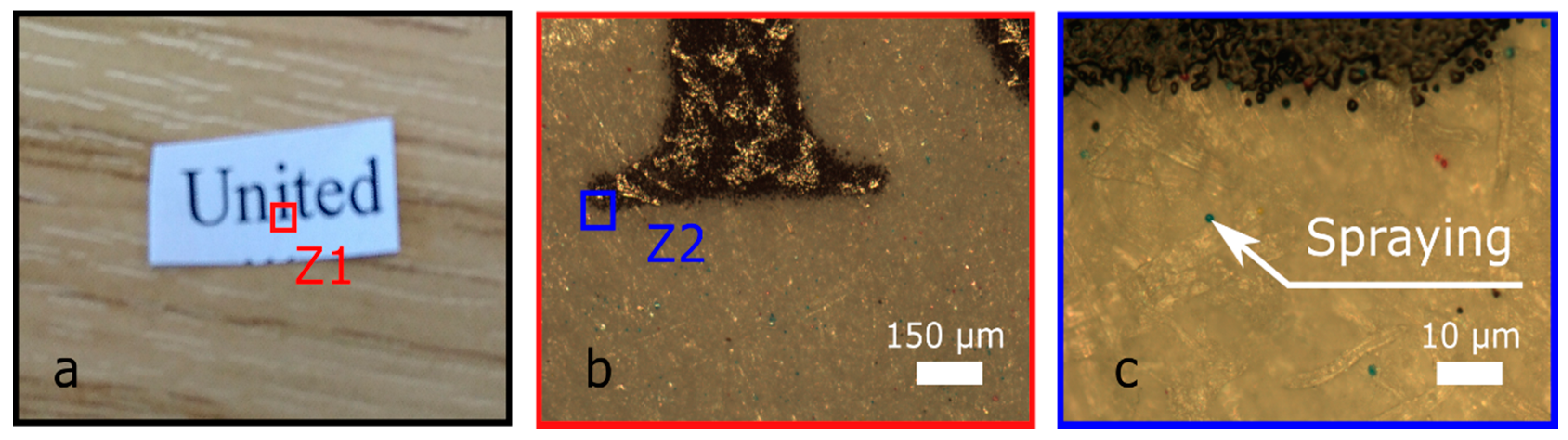
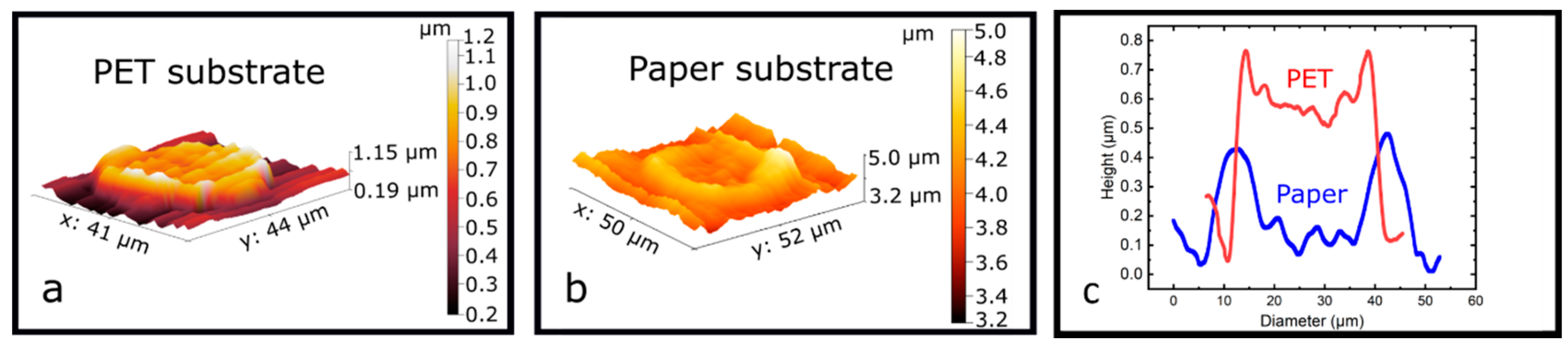
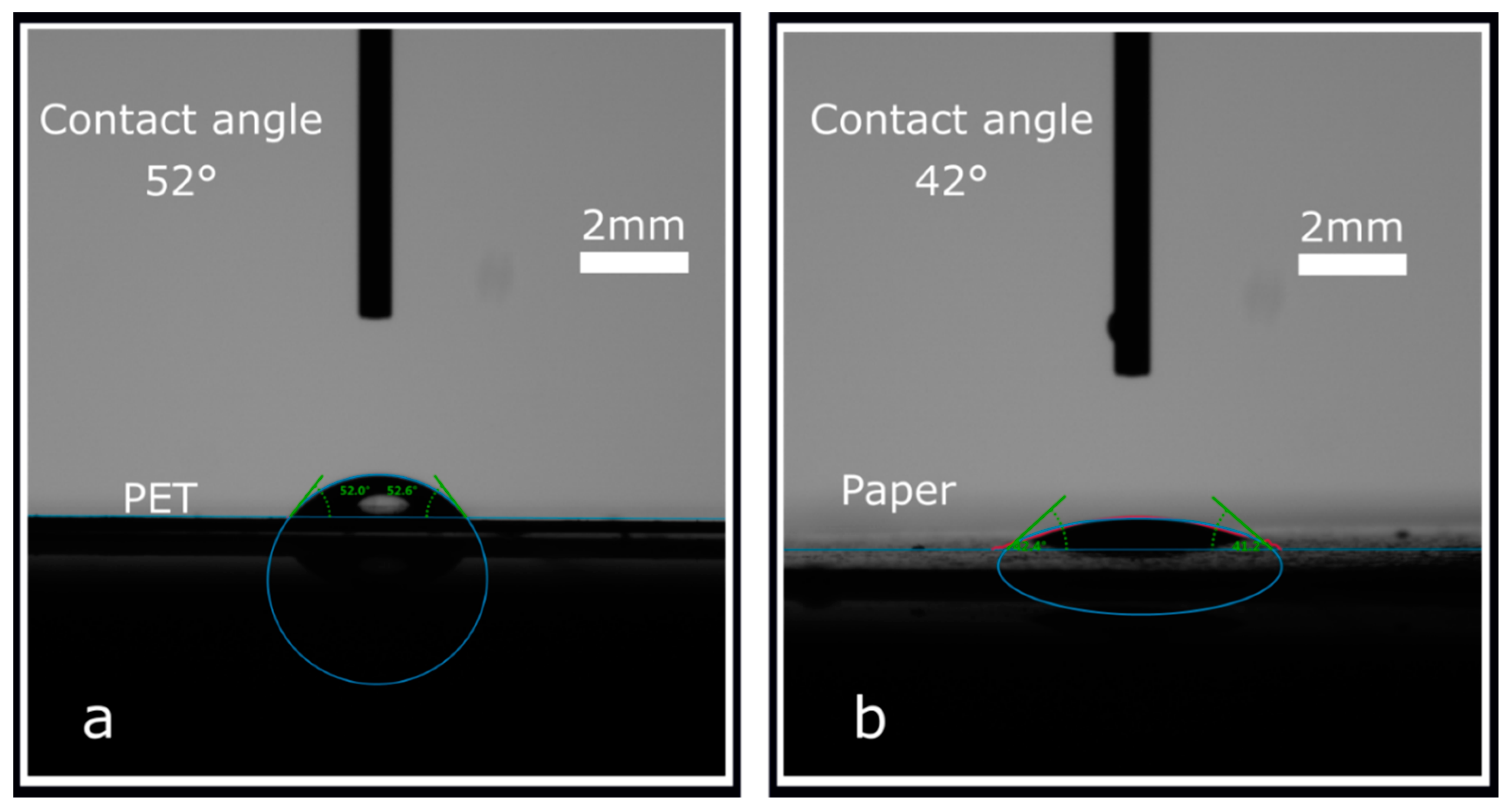
3.1. Ink Processing and Patterns Accuracy
3.2. Passive Device and Circuits
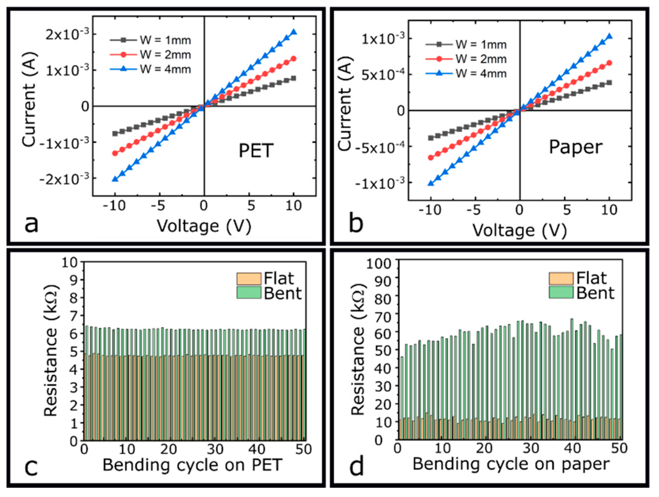
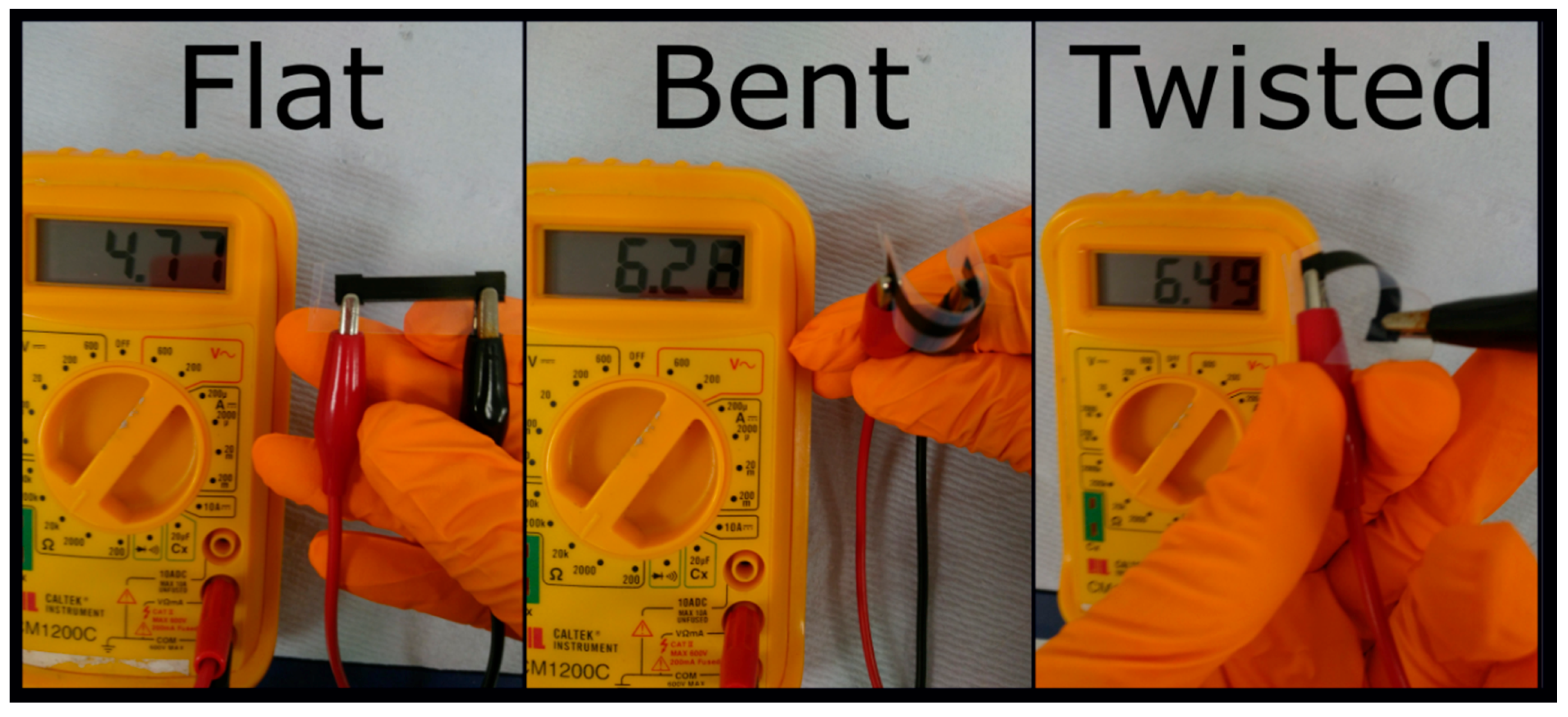
3.2.1. Resistors
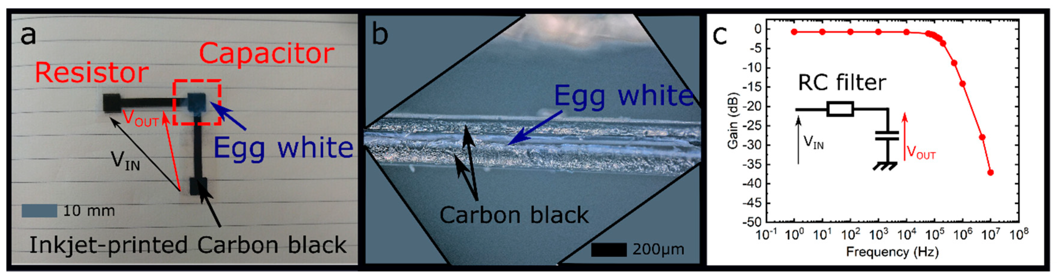
3.2.2. RC Filters
4. Conclusions
Author Contributions
Funding
Acknowledgments
Conflicts of Interest
Appendix A


References
- Prince, J.D. 3D printing: An industrial revolution. J. Electron. Resour. Med. Libr. 2014, 11, 39–45. [Google Scholar] [CrossRef]
- Huang, S.H.; Liu, P.; Mokasdar, A.; Hou, L. Additive manufacturing and its societal impact: A literature review. Int. J. Adv. Manuf. Technol. 2013, 67, 1191–1203. [Google Scholar] [CrossRef]
- Huang, Y.; Leu, M.C.; Mazumder, J.; Donmez, A. Additive manufacturing: Current state, future potential, gaps and needs, and recommendations. J. Manuf. Sci. Eng. 2015, 137, 014001. [Google Scholar] [CrossRef]
- Richardson, M.; Haylock, B. Designer/maker: The rise of additive manufacturing, domestic-scale production and the possible implications for the automotive industry. Comput.-Aided Des. Appl. PACE 2012, 2, 33–48. [Google Scholar] [CrossRef]
- Wilczynski, V. Academic Maker Spaces and Engineering Design; American Society for Engineering Education: Washington, DC, USA, 2015; Volume 26, p. 1. [Google Scholar]
- Browder, R.E.; Aldrich, H.E.; Bradley, S.W. The emergence of the maker movement: Implications for entrepreneurship research. J. Bus. Ventur. 2019. [Google Scholar] [CrossRef]
- Troxler, P. Fabrication laboratories (fab labs). In The Decentralized and Networked Future of Value Creation; Springer: Berlin/Heidelberg, Germany, 2016; pp. 109–127. [Google Scholar]
- Cressey, D. The DIY electronics transforming research. Nat. News 2017, 544, 125. [Google Scholar] [CrossRef] [PubMed]
- Le Borgne, B.; Jacques, E.; Harnois, M. The Use of a Water Soluble Flexible Substrate to Embed Electronics in Additively Manufactured Objects: From Tattoo to Water Transfer Printed Electronics. Micromachines 2018, 9, 474. [Google Scholar] [CrossRef]
- Street, R.A.; Ng, T.; Schwartz, D.E.; Whiting, G.L.; Lu, J.; Bringans, R.; Veres, J. From printed transistors to printed smart systems. Proc. IEEE 2015, 103, 607–618. [Google Scholar] [CrossRef]
- Fukuda, K.; Takeda, Y.; Yoshimura, Y.; Shiwaku, R.; Tran, L.T.; Sekine, T.; Mizukami, M.; Kumaki, D.; Tokito, S. Fully-printed high-performance organic thin-film transistors and circuitry on one-micron-thick polymer films. Nat. Commun. 2014, 5, 4147. [Google Scholar] [CrossRef]
- Cui, Z. Printed Electronics: Materials, Technologies and Applications; John Wiley & Sons: Hoboken, NJ, USA, 2016. [Google Scholar]
- Robin, M.; Kuai, W.; Amela-Cortes, M.; Cordier, S.; Molard, Y.; Mohammed-Brahim, T.; Jacques, E.; Harnois, M. Epoxy based ink as versatile material for inkjet-printed devices. ACS Appl. Mater. Interfaces 2015, 7, 21975–21984. [Google Scholar] [CrossRef]
- Shen, W.; Zhang, X.; Huang, Q.; Xu, Q.; Song, W. Preparation of solid silver nanoparticles for inkjet printed flexible electronics with high conductivity. Nanoscale 2014, 6, 1622–1628. [Google Scholar] [CrossRef] [PubMed]
- Tao, Z.; Le Borgne, B.; Mohammed-Brahim, T.; Jacques, E.; Harnois, M. Spreading and drying impact on printed pattern accuracy due to phase separation of a colloidal ink. Colloid Polym. Sci. 2018, 296, 1749–1758. [Google Scholar] [CrossRef]
- Soltman, D.; Subramanian, V. Inkjet-printed line morphologies and temperature control of the coffee ring effect. Langmuir 2008, 24, 2224–2231. [Google Scholar] [CrossRef] [PubMed]
- Derby, B. Inkjet printing of functional and structural materials: Fluid property requirements, feature stability, and resolution. Annu. Rev. Mater. Res. 2010, 40, 395–414. [Google Scholar] [CrossRef]
- Ko, S.H.; Pan, H.; Grigoropoulos, C.P.; Luscombe, C.K.; Fréchet, J.M.; Poulikakos, D. All-inkjet-printed flexible electronics fabrication on a polymer substrate by low-temperature high-resolution selective laser sintering of metal nanoparticles. Nanotechnology 2007, 18, 345202. [Google Scholar] [CrossRef]
- Calvert, P. Inkjet printing for materials and devices. Chem. Mater. 2001, 13, 3299–3305. [Google Scholar] [CrossRef]
- De Gans, B.-J.; Kazancioglu, E.; Meyer, W.; Schubert, U.S. Ink-jet printing polymers and polymer libraries using micropipettes. Macromol. Rapid Commun. 2004, 25, 292–296. [Google Scholar] [CrossRef]
- Jang, D.; Kim, D.; Moon, J. Influence of fluid physical properties on ink-jet printability. Langmuir 2009, 25, 2629–2635. [Google Scholar] [CrossRef]
- Deegan, R.D.; Bakajin, O.; Dupont, T.F.; Huber, G.; Nagel, S.R.; Witten, T.A. Capillary flow as the cause of ring stains from dried liquid drops. Nature 1997, 389, 827. [Google Scholar] [CrossRef]
- Peng, X.; Yuan, J.; Shen, S.; Gao, M.; Chesman, A.S.; Yin, H.; Cheng, J.; Zhang, Q.; Angmo, D. Perovskite and organic solar cells fabricated by inkjet printing: Progress and prospects. Adv. Funct. Mater. 2017, 27, 1703704. [Google Scholar] [CrossRef]
- Van der Vaart, N.; Lifka, H.; Budzelaar, F.; Rubingh, J.; Hoppenbrouwers, J.; Dijksman, J.; Verbeek, R.; Van Woudenberg, R.; Vossen, F.; Hiddink, M.; et al. Towards large-area full-color active-matrix printed polymer OLED television. J. Soc. Inf. Disp. 2005, 13, 9–16. [Google Scholar] [CrossRef]
- Moon, S.J.; Robin, M.; Wenlin, K.; Yann, M.; Bae, B.S.; Mohammed-Brahim, T.; Jacques, E.; Harnois, M. Morphological impact of insulator on inkjet-printed transistor. Flex. Print. Electron. 2017, 2, 035008. [Google Scholar] [CrossRef]
- Fukuda, K.; Sekine, T.; Kumaki, D.; Tokito, S. Profile control of inkjet printed silver electrodes and their application to organic transistors. ACS Appl. Mater. Interfaces 2013, 5, 3916–3920. [Google Scholar] [CrossRef] [PubMed]
- Goosey, M. End-of-life electronics legislation—An industry perspective. Circuit World 2004, 30, 41–45. [Google Scholar] [CrossRef]
- Irimia-Vladu, M.; Sariciftci, N.S.; Bauer, S. Exotic materials for bio-organic electronics. J. Mater. Chem. 2011, 21, 1350–1361. [Google Scholar] [CrossRef]
- Stavrinidou, E.; Gabrielsson, R.; Gomez, E.; Crispin, X.; Nilsson, O.; Simon, D.T.; Berggren, M. Electronic plants. Sci. Adv. 2015, 1, e1501136. [Google Scholar] [CrossRef] [PubMed]
- Tao, Z.; Mohammed-Brahim, T.; Lei, W.; Harnois, M.; Jacques, E. Impact of the post-thermal annealing on OFETs using printed contacts, printed organic gate insulator and evaporated C60 active layer. Solid-State Electron. 2018, 150, 51–59. [Google Scholar] [CrossRef]
- Kalb, W.L.; Mathis, T.; Haas, S.; Stassen, A.F.; Batlogg, B. Organic small molecule field-effect transistors with CytopTM gate dielectric: Eliminating gate bias stress effects. Appl. Phys. Lett. 2007, 90, 092104. [Google Scholar] [CrossRef]
- Lu, Y.; Fujii, M. Dielectric analysis of hen egg white with denaturation and in cool storage. Int. J. Food Sci. Technol. 1998, 33, 393–399. [Google Scholar] [CrossRef]
- Irimia-Vladu, M. “Green” electronics: Biodegradable and biocompatible materials and devices for sustainable future. Chem. Soc. Rev. 2014, 43, 588–610. [Google Scholar] [CrossRef] [PubMed]
- Bibi, F.; Villain, M.; Guillaume, C.; Sorli, B.; Gontard, N. A review: Origins of the dielectric properties of proteins and potential development as bio-sensors. Sensors 2016, 16, 1232. [Google Scholar] [CrossRef] [PubMed]
- Wu, G.; Feng, P.; Wan, X.; Zhu, L.; Shi, Y.; Wan, Q. Artificial synaptic devices based on natural chicken albumen coupled electric-double-layer transistors. Sci. Rep. 2016, 6, 23578. [Google Scholar] [CrossRef] [PubMed]
- Zhou, Y.; Fuentes-Hernandez, C.; Khan, T.M.; Liu, J.-C.; Hsu, J.; Shim, J.W.; Dindar, A.; Youngblood, J.P.; Moon, R.J.; Kippelen, B. Recyclable organic solar cells on cellulose nanocrystal substrates. Sci. Rep. 2013, 3, 1536. [Google Scholar] [CrossRef] [PubMed]
- Glowacki, E.D.; Leonat, L.; Voss, G.; Bodea, M.; Bozkurt, Z.; Irimia-Vladu, M.; Bauer, S.; Sariciftci, N.S. Natural and nature-inspired semiconductors for organic electronics. In Organic Semiconductors in Sensors and Bioelectronics IV; International Society for Optics and Photonics, SPIE Digital Library: Sergy-Pontoise, France, 2011; Volume 8118, p. 81180M. [Google Scholar]
- Chiappini, C.; Liu, X.; Fakhoury, J.R.; Ferrari, M. Biodegradable porous silicon barcode nanowires with defined geometry. Adv. Funct. Mater. 2010, 20, 2231–2239. [Google Scholar] [CrossRef] [PubMed]
- Petritz, A.; Wolfberger, A.; Fian, A.; Irimia-Vladu, M.; Haase, A.; Gold, H.; Rothländer, T.; Griesser, T.; Stadlober, B. Cellulose as biodegradable high-k dielectric layer in organic complementary inverters. Appl. Phys. Lett. 2013, 103, 191_1. [Google Scholar] [CrossRef]
- Capelli, R.; Amsden, J.J.; Generali, G.; Toffanin, S.; Benfenati, V.; Muccini, M.; Kaplan, D.L.; Omenetto, F.G.; Zamboni, R. Integration of silk protein in organic and light-emitting transistors. Org. Electron. 2011, 12, 1146–1151. [Google Scholar] [CrossRef] [PubMed]
- Le Borgne, B.; De Sagazan, O.; Crand, S.; Jacques, E.; Harnois, M. Conformal Electronics Wrapped Around Daily Life Objects Using an Original Method: Water Transfer Printing. ACS Appl. Mater. Interfaces 2017, 9, 29424–29429. [Google Scholar] [CrossRef]
- Le Borgne, B.; Liu, S.; Morvan, X.; Crand, S.; Sporea, R.A.; Lu, N.; Harnois, M. Water Transfer Printing Enhanced by Water-Induced Pattern Expansion: Toward Large-Area 3D Electronics. Adv. Mater. Technol. 2019. [Google Scholar] [CrossRef]
- Fukuhira, Y.; Kitazono, E.; Hayashi, T.; Kaneko, H.; Tanaka, M.; Shimomura, M.; Sumi, Y. Biodegradable honeycomb-patterned film composed of poly (lactic acid) and dioleoylphosphatidylethanolamine. Biomaterials 2006, 27, 1797–1802. [Google Scholar] [CrossRef]
- Martins, R.F.; Ahnood, A.; Correia, N.; Pereira, L.M.; Barros, R.; Barquinha, P.M.; Costa, R.; Ferreira, I.M.; Nathan, A.; Fortunato, E.E. Recyclable, flexible, low-power oxide electronics. Adv. Funct. Mater. 2013, 23, 2153–2161. [Google Scholar] [CrossRef]
- Muskovich, M.; Bettinger, C.J. Biomaterials-based electronics: Polymers and interfaces for biology and medicine. Adv. Healthc. Mater. 2012, 1, 248–266. [Google Scholar] [CrossRef] [PubMed]
- King, S.G.; Castaldelli, E.; McCaffterty, L.; Silva, S.R.P.; Stolojan, V. Micro-Centrifugal Technique for Improved Assessment and Optimization of Nanomaterial Dispersions: The Case for Carbon Nanotubes. ACS Appl. Nano Mater. 2018, 1, 6217–6225. [Google Scholar] [CrossRef]
- Limousy, L.; Jeguirim, M.; Labbe, S.; Balay, F.; Fossard, E. Performance and emissions characteristics of compressed spent coffee ground/wood chip logs in a residential stove. Energy Sustain. Dev. 2015, 28, 52–59. [Google Scholar] [CrossRef]
- Bach, C.; Dauchy, X.; Etienne, S. Characterization of poly (ethylene terephthalate) used in commercial bottled water. In IOP Conference Series: Materials Science and Engineering; IOP Publishing: Bristol, UK, 2009; Volume 5, p. 012005. [Google Scholar]
- Ajji, A.; Chapleau, N. Structure and properties of impact modified polyethylene terephthalate. J. Mater. Sci. 2002, 37, 3893–3901. [Google Scholar] [CrossRef]
- McGuigan, A.; Briggs, G.; Burlakov, V.; Yanaka, M.; Tsukahara, Y. An elastic–plastic shear lag model for fracture of layered coatings. Thin Solid Films 2003, 424, 219–223. [Google Scholar] [CrossRef]


© 2019 by the authors. Licensee MDPI, Basel, Switzerland. This article is an open access article distributed under the terms and conditions of the Creative Commons Attribution (CC BY) license (http://creativecommons.org/licenses/by/4.0/).
Share and Cite
Le Borgne, B.; Chung, B.-Y.; Tas, M.O.; King, S.G.; Harnois, M.; Sporea, R.A. Eco-Friendly Materials for Daily-Life Inexpensive Printed Passive Devices: Towards “Do-It-Yourself” Electronics. Electronics 2019, 8, 699. https://doi.org/10.3390/electronics8060699
Le Borgne B, Chung B-Y, Tas MO, King SG, Harnois M, Sporea RA. Eco-Friendly Materials for Daily-Life Inexpensive Printed Passive Devices: Towards “Do-It-Yourself” Electronics. Electronics. 2019; 8(6):699. https://doi.org/10.3390/electronics8060699
Chicago/Turabian StyleLe Borgne, Brice, Bo-Yan Chung, Mehmet O. Tas, Simon G. King, Maxime Harnois, and Radu A. Sporea. 2019. "Eco-Friendly Materials for Daily-Life Inexpensive Printed Passive Devices: Towards “Do-It-Yourself” Electronics" Electronics 8, no. 6: 699. https://doi.org/10.3390/electronics8060699
APA StyleLe Borgne, B., Chung, B.-Y., Tas, M. O., King, S. G., Harnois, M., & Sporea, R. A. (2019). Eco-Friendly Materials for Daily-Life Inexpensive Printed Passive Devices: Towards “Do-It-Yourself” Electronics. Electronics, 8(6), 699. https://doi.org/10.3390/electronics8060699