Abstract
The need for the fabrication of a new generation of devices has developed with the next generation of ‘home’ engineers, which is resulting in an ever-increasing population interested in “do-it-yourself” electronics and the Internet of Things. However, this new trend should not be done at the expense of the environment. Almost all previous studies, related to the low-temperature processing of devices, fail to highlight the extent of the impact that the synthesis of these technologies have on both the environment and human health. In addition, the substrates typically used, are also often associated with major drawbacks such as a lack of biodegradability. In this paper, we fabricate a simple RC filter using various domestically available printing techniques, utilising readily available materials such as: carbon soots (carbon black) as an electric conductor, and egg white (albumen) as a dielectric. These devices have been fabricated on both polyethylene terephthalate (PET) and paper, which demonstrated the same performances on both substrates and revealed that recyclable substrates can be used without compromise to the devices’ performance. The filter was found to exhibit a cut-off frequency of 170 kHz, which made it suitable for high-frequency reception applications.
1. Introduction
Additive manufacturing technologies have gained a growing interest in the past decade [1,2,3]. Industry has understood the potential of additive manufacturing technologies pushing them to reach the ultimate goal of the fabrication of low cost, mass market products at high throughput. Currently, printing technologies are not restricted to mass manufacturing because modern low-cost domestic printers allow domestic users to take advantage of these versatile technologies. Users appear to utilise these technologies for a range of applications, including the fabrication or the reparation of daily life objects, their hobbies, or even educational purposes [4,5,6]. 3D printing technology is the most famous example and fused deposition modelling (FDM) based printers can be found everywhere [7]. Consequently, it can be anticipated that the “do it yourself” (DIY) movement will continue to promote printed electronics technology, as every DIY user essentially already has their own commercial Drop on Demand (DoD) printer at home [8]. Furthermore, a recent study has already suggested that 3D printing (such as FDM) can be combined with printed electronics to fabricate 3D Electronics [9].
However, to date, printing technologies have been mainly investigated by researchers and industry aiming to fabricate complex devices using high tech equipment [10,11,12]. These investigations have led to fascinating innovations involving a wide span of skills in the field of the ink design [13,14], the analysis of the ink, and the substrate interactions [13,15,16] as well as the pattern resolution and accuracy improvement [17,18]. These studies should be made considering the environmental impact and proposing alternatives to non-sustainable materials.
Ink design is complex because its rheological properties have a strong impact on the jetting behavior. Special attention has to be paid to obtain reliable ink jetting, mainly due to nozzle clogging, long lived filament, satellite droplet, etc. Consequently, an optimum ink formulation avoiding the previously mentioned drawbacks needs strong expertise to choose an appropriate low boiling point solvent, low molecular weight ink, nanoparticle size, etc. [19,20]. Jetting parameters (firing voltage, firing time, etc.) that are only customisable using a high-tech printer are also crucial to print high quality patterns. These factors must be considered to ensure ideal parameters are used in printers that lack customisation [13]. For instance, it has been shown that unstable satellite droplets do not fall down through the same axis as the main droplet and play a crucial role on the pattern definition. Pattern formation on the substrate is another key step to evaluate the printing process, where the pattern is often formed by solid material dispersed in liquid adhering to the substrate [21]. A droplet deposited on the surface is submitted to a drying mechanism, which leads to nonuniform film formation, caused, for instance, by the “coffee stain effect” or driven by an undesirable spreading phenomena [22].
A careful optimisation of all of these experimental parameters in combination with new materials development are mandatory to fabricate complex devices such as printed solar cells [23], organic light emitted diodes (OLED) [24], organic field effect transistors (OFET) [25], and circuits [11]. For instance, when printing devices such as an OFET, if the contact electrodes such as gate or drain and source show a non-uniform profile, electrical characteristics will be negatively impacted [25,26]. Consequently, it is not usually possible for DIY users to fabricate these complex devices, which means they will be restricted to industry and professional researchers. However, our work highlights that printing technologies can be used by those in the DIY movement to fabricate simple strain sensors and passive circuits using a commercial desktop printer. Since literature is lacking such examples, it also shows that eco-friendly materials can be used to achieve such devices.
If printing electronics are to become common practice such as for 3D printing, it should not be done at the detriment to the environment [27]. Recently, various groups have developed electronic devices using daily-life materials, such as albumen (egg white), fish gelatine [28], or flowers [29] as either insulators, mixers, or even microfluidic channels, respectively. These studies present the combined interests in dealing with cheap and almost non-transformed materials, which could lead to new forms of innovation for large public users. If solution-based insulators such as SU8-photoresists [30] and Cytop [31], for example, are available off the shelf, the use of proteins such as the ones found within the albumen is much more sustainable [32]. Moreover, albumen has a dielectric constant of ε = 5.2 [33], which is good enough for numerous electronic applications, including for sensors or passivation layers, where high speed components are not required. Bibi et al. showed that proteins exhibit interesting dielectric permittivity and loss factors, which are suitable with standard electronic requirements [34]. The albumen has been reported previously as dielectrically compatible with the fabrication of transistors [35].
The choice of the substrate is also something that is rarely discussed in most studies. However, the most commonly used substrates in the field of printed/flexible electronics are polyethylene terephthalate (PET), polyethylene naphthalate (PEN), polycarbonate (PC), and polyimide (PI), even though it is well known that these type of plastics may take anything from 30 to more than 400 years to decompose, which presents a significant environmental issue [36].
So far, it is clear that fully bio-sourced and non-modified materials cannot compete with the performance of engineered materials, which have been developed over several decades. However, environmental sustainability needs to render it important to start using these materials for electronic use. Furthermore, it is particularly important since most of the materials are already readily available. Some studies have shown that bio-sourced, biocompatible, or non-toxic materials for electronics such as semiconductors [37], conductors [33,38], dielectrics [39,40] substrates [41,42,43,44], and adhesives [45] have promising performance as greener alternatives.
In the work reported here, we demonstrate how to fabricate DIY and eco-friendly electronic devices. In this case, we create an RC filter, using daily-life products and a cheap domestic household desktop inkjet printer. The robustness of the technique is demonstrated by repeating the steps numerous times over, which leads to a distribution of the measured performances of the devices of less than 10%, which is close to the conventional performances presented in the literature with other printed flexible electronics.
2. Materials and Methods
2.1. Carbon Black Based Ink
The carbon black (CB) used in this study was supplied by Columbian Chemicals (Hanover, Germany) as the product ‘Raven® P’, which had a particle size of 22 nm. The aqueous based ink was blended by dispersing 10% w/w CB with 5% w/w of surfactant sodium dodecyl sulfate (SDS). The resulting solution was subject to ultrasonication using a Cole-Palmer 750 W horn-probe sonicator while being cooled in an ice bath. The homogenisation process was conducted at 40% sonication power for a total of 30 min, which was pulsed in durations of 1 s on and 1 s off. This was previously found to have the optimum parameters [45]. It should be noted that, the production of soots during everyday life is an unavoidable issue. Fortunately, solutions also exist to reduce it and to produce it in a more sustainable way [46,47]. However, in contrast to most other currently available conductive inks, which typically use hazardous solvents such as Diethylene glycol (DEG) and Diphenyl–2,4,6–trimethylbenzoyl phosphine oxide (TPO), no solvents other than deionised water was used to formulate the inks used in this study, which ensures our inks are both non-hazardous to home users and environmentally-friendly.
Once fully prepared, the ink was referred to as “CB ink.” The previous parameters were fine-tuned in order to facilitate the inks jetability. The final viscosity of the ink was measured using a Brookfield DVII+ Pro viscometer and found at 4.69 cP.
2.2. Egg White Based Ink
The egg white (albumen) was prepared by simply separating the albumen from the yolk. Since there is no need to inkjet-print this material, no additional post processing was applied. The viscosity was found at 20.1 cP.
2.3. Printer and Substrates Description
The printer used in this study was an Epson Stylus C88+. It was set-up with refillable empty compatible ink cartridges for Epson T0711 (Auto Reset Chips) purchased from eBay. The cartridges were refilled as necessary using a needle and syringe. Despite the apparent jetability of the ink, clogging phenomena of the print head was frequently observed. Consequently, the printhead was frequently cleaned using a Metalon™ Aqueous Vehicle solution (purchased from Novacentrix, Austin, TX, USA).
The screen-printing method was performed by simply using a piece of thin cardboard (10 cm × 10 cm × 150 µm) with an opening realised using a scalpel. The dimension of the square opening was the size of the desired insulating area (10 mm²).
The plastic (PET-based) substrates were purchased from Novacentrix (Novele™ Pack, 8.5” × 11” × 140 µm). The paper carrier substrates were purchased at Canson (Infinity, Baryta Photographique, 310 g/m², 21 × 29.7 cm × 305 µm). The primary reason for the use of photo paper, over other more commonly available papers, was due to its wetting resistance, which reduced its likelihood of becoming too saturated during the screen printing of the egg white.
2.4. Characterisation
Optical pictures were taken using a LEICA 2500P microscope equipped with a digital camera (LEICA DFC420, Wetzlar, Germany ). Surface morphologies of the inkjet-printed inks were analysed using a TESCAN MIRA II scanning electron microscope (SEM). Electrical I (V) characteristics were obtained using a Keysight B1500A semiconductor analyser. The RC filter behaviour was measured using a Keysight DSOX2002A digital oscilloscope (bandpass 70 MHz) and a Thurbly Thandar Instrument TG1010 programmable function generator (maximum frequency 10 MHz). Bending experiments were performed using a rigid rod (bending radius equals = 4 mm). To test the printed resistors, they were first affixed onto rigid rods before being measured (I (V) measurements). For the second stage of testing, the resistors were removed from the rods and then flattened before further measurements. These two stages were repeated 50 times to measure the device durability. For improved electrical contact during the bending stage, copper tape was placed on the electrodes. A cycle consists in bending the devices until it reaches the desired bending radius before measuring the resistance value. Figure A5 shows the resistor’s behavior in a flat, bent, and even twisted configuration.
The capacitance of the CB and albumen-based capacitor was measured using a TENMA 72-7770 (Premier Farnell, Leeds, UK) capacitance-meter.
The contact angles were measured three times on each of the substrates and the presented value is averaged over numerous repeat measurements. These values were obtained using a Krüss DSA25B apparatus equipped with a camera TAMRON 1:39 (IDS, 75 mm, Ø25.5 mm) and coupled with the Krüss Advance software.
Droplet profiles and mapping were performed using a Dektak XT profilometer. The scan used a 12.5 µm stylus and the applied force was 2 mg. The apparatus uses the Vision 64 software. The 3D mapping were plotted using Gwyddion software (Version 2.53).
3. Results
3.1. Ink Processing and Patterns Accuracy
The CB ink was prepared and printed as previously outlined. Since domestic desktop printers were used for this investigation, no experimental parameters were customised or monitored. The resolution of the printer was kept constant for all the experiments and fixed to 300 dpi. Patterns were designed using an open source drawing software (Inkscape, version 0.92.4), which allows for an easy design stage mandatory for DIY electronics. As shown in Figure 1, the CB ink was printed onto PET and paper-based substrates. The PET substrate is one of the most frequently used in the field of printed electronics. PET substrates are, indeed, compatible with a wide range of applications because of its low cost, thermal stability, spin ability, and moisture resistance [48,49]. However, in order to respect the WEEE (Waste Electrical and Electronic Equipment) standard, waste management must be taken into consideration to contribute to the circular economy. The devices outlined in this work will take into consideration such challenging issues. This is why paper-based substrates have also been studied as an alternative eco-friendly substrate.
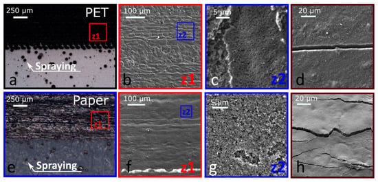
Figure 1.
SEM pictures of a 2 mm-wide CB line printed on PET (a–d) and paper (e–h). (a) Imaging of the PET substrate, which highlights the spraying phenomenon inherent to desktop printers. (b) Magnification showing that the substrate is fully covered by the ink (c,d) some cracks appear but do not prevent conduction. (e) Imaging of the paper substrate. (f) Magnification showing that the substrate is fully covered by the ink. The paper is soaked by the ink (g,h) appearance of cracks at the surface of the CB ink printed line.
Figure 1a,e show optical pictures of the patterns’ side along the printing direction for PET and Paper substrates, respectively. For both experiments, isolated droplets were observed outside the vicinity of the printed patterns, which highlighted unwanted spraying during the printing. Such undesirable satellites droplets are detrimental for the accuracy and resolution of the printed pattern. When a desktop printer is used, no fiducial camera is available to watch the droplets jetting behaviours, which makes analysing this behaviour challenging. Moreover, because this investigation uses a standard domestic printer, users cannot fix the jetting parameters to respect any optimum jetting criteria [13]. Consequently, the designed pattern width has to be large enough to avoid any electrical breaks (open circuits) introduced during printing and the distance between two adjacent patterns has to be increased to a minimum distance in order to avoid unwanted interconnects (short circuits).
In similarity to metallic-based inks (e.g., containing silver or copper nanoparticles), a core-shell structure has been grafted around the CB nanoparticles in the form of a suitable surfactant micellar layer. However, in contrast, no additional post baking stage (i.e., sintering stage to destroy the core shell) of the patterns was required to provide conductive patterns. This was because our CB ink used a well-known widely available surfactant, which commonly found in domestic soap: SDS, which is intrinsically ionically conductive. All that was required for the printing of our CB ink was a fast-drying time of approximately 1 min, which allows the aqueous-based solvent to fully evaporate. This was all that was necessary to obtain an ohmic behaviour as described in the next section. Moreover, optical observations in the Appendix A Figure A1 highlight that, even if the ink is not sintered like alternative metal nanoparticle based inks, it does not re-dissolve when immersed in the original solvent, which is water, in this case.
Figure 1a,e demonstrate a close-up of a printed line (for use as a resistor) on both substrates used in this investigation. It can be observed that the desktop printer introduces a lot of spraying. However, the observed spraying phenomenon is no worse than what was seen during the printing of classical coloured pigment inks, as shown in Appendix AFigure A2. It is important to point out that the working behaviour of the printed resistor was not altered or hindered by the spraying.
The stray sprayed droplets were scanned using a profilometer to highlight the drying process of the ink on the two substrates (see Appendix A Figure A3). It was found that the droplets spread further across the substrate surface when using paper than with PET. We found this result is mainly due to the increased ink absorption by the paper, as it is well known that fibrous materials absorb more liquid, spreading ink through capillary action. Furthermore, this observation is in good agreement with the measured water contact angle (see in Figure A4), which is higher in the case of PET (52°) than the paper-based substrate (42°). Consequently, the unwanted spreading effect during the drying of CB ink when on paper substrates led to the previously mentioned coffee stain effect.
Despite the spraying, the coffee stain effect and the lack of printing parameter controllability of such domestic printers, functional devices can easily be printed, including by a DIY user. It can clearly be observed, as shown in Figure 1b,c,f,g that the printed patterns are completely filled and do not present holes or missing material. However, as shown in Figure 1d,h, when the substrates are bent more than 5 mm (i.e., bending radius), cracks are observed in the printed CB film. It was noticed that the morphology and the density of cracks typically tended to be linear in direction and less densely packed for the prints on a PET substrate. Whereas, in comparison, cracks observed on paper-based substrates were randomly oriented and more densely packed. This could be due to the elasticity of the paper-based substrate, as already observed in the literature [50].
3.2. Passive Device and Circuits
3.2.1. Resistors
To print various resistors, conductive carbon ribbons were printed with varying geometries (L = 2 cm and W = 1 mm, 2 mm, and 4 mm). The current versus voltage (I (V)) curves in Figure 2a,b highlight that patterns printed using CB-based ink show ohmic behaviour on both PET and paper substrates. Since the CB inks typically print resistive devices, it is important to note that CB inks would be unsuitable when used in application where efficient conductive electrodes are mandatory, such as printed transistors (i.e., it will dramatically lead to a high access resistance values in comparison to alternative silver-based ink, for instance) [25]. However, many applications can benefit from CB-based inks, especially those dealing with variable resistances, such as a strain sensor. As shown in the Figure 2c,d, the resistance of the printed resistors varied from 11.7 kΩ (±24.7%) to 59 kΩ (±17.0%) when it was kept flat to when it was bent with a radius of curvature of 4 mm. The behaviour of the strain sensors did not show significant evolution during the 50 bending cycles or when it was twisted, as shown in the Appendix A Figure A5.
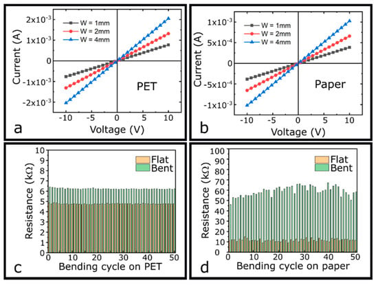
Figure 2.
Electrical behaviour of the CB ink printed resistors under strain. Current versus voltage plots on (a) plastic and (b) paper substrates. Measured resistances during 50 bending cycles of the inkjet-printed CB line (W = 4 mm) in flat and bent positions for the (c) plastic and (d) paper substrates. Bending radius was kept constant at 4 mm.
3.2.2. RC Filters
Multi-layered eco-friendly devices were printed onto a PET substrate using CB-based ink as conductors and egg white based ink as insulators. The RC filters were made in three technological stages. The first stage consisted of printing the resistor (L = 2 cm, W = 4 mm) and the bottom electrode of the capacitor (area = 5 mm²).
The egg white was not printed using DoD printing technology because its rheological properties do not meet the printing requirements. This was because the viscosity (20.9 cp) of the protein is too high, which will cause the occurrence of print nozzles clogging. In these cases, screen printing technology is more suitable.
As such, the egg white is then manually screen printed using a stencil and a doctor’s blade, as shown operating the equipment in Figure A6. The opening in the stencil is square-shaped (area = 10 mm²) and is purposely wider than the capacitor’s electrode to avoid any risks of a short-circuit (between the electrodes). The substrate is then baked at 60 °C, for a duration of 5 min in order to dry the device.
Lastly, the top electrode was printed (area = 5 mm²). The substrate was then baked a second time at 60 °C for another 5-min duration. Figure 3a,b show optical observations of the devices as top-view and cross section, respectively. The image Figure 3b highlights that the thin film of egg white (150 µm thick) is continuous and avoids any short circuit, which would leak current.

Figure 3.
RC filter. (a) Optical image of the device composed of a resistor and a capacitor in series. The resistor and the capacitor’s electrodes are made of a printed carbon. The egg white, used as insulator, is screen printed. (b) An optical microscope image of the capacitor stack, showing the PET substrate, the CB, and the insulating layers. (c) A schematic diagram of the RC filter and the obtained magnitude Bode diagram.
The device’s frequency response was then electrically evaluated. The input voltage (see VIN in Figure 3a,c) is fixed at 2V (peak-to-peak) and its frequency varied from 1 Hz to 10 MHz. The output voltage was monitored (see VOUT in Figure 3a,c) during the frequency sweep. Figure 3c shows the obtained Bode plot gain response. The cut-off frequency (at −3 dB) of the device was found to be 170 kHz. The capacitance of the printed device was measured to be around 0.35 nF, whereas the resistance was measured to be 5 kΩ (see previous section). According to standard electronics, the cut-off frequency is calculated as: fc = 1/2 πRC where R is the resistance and C is the capacitance of the filter’s components. The expected cut-off frequency should be around 90 kHz. This means that we obtained a factor 2 difference between experimental and theoretical value. This is likely due to residual leakage in the capacitor and variation of the impedance in the filter. However, for such novel materials, these shifts are not surprising. For DIY domestic user applications, such a dispersion, should not be a major drawback since it is easy to fabricate numerous devices, which adapts, on demand, the resistance value.
4. Conclusions
Using readily available materials found in the average domestic home, aqueous-based environmentally-friendly carbon inks were fabricated and successfully inkjet printed on a standard, inexpensive, common domestic printer to fabricate a range of electronic devices, which all use a cost-effective and simple process applicable to DIY home users. Simple, easily customisable resistors were printed and demonstrated on both PET and paper substrates, where bending and twisting over numerous cycles saw zero degradation of their performance. By monitoring the resistance of one of these devices during bending, we also demonstrated a working strain gauge. By combining the inkjet printing of the same carbon ink with the screen printing of egg white onto a PET substrate, we successfully fabricated a low-cost low-pass filter, using inexpensive and green materials used in daily life. The realisation of such a filter demonstrates that, with these suitable materials, RC filters and eventually more complex devices such as transistors can be produced at home. These results from our investigation should encourage more investigations in this field of study. The use of greener materials can make electronics more sustainable and could also be a progression toward fully recyclable electronics, which is a major challenge that we should already address. Future developments to allow the inkjet printing of the egg white could easily be made with further solution processing. This would improve the consistency of device production with the techniques used. Efforts should also be pursued to develop libraries of working basic components such as resistors, capacitors, and transistors in order to propose off-the-shelf green “integrated” circuits, which can be simply looked up and fabricated.
Author Contributions
Conceptualization, B.L.B. Methodology, B.-Y.C., B.L.B. and M.H. Validation, B.-Y.C., M.O.T. and S.G.K. Formal analysis, B.L.B., S.G.K. and M.H. Writing—Review and editing, M.H., B.L.B. and S.G.K. Visualization, M.O.T. Supervision, B.L.B. Project administration, R.A.S. Funding acquisition, R.A.S.
Funding
The EPSRC: grant numbers EP/R028559/1 and EP/N006372/1 and the Surrey SATRO scheme funded this research.
Acknowledgments
Authors thank Inkyu Kwon for his help for the experimental work performed in this article. Authors also thank the Surrey SATRO scheme for the administrative support.
Conflicts of Interest
The authors declare no conflict of interest.
Appendix A
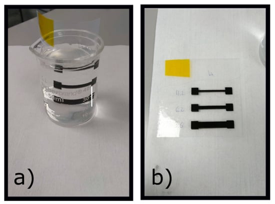
Figure A1.
Inkjet-printed carbon black lines showing their waterproof nature and good adhesion to the PET substrate. (a) Dipping into the water. No dissolution of the ink was observed and, (b) after 10 min in the water, the measured resistance were the same as before the immersion.
Figure A1.
Inkjet-printed carbon black lines showing their waterproof nature and good adhesion to the PET substrate. (a) Dipping into the water. No dissolution of the ink was observed and, (b) after 10 min in the water, the measured resistance were the same as before the immersion.
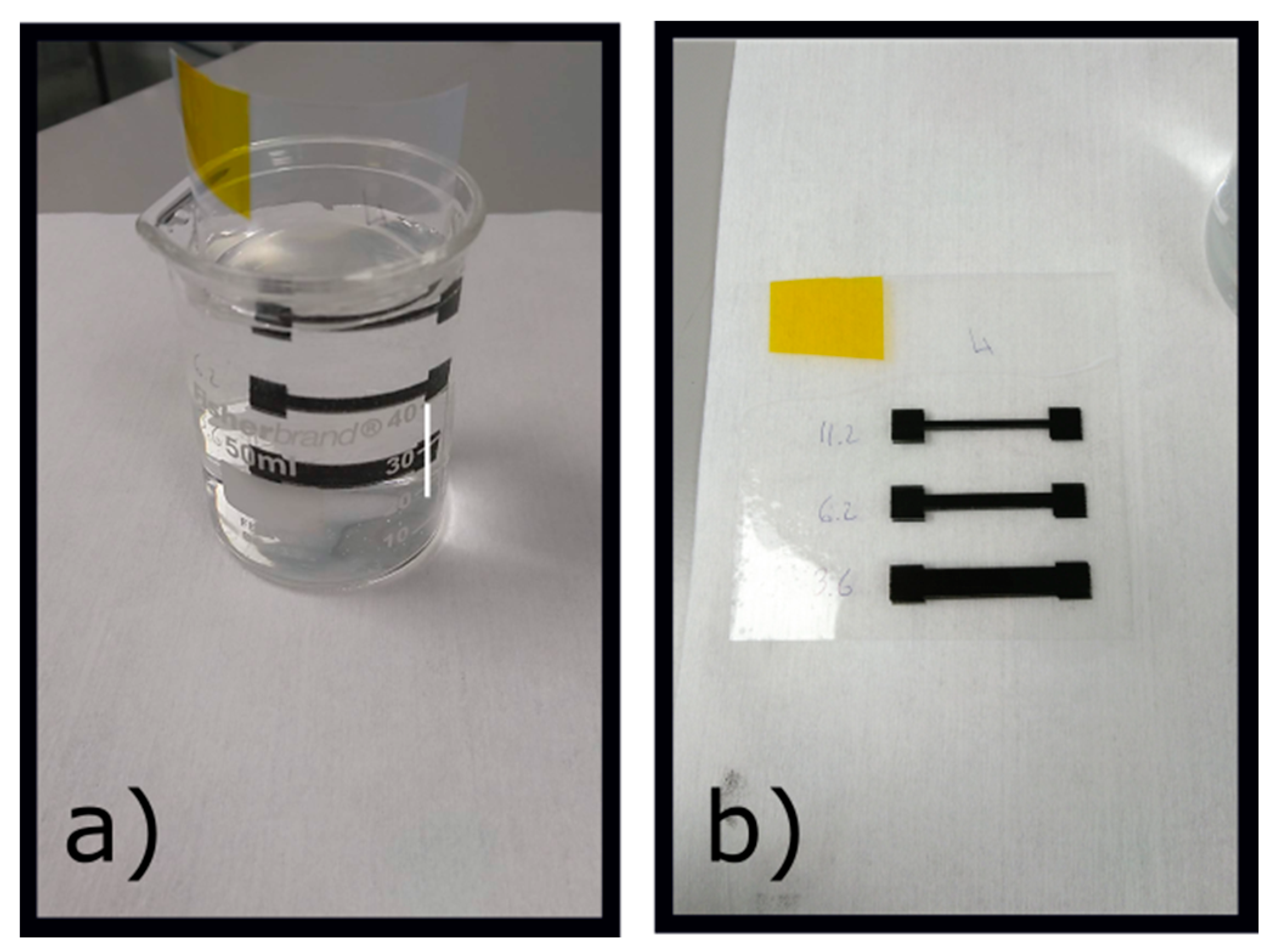

Figure A2.
Spraying phenomenon observed on a pattern printed with a desktop inkjet printer on regular paper using standard coloured pigment ink. (a) The word “United”, printed, (b) zoom on the bottom part of the “i”, and (c) zoom on the bottom left corner of the “i”, showing spraying, comparable to the one observed with the CB ink.


Figure A3.
Droplet mapping profiles of the printed CB-ink on (a) polyethylene terephthalate substrate and (b) paper substrate. (c) Height versus diameter of droplets onto both substrates (PET and paper) revealing the more prominent coffee ring effect found when using paper as a substrate.
Figure A3.
Droplet mapping profiles of the printed CB-ink on (a) polyethylene terephthalate substrate and (b) paper substrate. (c) Height versus diameter of droplets onto both substrates (PET and paper) revealing the more prominent coffee ring effect found when using paper as a substrate.

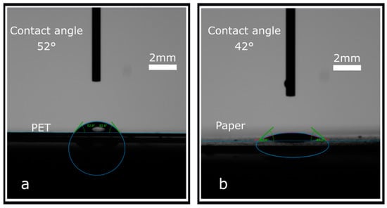
Figure A4.
Water contact angle on (a) polyethylene terephthalate substrate (PET) and (b) paper substrates.
Figure A4.
Water contact angle on (a) polyethylene terephthalate substrate (PET) and (b) paper substrates.
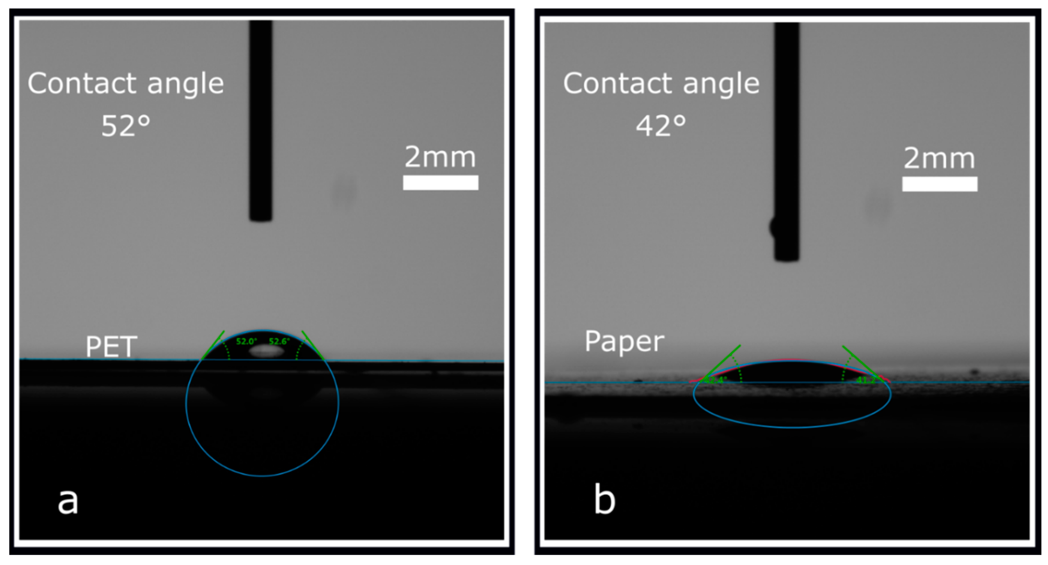
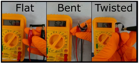
Figure A5.
Conductive ribbons flat, bent, or even twisted.
Figure A5.
Conductive ribbons flat, bent, or even twisted.
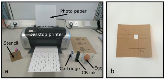
Figure A6.
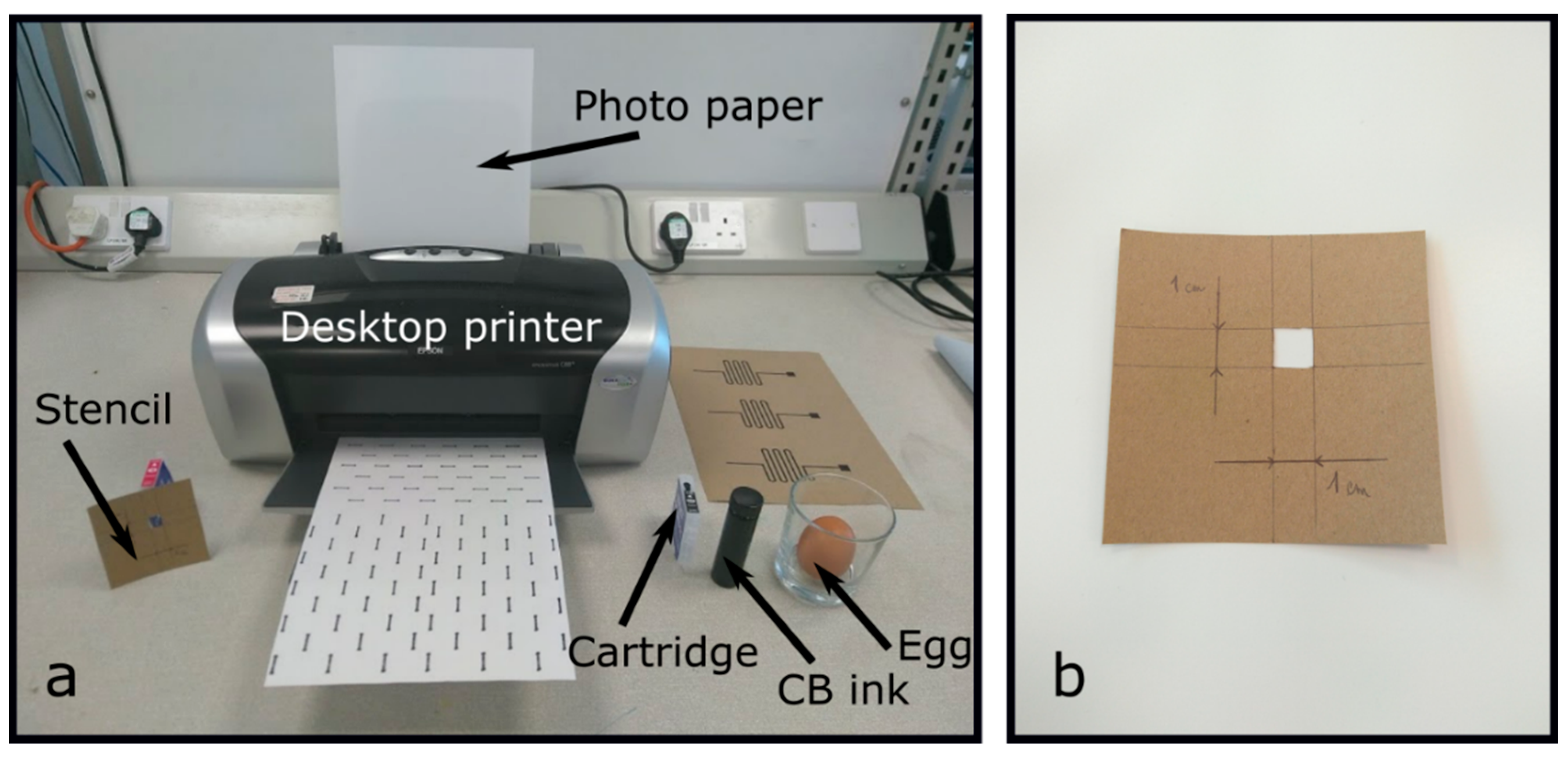
The equipment used for Do-It-Yourself printing of the RC filter. (a) General view of the required apparatus and (b) detail of the stencil used for the screen printing of the egg white. Example line prints and resistors on the white and brown paper observed in the image.
Figure A6.
The equipment used for Do-It-Yourself printing of the RC filter. (a) General view of the required apparatus and (b) detail of the stencil used for the screen printing of the egg white. Example line prints and resistors on the white and brown paper observed in the image.
References
- Prince, J.D. 3D printing: An industrial revolution. J. Electron. Resour. Med. Libr. 2014, 11, 39–45. [Google Scholar] [CrossRef]
- Huang, S.H.; Liu, P.; Mokasdar, A.; Hou, L. Additive manufacturing and its societal impact: A literature review. Int. J. Adv. Manuf. Technol. 2013, 67, 1191–1203. [Google Scholar] [CrossRef]
- Huang, Y.; Leu, M.C.; Mazumder, J.; Donmez, A. Additive manufacturing: Current state, future potential, gaps and needs, and recommendations. J. Manuf. Sci. Eng. 2015, 137, 014001. [Google Scholar] [CrossRef]
- Richardson, M.; Haylock, B. Designer/maker: The rise of additive manufacturing, domestic-scale production and the possible implications for the automotive industry. Comput.-Aided Des. Appl. PACE 2012, 2, 33–48. [Google Scholar] [CrossRef]
- Wilczynski, V. Academic Maker Spaces and Engineering Design; American Society for Engineering Education: Washington, DC, USA, 2015; Volume 26, p. 1. [Google Scholar]
- Browder, R.E.; Aldrich, H.E.; Bradley, S.W. The emergence of the maker movement: Implications for entrepreneurship research. J. Bus. Ventur. 2019. [Google Scholar] [CrossRef]
- Troxler, P. Fabrication laboratories (fab labs). In The Decentralized and Networked Future of Value Creation; Springer: Berlin/Heidelberg, Germany, 2016; pp. 109–127. [Google Scholar]
- Cressey, D. The DIY electronics transforming research. Nat. News 2017, 544, 125. [Google Scholar] [CrossRef] [PubMed]
- Le Borgne, B.; Jacques, E.; Harnois, M. The Use of a Water Soluble Flexible Substrate to Embed Electronics in Additively Manufactured Objects: From Tattoo to Water Transfer Printed Electronics. Micromachines 2018, 9, 474. [Google Scholar] [CrossRef]
- Street, R.A.; Ng, T.; Schwartz, D.E.; Whiting, G.L.; Lu, J.; Bringans, R.; Veres, J. From printed transistors to printed smart systems. Proc. IEEE 2015, 103, 607–618. [Google Scholar] [CrossRef]
- Fukuda, K.; Takeda, Y.; Yoshimura, Y.; Shiwaku, R.; Tran, L.T.; Sekine, T.; Mizukami, M.; Kumaki, D.; Tokito, S. Fully-printed high-performance organic thin-film transistors and circuitry on one-micron-thick polymer films. Nat. Commun. 2014, 5, 4147. [Google Scholar] [CrossRef]
- Cui, Z. Printed Electronics: Materials, Technologies and Applications; John Wiley & Sons: Hoboken, NJ, USA, 2016. [Google Scholar]
- Robin, M.; Kuai, W.; Amela-Cortes, M.; Cordier, S.; Molard, Y.; Mohammed-Brahim, T.; Jacques, E.; Harnois, M. Epoxy based ink as versatile material for inkjet-printed devices. ACS Appl. Mater. Interfaces 2015, 7, 21975–21984. [Google Scholar] [CrossRef]
- Shen, W.; Zhang, X.; Huang, Q.; Xu, Q.; Song, W. Preparation of solid silver nanoparticles for inkjet printed flexible electronics with high conductivity. Nanoscale 2014, 6, 1622–1628. [Google Scholar] [CrossRef] [PubMed]
- Tao, Z.; Le Borgne, B.; Mohammed-Brahim, T.; Jacques, E.; Harnois, M. Spreading and drying impact on printed pattern accuracy due to phase separation of a colloidal ink. Colloid Polym. Sci. 2018, 296, 1749–1758. [Google Scholar] [CrossRef]
- Soltman, D.; Subramanian, V. Inkjet-printed line morphologies and temperature control of the coffee ring effect. Langmuir 2008, 24, 2224–2231. [Google Scholar] [CrossRef] [PubMed]
- Derby, B. Inkjet printing of functional and structural materials: Fluid property requirements, feature stability, and resolution. Annu. Rev. Mater. Res. 2010, 40, 395–414. [Google Scholar] [CrossRef]
- Ko, S.H.; Pan, H.; Grigoropoulos, C.P.; Luscombe, C.K.; Fréchet, J.M.; Poulikakos, D. All-inkjet-printed flexible electronics fabrication on a polymer substrate by low-temperature high-resolution selective laser sintering of metal nanoparticles. Nanotechnology 2007, 18, 345202. [Google Scholar] [CrossRef]
- Calvert, P. Inkjet printing for materials and devices. Chem. Mater. 2001, 13, 3299–3305. [Google Scholar] [CrossRef]
- De Gans, B.-J.; Kazancioglu, E.; Meyer, W.; Schubert, U.S. Ink-jet printing polymers and polymer libraries using micropipettes. Macromol. Rapid Commun. 2004, 25, 292–296. [Google Scholar] [CrossRef]
- Jang, D.; Kim, D.; Moon, J. Influence of fluid physical properties on ink-jet printability. Langmuir 2009, 25, 2629–2635. [Google Scholar] [CrossRef]
- Deegan, R.D.; Bakajin, O.; Dupont, T.F.; Huber, G.; Nagel, S.R.; Witten, T.A. Capillary flow as the cause of ring stains from dried liquid drops. Nature 1997, 389, 827. [Google Scholar] [CrossRef]
- Peng, X.; Yuan, J.; Shen, S.; Gao, M.; Chesman, A.S.; Yin, H.; Cheng, J.; Zhang, Q.; Angmo, D. Perovskite and organic solar cells fabricated by inkjet printing: Progress and prospects. Adv. Funct. Mater. 2017, 27, 1703704. [Google Scholar] [CrossRef]
- Van der Vaart, N.; Lifka, H.; Budzelaar, F.; Rubingh, J.; Hoppenbrouwers, J.; Dijksman, J.; Verbeek, R.; Van Woudenberg, R.; Vossen, F.; Hiddink, M.; et al. Towards large-area full-color active-matrix printed polymer OLED television. J. Soc. Inf. Disp. 2005, 13, 9–16. [Google Scholar] [CrossRef]
- Moon, S.J.; Robin, M.; Wenlin, K.; Yann, M.; Bae, B.S.; Mohammed-Brahim, T.; Jacques, E.; Harnois, M. Morphological impact of insulator on inkjet-printed transistor. Flex. Print. Electron. 2017, 2, 035008. [Google Scholar] [CrossRef]
- Fukuda, K.; Sekine, T.; Kumaki, D.; Tokito, S. Profile control of inkjet printed silver electrodes and their application to organic transistors. ACS Appl. Mater. Interfaces 2013, 5, 3916–3920. [Google Scholar] [CrossRef] [PubMed]
- Goosey, M. End-of-life electronics legislation—An industry perspective. Circuit World 2004, 30, 41–45. [Google Scholar] [CrossRef]
- Irimia-Vladu, M.; Sariciftci, N.S.; Bauer, S. Exotic materials for bio-organic electronics. J. Mater. Chem. 2011, 21, 1350–1361. [Google Scholar] [CrossRef]
- Stavrinidou, E.; Gabrielsson, R.; Gomez, E.; Crispin, X.; Nilsson, O.; Simon, D.T.; Berggren, M. Electronic plants. Sci. Adv. 2015, 1, e1501136. [Google Scholar] [CrossRef] [PubMed]
- Tao, Z.; Mohammed-Brahim, T.; Lei, W.; Harnois, M.; Jacques, E. Impact of the post-thermal annealing on OFETs using printed contacts, printed organic gate insulator and evaporated C60 active layer. Solid-State Electron. 2018, 150, 51–59. [Google Scholar] [CrossRef]
- Kalb, W.L.; Mathis, T.; Haas, S.; Stassen, A.F.; Batlogg, B. Organic small molecule field-effect transistors with CytopTM gate dielectric: Eliminating gate bias stress effects. Appl. Phys. Lett. 2007, 90, 092104. [Google Scholar] [CrossRef]
- Lu, Y.; Fujii, M. Dielectric analysis of hen egg white with denaturation and in cool storage. Int. J. Food Sci. Technol. 1998, 33, 393–399. [Google Scholar] [CrossRef]
- Irimia-Vladu, M. “Green” electronics: Biodegradable and biocompatible materials and devices for sustainable future. Chem. Soc. Rev. 2014, 43, 588–610. [Google Scholar] [CrossRef] [PubMed]
- Bibi, F.; Villain, M.; Guillaume, C.; Sorli, B.; Gontard, N. A review: Origins of the dielectric properties of proteins and potential development as bio-sensors. Sensors 2016, 16, 1232. [Google Scholar] [CrossRef] [PubMed]
- Wu, G.; Feng, P.; Wan, X.; Zhu, L.; Shi, Y.; Wan, Q. Artificial synaptic devices based on natural chicken albumen coupled electric-double-layer transistors. Sci. Rep. 2016, 6, 23578. [Google Scholar] [CrossRef] [PubMed]
- Zhou, Y.; Fuentes-Hernandez, C.; Khan, T.M.; Liu, J.-C.; Hsu, J.; Shim, J.W.; Dindar, A.; Youngblood, J.P.; Moon, R.J.; Kippelen, B. Recyclable organic solar cells on cellulose nanocrystal substrates. Sci. Rep. 2013, 3, 1536. [Google Scholar] [CrossRef] [PubMed]
- Glowacki, E.D.; Leonat, L.; Voss, G.; Bodea, M.; Bozkurt, Z.; Irimia-Vladu, M.; Bauer, S.; Sariciftci, N.S. Natural and nature-inspired semiconductors for organic electronics. In Organic Semiconductors in Sensors and Bioelectronics IV; International Society for Optics and Photonics, SPIE Digital Library: Sergy-Pontoise, France, 2011; Volume 8118, p. 81180M. [Google Scholar]
- Chiappini, C.; Liu, X.; Fakhoury, J.R.; Ferrari, M. Biodegradable porous silicon barcode nanowires with defined geometry. Adv. Funct. Mater. 2010, 20, 2231–2239. [Google Scholar] [CrossRef] [PubMed]
- Petritz, A.; Wolfberger, A.; Fian, A.; Irimia-Vladu, M.; Haase, A.; Gold, H.; Rothländer, T.; Griesser, T.; Stadlober, B. Cellulose as biodegradable high-k dielectric layer in organic complementary inverters. Appl. Phys. Lett. 2013, 103, 191_1. [Google Scholar] [CrossRef]
- Capelli, R.; Amsden, J.J.; Generali, G.; Toffanin, S.; Benfenati, V.; Muccini, M.; Kaplan, D.L.; Omenetto, F.G.; Zamboni, R. Integration of silk protein in organic and light-emitting transistors. Org. Electron. 2011, 12, 1146–1151. [Google Scholar] [CrossRef] [PubMed]
- Le Borgne, B.; De Sagazan, O.; Crand, S.; Jacques, E.; Harnois, M. Conformal Electronics Wrapped Around Daily Life Objects Using an Original Method: Water Transfer Printing. ACS Appl. Mater. Interfaces 2017, 9, 29424–29429. [Google Scholar] [CrossRef]
- Le Borgne, B.; Liu, S.; Morvan, X.; Crand, S.; Sporea, R.A.; Lu, N.; Harnois, M. Water Transfer Printing Enhanced by Water-Induced Pattern Expansion: Toward Large-Area 3D Electronics. Adv. Mater. Technol. 2019. [Google Scholar] [CrossRef]
- Fukuhira, Y.; Kitazono, E.; Hayashi, T.; Kaneko, H.; Tanaka, M.; Shimomura, M.; Sumi, Y. Biodegradable honeycomb-patterned film composed of poly (lactic acid) and dioleoylphosphatidylethanolamine. Biomaterials 2006, 27, 1797–1802. [Google Scholar] [CrossRef]
- Martins, R.F.; Ahnood, A.; Correia, N.; Pereira, L.M.; Barros, R.; Barquinha, P.M.; Costa, R.; Ferreira, I.M.; Nathan, A.; Fortunato, E.E. Recyclable, flexible, low-power oxide electronics. Adv. Funct. Mater. 2013, 23, 2153–2161. [Google Scholar] [CrossRef]
- Muskovich, M.; Bettinger, C.J. Biomaterials-based electronics: Polymers and interfaces for biology and medicine. Adv. Healthc. Mater. 2012, 1, 248–266. [Google Scholar] [CrossRef] [PubMed]
- King, S.G.; Castaldelli, E.; McCaffterty, L.; Silva, S.R.P.; Stolojan, V. Micro-Centrifugal Technique for Improved Assessment and Optimization of Nanomaterial Dispersions: The Case for Carbon Nanotubes. ACS Appl. Nano Mater. 2018, 1, 6217–6225. [Google Scholar] [CrossRef]
- Limousy, L.; Jeguirim, M.; Labbe, S.; Balay, F.; Fossard, E. Performance and emissions characteristics of compressed spent coffee ground/wood chip logs in a residential stove. Energy Sustain. Dev. 2015, 28, 52–59. [Google Scholar] [CrossRef]
- Bach, C.; Dauchy, X.; Etienne, S. Characterization of poly (ethylene terephthalate) used in commercial bottled water. In IOP Conference Series: Materials Science and Engineering; IOP Publishing: Bristol, UK, 2009; Volume 5, p. 012005. [Google Scholar]
- Ajji, A.; Chapleau, N. Structure and properties of impact modified polyethylene terephthalate. J. Mater. Sci. 2002, 37, 3893–3901. [Google Scholar] [CrossRef]
- McGuigan, A.; Briggs, G.; Burlakov, V.; Yanaka, M.; Tsukahara, Y. An elastic–plastic shear lag model for fracture of layered coatings. Thin Solid Films 2003, 424, 219–223. [Google Scholar] [CrossRef]
© 2019 by the authors. Licensee MDPI, Basel, Switzerland. This article is an open access article distributed under the terms and conditions of the Creative Commons Attribution (CC BY) license (http://creativecommons.org/licenses/by/4.0/).


