Article

Compact and Low Crosstalk Echelle Grating Demultiplexer on Silicon-On-Insulator Technology

Advanced Electronics and Photonics Research Centre, National Research Council Canada, Ottawa, ON K1A 0R6, Canada
*
Author to whom correspondence should be addressed.
Electronics 2019, 8(6), 687; https://doi.org/10.3390/electronics8060687
Submission received: 7 May 2019 / Revised: 12 June 2019 / Accepted: 13 June 2019 / Published: 18 June 2019
(This article belongs to the Special Issue Optical Communications and Networks)

Abstract

:
We report on the design of an ultra-compact integrated wavelength demultiplexer in echelle configuration for the optical O-band realized on silicon-on-insulator technology. The device has four channels with channel spacing of 800 GHz and a small footprint of 260 × 83 μm2. Channel crosstalk lower than −28 dB across the four channels is experimentally demonstrated along with insertion losses of −1.5 dB.

1. Introduction

Silicon-on-insulator (SOI) photonic devices are becoming a cornerstone of modern optical fiber communication systems. The possibility to integrate on a chip-size circuit many components (e.g., waveguides, chip-fiber couplers, (de)multiplexers, phase shifters, high-speed modulators, and photodetectors) allows a considerable reduction in the size of optical modules, improves their stability and reduces operational power and cost [1,2]. The high index contrast provided by SOI technologies enables high integration density of components and complex circuit architecture. For short and medium reach communication, the use of the optical O-band (1260 nm to 1360 nm) is often preferred. For this wavelength range optical fibers exhibit a lower dispersion, enabling higher data rates and longer transmission distances without the use of dispersion compensation technologies that, albeit available, would significantly increase the cost and complexity of the communication system [3]. Wavelength division multiplexing (WDM) is a key technology for increasing the transmission data rate within an optical fiber by using multiple carrier wavelengths, modulated with different data streams. These wavelengths are multiplexed and demultiplexed by using optical filters that must guarantee low insertion loss and especially high inter-channel isolation to ensure low crosstalk [4].
Several SOI device configurations are reported in the literature for wavelength (de)multiplexing, including arrayed waveguide gratings [5], Mach–Zehnder cascaded filters [6], ring resonators [7] and echelle gratings [8,9,10]. Compared to other devices, in echelle gratings the phase delays are induced in a slab waveguide rather than in laterally-confined waveguides. In fabricated devices feature width control and uniformity hence do not contribute to phase errors, which are as a result mostly determined only by non-uniformities in the thickness of the slab waveguide core layer and fluctuations in the position and definition of the grating facets [11]. This gives echelle gratings an advantage over devices based on laterally-confined waveguides such as arrayed waveguide gratings, especially for moderate to large channel spacing [12]. In this situation echelle grating designs with a compact footprint can be achieved [13], minimizing phase errors due to fabrication variability and improving crosstalk and insertion loss performance [14,15,16,17,18].
In demultiplexers based on echelle gratings, polarization compensators can be included in the slab region of the device to reduce performance dependence on polarization if both polarizations are employed [15,19,20]. Flat-top transmission and reduced channel crosstalk can be achieved for example by using multi-mode input waveguides [4,21] or modified (dithered) gratings producing essentially a double image of the input light on the output waveguides [22]. Temperature dependence of the echelle grating transfer function can be compensated using a temperature-synchronized input [23].
In this paper we report the design and experimental demonstration of an ultra-compact 1 × 4 wavelength demultiplexer for the optical O-band with channel spacing of 800 GHz featuring a channel crosstalk lower than −28 dB. The device is realized on an SOI platform with a thin silicon layer, featuring an overall footprint (including input and output waveguides) of 260 × 83 μm2. This device is among the most compact echelle gratings with similar performance yet reported in the literature.

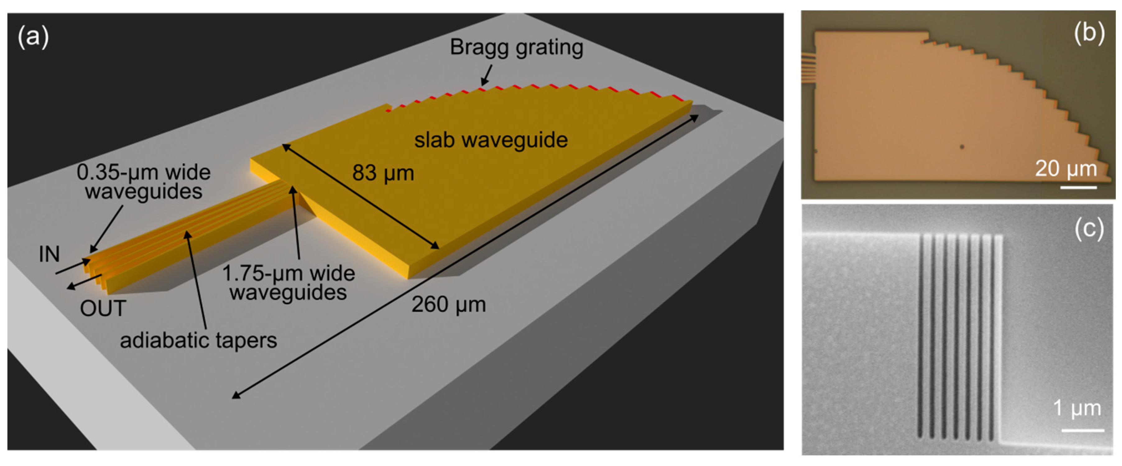
2. Design and Simulation of the Echelle Grating Demultiplexer

We consider here an echelle grating in a classical Rowland mounting (see Figure 1a). Light from a fully-etched input waveguide laterally diverges in a silicon slab waveguide and illuminates a concave grating. The waveguides are adiabatically widened in order to reduce the diffraction angle spread and hence the grating length and optical aberration effects, as discussed below. The grating diffracts the light backward in the slab and produces an image of the input light on a plane where output waveguides are located—here the edge of the slab just below the input waveguide [9,16,22]. Different wavelengths produce images at different positions.
The phase relation required to obtain constructive interference between the light reflected by adjacent grating facets determines the angle of the reflected light beam φ with respect to the grating normal according to the scalar grating equation:
sin ϑ + sin φ = m λ n eff ( λ ) Λ
where ϑ is the angle of the incident beam with respect to the grating normal, m is the diffraction order, λ is the wavelength in vacuum, neff is the (wavelength dependent) effective index of the slab mode, and Λ is the grating period. For a Rowland circle configuration and including the slab effective index dispersion, the following relation for grating linear dispersion D is obtained [9,16]:
D   =   2 R ( sin ϑ + sin φ ) λ ( 1 λ n eff d n eff d λ ) ,
where R is the radius of the Rowland circle. D represents the linear variation of the focal position in the echelle image plane per unit variation of light wavelength. From Equations (1) and (2) it follows that grating dispersion—and hence output waveguide separation—increases with the radius of Rowland circle and grating order.
We designed a 1 × 4 demultiplexer with channel spacing of 800 GHz (about 4.6 nm) aligned with the wavelength grid proposed by the IEEE 802.3 working group for optical datacenter communications based on WDM technology [24]. An SOI platform with a core thickness of 220 nm and only fully etched channel waveguides was chosen to ease fabrication with a single etch step. The design was optimized for TE polarized modes. The design and simulation of the echelle grating were performed with a dedicated 2D semi-vectorial in-house tool based on the Huygens–Kirchhoff diffraction theory and the effective index approximation. We considered an effective refractive index of the fundamental TE-polarized slab mode neff = 2.997 at λ = 1300 nm with a wavelength derivative dneff/ = −0.67 μm−1. The design used two stigmatic points [8] placed at the locations of the second and third output waveguides.
For echelle gratings in the high index contrast SOI platform with a thin core layer, the channel crosstalk mainly originates from slab thickness inhomogeneity [11,25] and errors in the position of grating facets compared to their designed location [16]. This fabrication variability distorts the light phase and amplitude distributions along the image plane of the grating, increasing undesired light coupling in adjacent spectral channels. A small device footprint can be used to reduce the impact of these variabilities and phase errors, improving the crosstalk achieved in practice [11]. On the other hand, reducing the Rowland radius comes with several drawbacks. A small radius reduces the grating linear dispersion, as shown in Equation (2), and imposes small waveguide width and separation. Eventually this degrades the crosstalk through evanescent coupling when the waveguide width and gap become too small. Moreover, a narrow input waveguide increases the beam diffraction angle in the slab, requiring a long grating (hence echelle footprint) in order to capture the input light. A short grating truncates the tails of the diffracted field and introduces deformations in the image plane in the form of side lobes which increase the crosstalk. The field truncation also contributes to stray light and losses. Lastly, a small Rowland radius reduces the size of the grating facets and waveguide gaps, making fabrication more challenging and possibly increasing other undesired effects, e.g., corner diffraction and rounding. Some of these issues can be mitigated by increasing the grating order which in turn increases the size of grating facets (by increasing the grating period, see Equation (1)). Wide grating facets, however, increase the filter roll-off, degrading channel uniformity.
Based on the previous arguments, for the current design we selected a small Rowland radius of R = 129 μm, a grating order m = 35, and a width of 1.75 μm for the input waveguide and the four output waveguides. The center-to-center distance between the waveguides at the edge of the slab varied from 2.2 μm to 2 μm. Crosstalk due to evanescent coupling was estimated to be negligible compared to the crosstalk due to the echelle grating. Adiabatic tapers (75-μm-long) (see Figure 1a) were used to connect input and output waveguides to single-mode access waveguides with a width of 0.35 μm. The input waveguide was at an angle of ϑ = 62 ° while output waveguides were centered around φ = 60°. The grating angular width was set to 14°, requiring 17 facets. The final echelle grating footprint was 188 × 83 μm2 while device footprint including input and output tapers was 260 × 83 μm2.
The simulated transfer functions of the four output channels of the echelle demultiplexer are shown in Figure 2a, assuming that the grating facets have 100% reflectivity. In practice a high reflectivity was achieved with Bragg grating reflectors, as discussed in the next section. The four channels were centered at 1295.6 nm, 1300.0 nm, 1304.6 nm, and 1309.1 nm [24]. Insertion losses had values between −1.2 dB and −0.6 dB, yielding a channel uniformity (roll-off) better than 0.6 dB across the whole spectrum. The 1-dB bandwidth of the channels was between 224 GHz and 236 GHz and the free spectral range was 28.8 nm. A theoretical crosstalk of about −40 dB was predicted. We also investigated the impact of random phase errors on the device crosstalk. We assumed for each facet an independent random phase fluctuation uniformly distributed within a range of ±0.15 rad. The fluctuation was equivalent to an error in the position of the facets of about ±5 nm or to a non-uniformity of the mode effective refractive index across the slab of ±10−4 [16]. This non-uniformity of the effective index corresponded to a sub-nanometer variability of the slab thickness, which was in agreement with common manufacturing variability for the small area of the device [26]. Taking into account these phase errors the maximum channel crosstalk was expected to be about −30 dB.

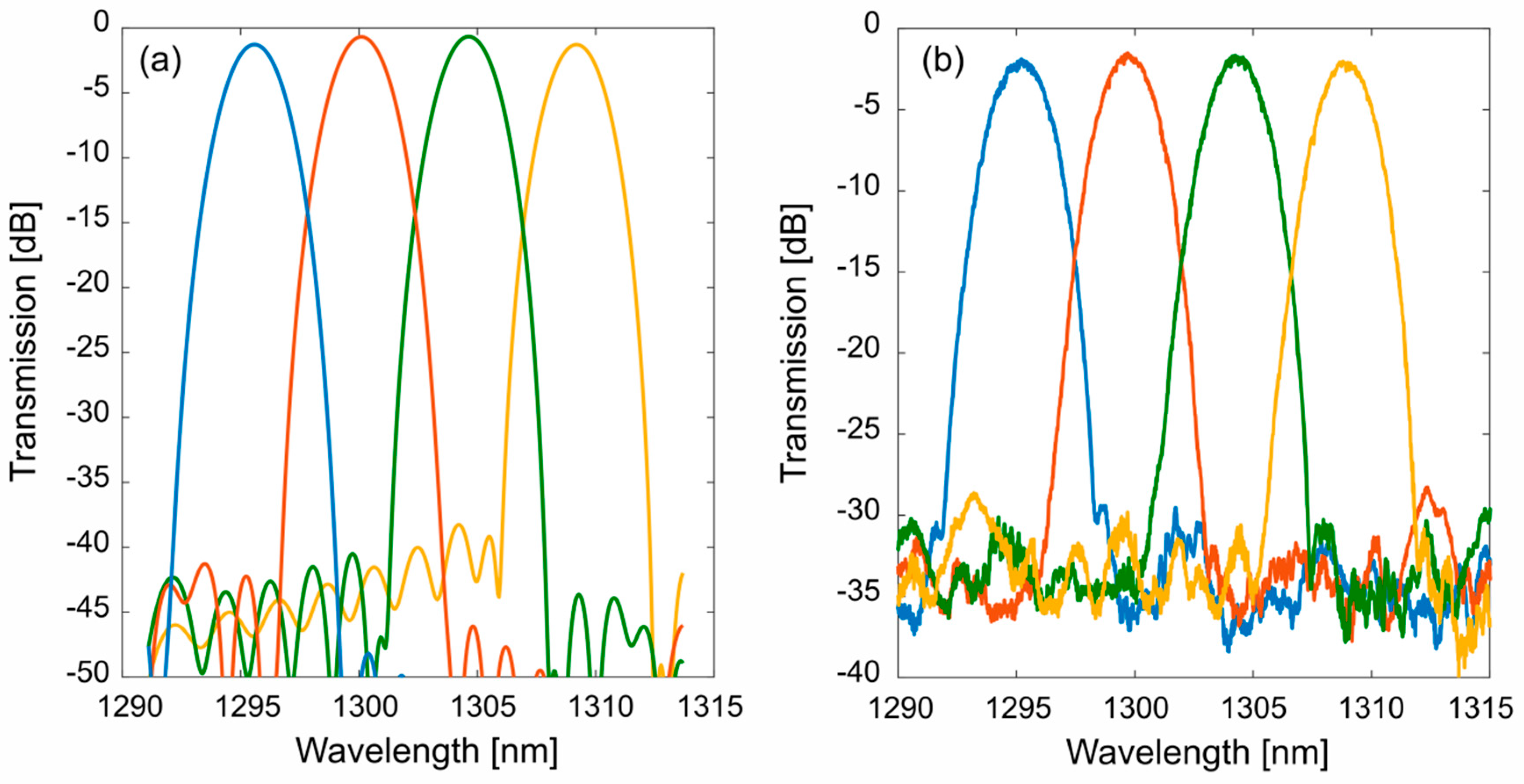
3. Fabrication and Experimental Results

Samples were fabricated with an SOI single-etch technology on a substrate with 220 nm silicon and 3-µm-thick buried oxide (BOX) layer. The waveguide pattern was defined by electron beam lithography using hydrogen silsesquioxane (HSQ) resist and inductively coupled (ICP) high density plasma etching. The waveguides were then coated with a 3-µm-thick SiO2 film by plasma enhanced chemical vapor (PECVD) deposition. Four copies of the same design were fabricated on two different samples during the same fabrication run. Devices 1 and 2 were fabricated side by side on the same sample while devices 3 and 4 were on another sample. A photograph of one of the fabricated devices taken with an optical microscope is shown in Figure 1b. Two additional waveguides were added near the designed input waveguide for reliability and test purposes but were not used during the experiments.
As mentioned in the previous section, Bragg grating reflectors were used at the grating facets. The reflector gratings were fully etched with a period of 285 nm and duty cycle of 0.65. They consisted of seven periods and had a calculated reflectivity of 0.97 at the design wavelength and above 0.9 from λ = 1200 nm to λ = 1600 nm, making them robust to fabrication variations. Reflectivity was experimentally measured on dedicated test structures to be about 0.91 (−0.4 dB) at λ = 1300 nm. A scanning electron microscope picture of the Bragg grating reflector used for each facet is shown in Figure 1c.
The performance of the demultiplexer was measured by coupling light from a tunable semiconductor laser in and out of the chip using high-efficiency subwavelength grating metamaterial edge couplers [27,28]. Input and output lensed polarization-maintaining optical fibers with a Gaussian beam waist of about 3 μm were used. The input polarization was set to TE using a pigtailed half-wave plate polarization rotator. Losses due to the polarization optics system, optical fibers, edge couplers, and on-chip propagation were determined for each fabricated device through a set of reference waveguides running close to the echelle demultiplexer. On average the reference loss was −7 dB, of which −2.5 dB was due to the optical setup and the remaining −5.5 dB represented the insertion loss of the chip (fiber coupling and waveguide propagation losses).
The measured transmittance spectra for the four channels (output waveguides) of one of the fabricated echelle grating demultiplexers (device 2) are shown in Figure 2b. Data have been normalized using the average reference loss. The channels were centered at 1295.2 nm, 1299.7 nm, 1304.2 nm, and 1308.8 nm. The channel spacing was 800 GHz as designed and the 1-dB bandwidth was between 210 GHz and 225 GHz. The excess losses (after reference loss normalization) were −1.9 dB, −1.5 dB, −1.7 dB, and −2.0 dB, respectively, with a roll-off of less than −0.5 dB across the measured spectrum. Channel crosstalk was measured in a 1-nm wavelength range around the channel maximum and was between −28.3 dB and −28.9 dB for all four channels. Table 1 reports the results in terms of echelle insertion loss (after reference loss normalization), roll-off and crosstalk for the four fabricated copies of the device. The performances of the demultiplexer showed a good stability across the different device copies. Insertion losses ranged between −1.4 dB and −1.7 dB; roll-off was about −0.5 dB for three devices and about −1 dB for device 3; channel crosstalk was always below −24 dB.

4. Conclusions

We have presented an ultra-compact echelle grating demultiplexer on silicon-on-insulator technology for the optical O-band. The demultiplexer has four channels with a spacing of 800 GHz in compliance with the wavelength grid proposed for optical datacenter interfaces. The footprint of the device is 260 × 83 μm2 including the access waveguide tapers. Insertion losses lower than −1.5 dB, channel uniformity better than 0.5 dB and crosstalk below −28 dB have been experimentally demonstrated. The compact dimensions allowed reducing the phase errors, improving both channel crosstalk and performance repeatability. We believe that the reported device represents a useful building block for improving the compactness and scalability of components for future short and medium reach optical networks.

Author Contributions

P.G.V., A.D., P.C. and D.-X.X. conceived the device. A.D. and P.G.V. developed the design and simulation software. J.H.S., S.J. and J.L. provided support during the design and fabrication. S.W. performed the experiments. D.M. analyzed the data. All authors contributed to the discussion and manuscript preparation.

Funding

This research received no external funding.

Conflicts of Interest

The authors declare no conflict of interest.

References

  1. Thomson, D.; Zilkie, A.; Bowers, J.E.; Komljenovic, T.; Reed, G.T.; Vivien, L.; Marris-Morini, D.; Cassan, E.; Virot, L.; Fédéli, J.M.; et al. Roadmap on silicon photonics. J. Opt. 2016, 18, 073003. [Google Scholar] [CrossRef]
  2. Vivien, L. (Ed.) Handbook of Silicon Photonics; CRC Press: Boca Raton, FL, USA, 2013. [Google Scholar]
  3. Effenberger, F.J. Industrial Trends and Roadmap of Access. J. Light. Technol. 2017, 35, 1142–1146. [Google Scholar] [CrossRef]
  4. Sciancalepore, C.; Lycett, R.J.; Dallery, J.A.; Pauliac, S.; Hassan, K.; Harduin, J.; Duprez, H.; Weidenmueller, U.; Gallagher, D.F.; Menezo, S.; et al. Low-Crosstalk Fabrication-Insensitive Echelle Grating Demultiplexers on Silicon-on-Insulator. IEEE Photonics Technol. Lett. 2015, 27, 494–497. [Google Scholar] [CrossRef]
  5. Cheung, S.; Su, T.; Okamoto, K.; Yoo, S.J.B. Ultra-Compact Silicon Photonic 512 × 512 25 GHz Arrayed Waveguide Grating Router. IEEE J. Sel. Top. Quantum Electron. 2014, 20, 310–316. [Google Scholar] [CrossRef]
  6. Horst, F.; Green, W.M.J.; Assefa, S.; Shank, S.M.; Vlasov, Y.A.; Offrein, B.J. Cascaded Mach-Zehnder wavelength filters in silicon photonics for low loss and flat pass-band WDM (de-)multiplexing. Opt. Express 2013, 21, 11652. [Google Scholar] [CrossRef] [PubMed]
  7. Morichetti, F.; Ferrari, C.; Canciamilla, A.; Melloni, A. The first decade of coupled resonator optical waveguides: Bringing slow light to applications. Laser Photonics Rev. 2012, 6, 74–96. [Google Scholar] [CrossRef]
  8. Horst, F.; Green, W.M.J.; Offrein, B.J.; Vlasov, Y.A. Silicon-on-Insulator Echelle Grating WDM Demultiplexers with Two Stigmatic Points. IEEE Photonics Technol. Lett. 2009, 21, 1743–1745. [Google Scholar] [CrossRef]
  9. Brouckaert, J.; Bogaerts, W.; Dumon, P.; Thourhout, D.V.; Baets, R. Planar Concave Grating Demultiplexer Fabricated on a Nanophotonic Silicon-on-Insulator Platform. J. Light. Technol. 2007, 25, 1269–1275. [Google Scholar] [CrossRef] [Green Version]
  10. Brouckaert, J.; Bogaerts, W.; Selvaraja, S.; Dumon, P.; Baets, R.; Thourhout, D.V. Planar Concave Grating Demultiplexer with High Reflective Bragg Reflector Facets. IEEE Photonics Technol. Lett. 2008, 20, 309–311. [Google Scholar] [CrossRef]
  11. Okamoto, K. Progress and technical challenge for planar waveguide devices: Silica and silicon waveguides. Laser Photonics Rev. 2012, 6, 14–23. [Google Scholar] [CrossRef]
  12. Pathak, S.; Dumon, P.; Thourhout, D.V.; Bogaerts, W. Comparison of AWGs and Echelle Gratings for Wavelength Division Multiplexing on Silicon-on-Insulator. IEEE Photonics J. 2014, 6, 1–9. [Google Scholar] [CrossRef]
  13. Dabos, G.; Pitris, S.; Mitsolidou, C.; Alexoudi, T.; Fitsios, D.; Cherchi, M.; Harjanne, M.; Aalto, T.; Kanellos, G.T.; Pleros, N. Thick-SOI Echelle grating for any-to-any wavelength routing interconnection in multi-socket computing environments. In Proceedings of the Optical Interconnects XVII, San Francisco, CA, USA, 28 January–2 February 2017; p. 1010914. [Google Scholar]
  14. Bock, P.J.; Cheben, P.; Delâge, A.; Schmid, J.H.; Xu, D.X.; Janz, S.; Hall, T.J. Demultiplexer with blazed waveguide sidewall grating and sub-wavelength grating structure. Opt. Express 2008, 16, 17616–17625. [Google Scholar] [CrossRef] [PubMed]
  15. Janz, S.; Balakrishnan, A.; Charbonneau, S.; Cheben, P.; Cloutier, M.; Delâge, A.; Dossou, K.; Erickson, L.; Gao, M.; Krug, P.A.; et al. Planar Waveguide Echelle Gratings in Silica-On-Silicon. IEEE Photonics Technol. Lett. 2004, 16, 503–505. [Google Scholar] [CrossRef]
  16. Cheben, P.; Delâge, A.; Janz, S.; Xu, D.-X. Echelle and Arrayed Waveguide Gratings for WDM and Spectral Analysis. In Advances in Information Optics and Photonics; SPIE Press: Washington, WA, USA, 2008; pp. 599–632. [Google Scholar]
  17. Zhang, Y.; Schneider, M.; Karnick, D.; Eisenblätter, L.; Kühner, T.; Weber, M. Low-loss and robust DWDM Echelle grating (de-)multiplexers in SOI technology. In Proceedings of the Optical Components and Materials XVI, San Francisco, CA, USA, 2–7 February 2019; p. 109140J. [Google Scholar]
  18. Pommarede, X.; Hassan, K.; Billondeau, P.; Hugues, V.; Grosse, P.; Charbonnier, B.; Duan, G.-H. 16 × 100 GHz Echelle Grating-Based Wavelength Multiplexer on Silicon-on-Insulator Platform. IEEE Photonics Technol. Lett. 2017, 29, 493–495. [Google Scholar] [CrossRef]
  19. Zhu, N.; Song, J.; Wosinski, L.; He, S. Design of a Polarization-Insensitive Echelle Grating Demultiplexer Based on Silicon Nanophotonic Wires. IEEE Photonics Technol. Lett. 2008, 20, 860–862. [Google Scholar] [CrossRef]
  20. Zhu, N.; Song, J.; Wosinski, L.; He, S.; Thylen, L. Experimental demonstration of a cross-order echelle grating triplexer based on an amorphous silicon nanowire platform. Opt. Lett. 2009, 34, 383. [Google Scholar] [CrossRef]
  21. Feng, D.; Qian, W.; Liang, H.; Kung, C.C.; Fong, J.; Luff, B.J.; Asghari, M. Fabrication Insensitive Echelle Grating in Silicon-on-Insulator Platform. IEEE Photonics Technol. Lett. 2011, 23, 284–286. [Google Scholar] [CrossRef]
  22. Cheben, P. Wavelength dispersive planar waveguide devices: Echelle gratings and arrayed waveguide gratings. In Optical Waveguides: From Theory to Applied Technologies, 1st ed.; Calvo, M.L., Lakshminarayanan, V., Eds.; CRC Press, Taylor & Francis Group: London, UK, 2007. [Google Scholar]
  23. Melati, D.; Verly, P.G.; Delâge, A.; Cheben, P.; Schmid, J.H.; Janz, S.; Xu, D.X. Athermal echelle grating filter in silicon-on-insulator using a temperature-synchronized input. Opt. Express 2018, 26, 28651–28660. [Google Scholar] [CrossRef]
  24. Cole, C. 100-Gb/s and beyond Ethernet optical interfaces. In Proceedings of the OECC 2010 Technical Digest, Sapporo, Japan, 5–9 July 2010; pp. 108–109. [Google Scholar]
  25. Bogaerts, W.; Selvaraja, S.K.; Dumon, P.; Brouckaert, J.; De Vos, K.; Van Thourhout, D.; Baets, R. Silicon-on-Insulator Spectral Filters Fabricated with CMOS Technology. IEEE J. Sel. Top. Quantum Electron. 2010, 16, 33–44. [Google Scholar] [CrossRef]
  26. Xing, Y.; Dong, J.; Dwivedi, S.; Khan, U.; Bogaerts, W. Accurate extraction of fabricated geometry using optical measurement. Photonics Res. 2018, 6, 1008. [Google Scholar] [CrossRef]
  27. Cheben, P.; Schmid, J.H.; Wang, S.; Xu, D.X.; Vachon, M.; Janz, S.; Lapointe, J.; Painchaud, Y.; Picard, M.J. Broadband polarization independent nanophotonic coupler for silicon waveguides with ultra-high efficiency. Opt. Express 2015, 23, 22553. [Google Scholar] [CrossRef]
  28. Cheben, P.; Halir, R.; Schmid, J.H.; Atwater, H.A.; Smith, D.R. Subwavelength integrated photonics. Nature 2018, 560, 565–572. [Google Scholar] [CrossRef]
Figure 1. (a) Schematic of the 1 × 4 silicon-on-insulator (SOI) echelle grating demultiplexer, including the input and output waveguide tapers—from 0.35 μm width (single mode waveguide) to 1.75 μm at the edge of the slab. (b) Optical microscope photograph of one of the fabricated devices and (c) scanning electron microscope picture of the Bragg grating reflector used at the grating facets.
Electronics 08 00687 g001
Figure 2. (a) Simulated and (b) experimental transmission spectra for the four channels of the echelle demultiplexer. Measured insertion losses are −1.5 dB with channel uniformity (roll-off) less than 0.5 dB. Crosstalk is below −28.3 dB for all channels.
Electronics 08 00687 g002
Table 1. Performance of the echelle demultiplexer measured on four different device copies fabricated in the same run.
DeviceInsertion LossRoll-OffCrosstalk
1−1.6 dB−0.5 dB−24.7 dB
2−1.5 dB−0.5 dB−28.3 dB
3−1.4 dB−1.0 dB−24.0 dB
4−1.7 dB−0.5 dB−24.6 dB

