Review

Recent Developments of Dual-Band Doherty Power Amplifiers for Upcoming Mobile Communications Systems

1
SARAS Technology Limited, Leeds LS12 4NQ, UK
2
School of Electrical Engineering and Computer Science, Faculty of Engineering and Informatics, University of Bradford, Bradford BD7 1DP, UK
3
Computer Systems Department, Ninevah Technical Institute, Northern Technical University, 41001 Mosul, Iraq
*
Authors to whom correspondence should be addressed.
Electronics 2019, 8(6), 638; https://doi.org/10.3390/electronics8060638
Submission received: 15 April 2019 / Revised: 31 May 2019 / Accepted: 2 June 2019 / Published: 6 June 2019
(This article belongs to the Special Issue Recent Technical Developments in Energy-Efficient 5G Mobile Cells)

Abstract

:
Power amplifiers in modern and future communications should be able to handle different modulation standards at different frequency bands, and in addition, to be compatible with the previous generations. This paper reviews the recent design techniques that have been used to operate dual-band amplifiers and in particular the Doherty amplifiers. Special attention is focused on the design methodologies used for power splitters, phase compensation networks, impedance inverter networks and impedance transformer networks of such power amplifier. The most important materials of the dual-band Doherty amplifier are highlighted and surveyed. The main problems and challenges covering dual-band design concepts are presented and discussed. In addition, improvement techniques to enhance such operations are also exploited. The study shows that the transistor parasitic has a great impact in the design of a dual-band amplifier, and reduction of the transforming ratio of the inverter simplifies the dual-band design. The offset line can be functionally replaced by a Π-network in dual-band design rather than T-network.

1. Introduction

The demands for increasing the amount of data that can be transmitted within a limited bandwidth is continuing to grow rapidly, especially with developments, where users are now being attracted by multimedia data and video streaming, as well as the Internet of Things technology revolution. Hence, the 5G mobile generation will include several technologies that can help to achieve its promised goals. Some of these technologies are: beamforming, carrier aggregation, massive multiple input multiple output (MIMO), and more complex modulation schemes, which produce a high peak to average power ratio (PAPR). The high PAPR requires the power amplifier to be backed off from the most efficient point into a region where the efficiency drops sharply to keep the linearity requirements of any communications standard [1,2,3]. Working in the back-off region of the power amplifier means that less efficiency will be obtained, where a large amount of supplied power will be converted into heat [1]. With the simple amplifier, there is inevitably a trade-off between high efficiency and linearity. Modern power amplifiers should be designed to produce high efficiency at a large output power back-off (OBO); known efficiency enhancements techniques include: Doherty power amplifier (DPA), envelope elimination and restoration (EER), envelope tracking (ET), and linear amplification using nonlinear components (LINC), and Chireix out-phasing. However, the simplest technique is the Doherty amplifier, where neither signal processing blocks nor additional controlling circuits are required [4,5,6,7]. Also, new terms have entered the communications systems which are multi-band and multi-mode, where the term “multi-band” refers to a transmitter which works on two different frequency bands simultaneously; in this case, the number of devices, size, and cost will be reduced. On the other hand, the term “multi-mode” refers to a transmitter who can support and combine different access technologies such as 2G, 3G, 4G and 5G on a single platform [8,9,10,11,12,13]. To design a dual-band power amplifier, a hybrid configuration can be used but occupies a large area. Ideally, the power amplifier should be designed to handle multi-band and multi-mode systems concurrently.
This paper, following a brief introduction to the Doherty power amplifier mechanism, reviews the techniques that have been used in designing dual-band Doherty power amplifiers, and finally draws conclusions from this.

2. Classical Doherty Power Amplifier Operation

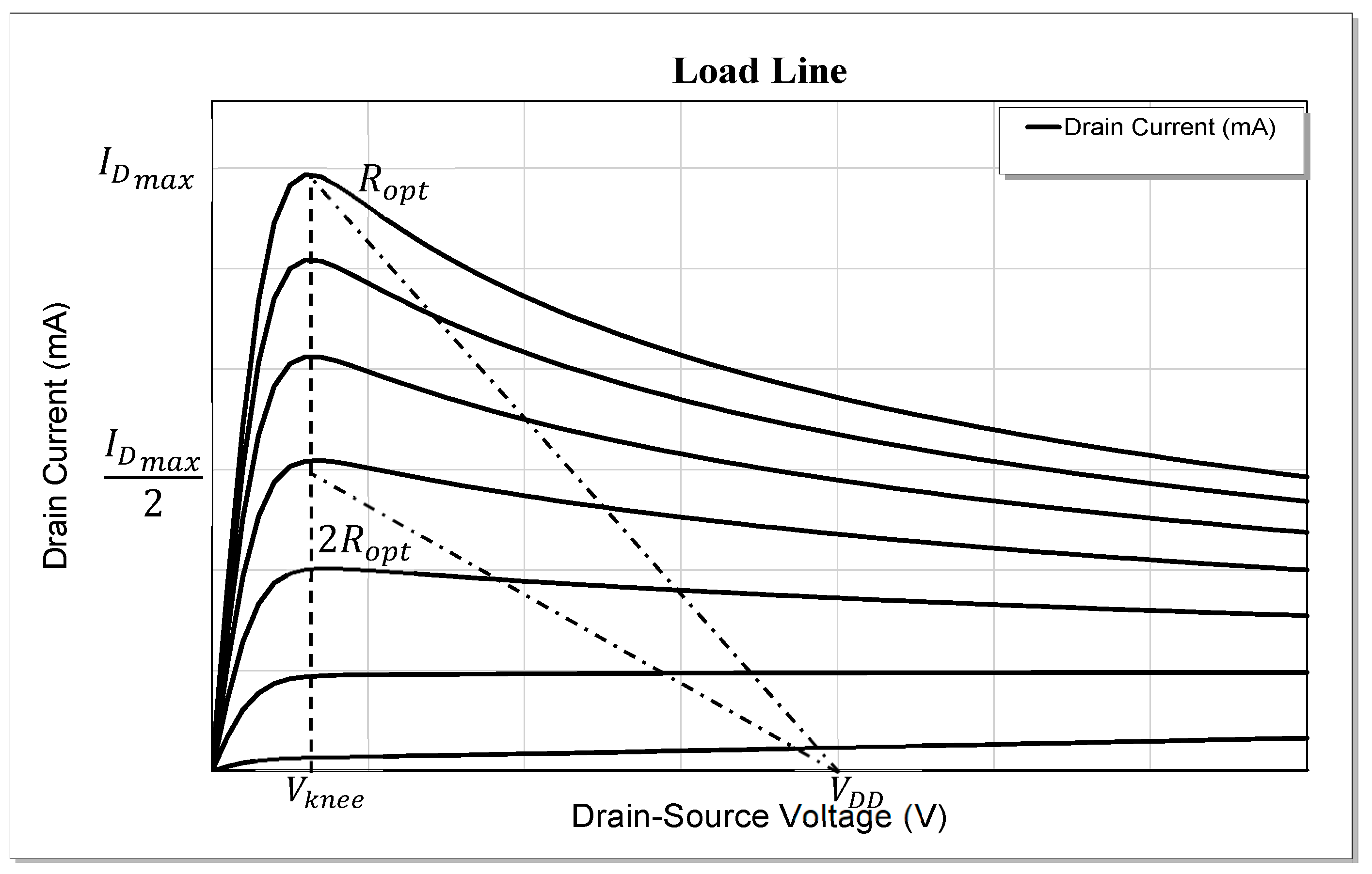
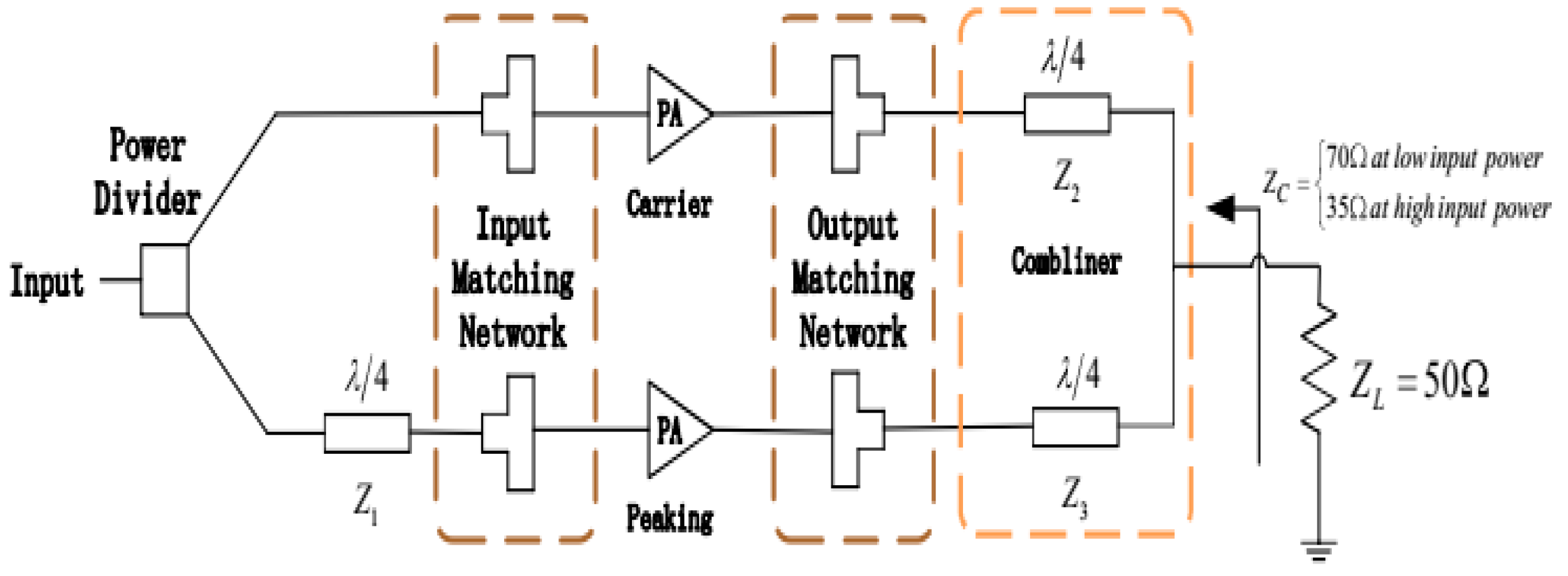
In 1936, W.H. Doherty invented a new combiner designed for broadcasting stations using high power tube amplifiers [5]. A λ/4 transmission lines can be used as a combiner at the output of power amplifiers to achieve a linear output power. The classic DPA consists of two amplifiers known as the carrier (main) amplifier and the auxiliary (peaking) amplifier (Figure 1). A class AB amplifier used for the carrier amplifier whereas a class C amplifier is used for the peaking amplifier. The RF input signal is split between the two amplifiers, where the carrier amplifier is working all the time and should almost reach saturation at the back-off input power due to seeing a high impedance which causes a change in the load-line as shown in Figure 2. At the same power level, the auxiliary amplifier works only in the Doherty region and starts feeding current to the output till it becomes saturated at the peak region, where the two power amplifiers give their maximum designed output power.
The idea of the Doherty amplifier depends on the so-called active load-pull technique [1]. Where the DPA operation can be divided into three regions:
The low RF input power region, where the signal level is not sufficient to turn the auxiliary amplifier on, in this case, the auxiliary amplifier can (theoretically) be represented as an open circuit as shown in Figure 3a. At the same time, the main amplifier is amplifying the input signal as an ordinary power amplifier, however, the load is seen by the main amplifier through the impedance inverter (λ/4 transmission line) and is increased because the characteristic impedance of the λ/4 transmission line is higher than the load impedance. In this case, the main amplifier will be almost saturated because its load line has changed, as illustrated in Figure 2. The impedance seen by the main amplifier depends on the following equation:
Z 1 = Z T 2 R L
where:
  • Z1: the impedance seen by the main amplifier
  • ZT: transmission line characteristic impedance
  • RL: the load
The second region (medium RF input power), where the auxiliary amplifier starts feeding current to the load and acts as an additional current source as illustrated in Figure 3b. As auxiliary amplifier current increases, the apparent load impedance seen by the impedance inverter at the summing node will increase, and hence, the impedance seen by the main amplifier will decrease, and the load line will move as shown in Figure 2. As a result, the output voltage of the main amplifier remains roughly constant, and the total current is increasing which increases the total output power. The following equations show the relationship between the impedance of each amplifier and the amplifiers’ currents:
Z 2 = R L ( 1 + I 1 T I A u x )
Z 1 = Z T 2 R L ( 1 + I A u x I 1 T )
where:
  • Z 2 : the impedance seen by the auxiliary amplifier
  • I 1 T : the current after the λ/4 transmission line
  • I A u x : current of the auxiliary amplifier
Finally, the high-power region, where both amplifiers work at their maximum output current and the impedance seen by each amplifier is controlled also by Equations (2) and (3). The load modulation occurs in the last two regions, where the benefit of Doherty structure is clear.
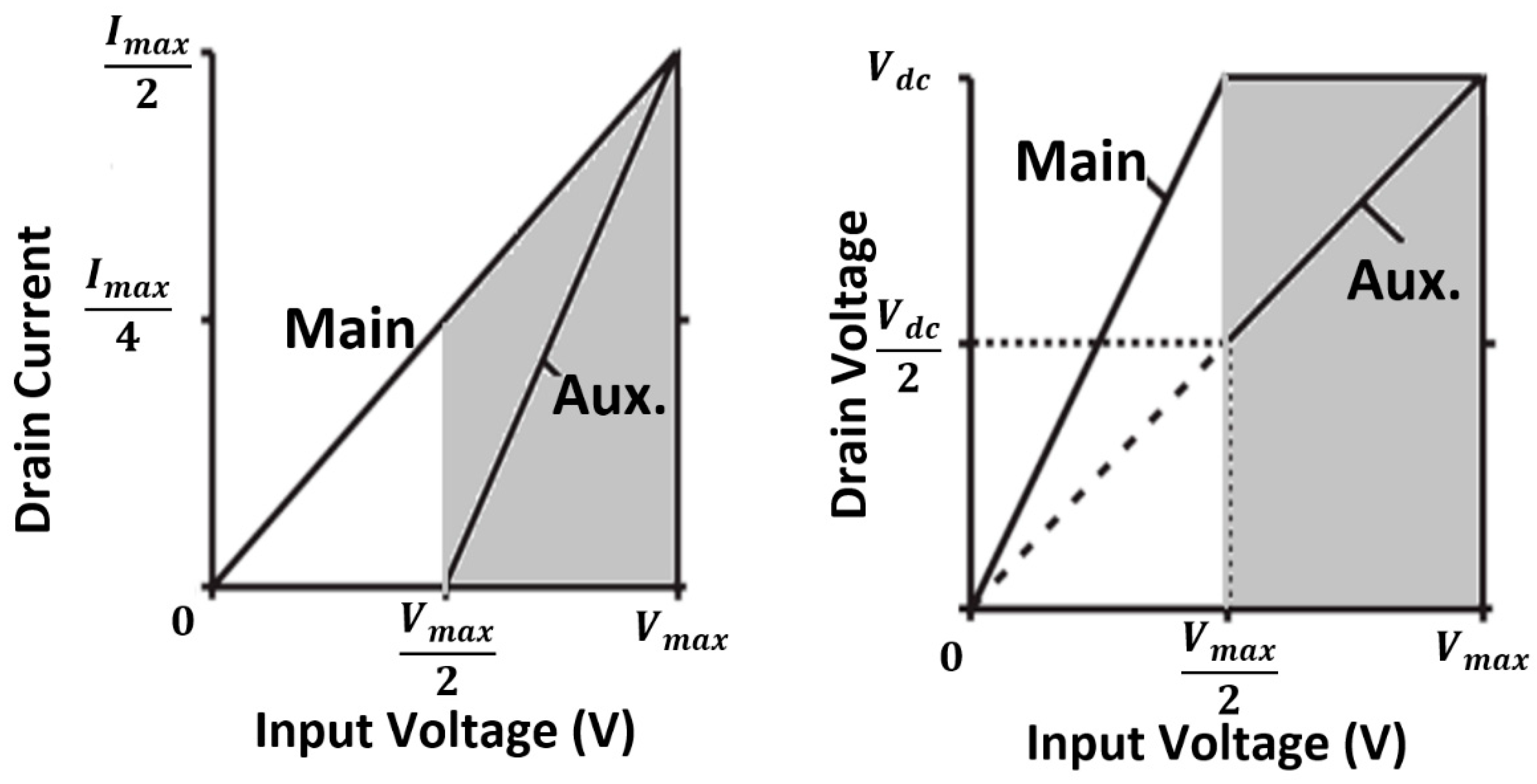
The main and the auxiliary current and voltage behavior is shown in Figure 4. The auxiliary amplifier starts contributing its current near the OBO point, whereas the main amplifier voltage remains roughly constant after the OBO point but its current increases.

3. Dual-Band Doherty Power Amplifier

Wireless communications systems have different standards and requirements where each standard can use a certain frequency band. At the same time, mobile communication systems are being developed where the data rate is one of the main targets for each generation; the growth of data rate requires a complex modulation and more bandwidth [11,12,13,14,15]. However, due to the crowded spectrum, the upcoming generation may use more frequency bands in order to fulfil the targeted requirements (e.g., 5G spectrum consists of three bands are 700 MHz, 3.6 GHz and 26 GHz) [16], in this case, the devices of the new generation should be designed to deal with these frequency bands in addition to the compatibility with the previous mobile generations.
Moreover, a new 3GPP protocol which is narrowband Internet-of-Things (NB-IoT) specifies the maximum output power to be at least 23 dBm for long-range communications [17]. This protocol supports the two frequency bands 699–915 MHz and 1710–1980 MHz; the demand for integrating power amplifiers that can support high power and high efficiency on a chip is increasing since it can increase the battery life and reduce the running cost [17].
In order to increase modulation bandwidth efficiency, carrier aggregation technology was introduced, where new wireless communications systems technologies are expected to use multi-band multi-standard applications [18]. To support dual-band simultaneously, two power amplifiers can be used for each band, but this increases the die area and requires more circuitry to combine their outputs. Therefore, dual-band design can provide a reduction in the size and cost of the system, and Doherty can provide good efficiency [19]. The use of dual-band also requires the PA to work in conjunction with software-defined radio (SDR) [20], which can use the same hardware at two different frequencies to perform a similar function.
The term dual-band can be implemented in two ways; the first is called reconfigurable dual-band amplifier, in this case, the power amplifier is designed to work in two frequency bands, one at a time, where the circuit properties and configuration is changed depending on the target band. On the other hand, the concurrent dual-band implies that the amplifier can work on both frequency bands without any modification or changing of the design; intermodulation distortion should be considered especially if the two bands are close to each other because the effect of device nonlinearity will be significant, in this case, some interference will be introduced to the neighboring channels. The next subsections will deal with dual-band limitations, challenges, and the techniques that were used to make the Doherty power amplifier works in two bands.

3.1. Dual-Band DPA Problems and Challenges

The main problem for multi-band/multi-standard features is the RF-front end-stage [21,22], where RF front-end components such as power amplifiers, filters, antennas, and switches should be designed to work properly on the specified frequency bands to fulfil each standard specification.
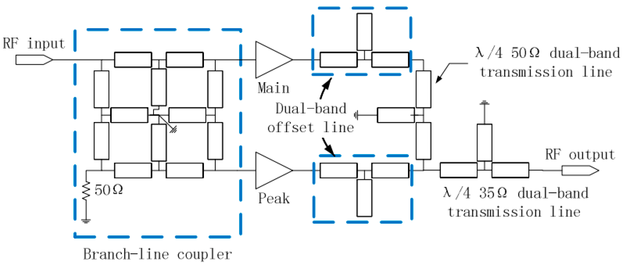
According to [23], as long as there are dual-band components, it is possible to design a multiband DPA. Hence, theoretically, the DPA can be divided into sub-circuits to be analyzed and designed separately. These sub-circuits are the input power splitter, power amplifier design, output power combiner, and the offset lines.
The input power splitter sub-circuit should be designed to achieve the same performance in both bands; a good solution is to use either a branch line coupler (BLC) or a Wilkinson divider, where both types can divide the input power equally or unequally. The main difference between the two types of splitters is the phase difference at the output; where the phase of the two output at Wilkinson will be same, for the branch line the phase difference between the outputs will be 90° [24]. Unfortunately, both types are narrow band solutions because they are frequency-dependent. To provide a dual-band power divider, a broadband power divider can be used to cover the dual-band and ensure that the matching condition is satisfied.
Power amplifier design sub-circuit includes the device cell, input, and output matching networks; the device cell should be capable of working properly at each designed frequency band, which depends on the device characteristics as well as its designed input and output matching networks. In general, the input matching network is responsible for controlling the gain over the required band, whereas the output matching network is responsible for choosing the output power and efficiency. The simulation in [25] showed that the effect of the second harmonic at the input of the PA is negligible so that the input matching network can be designed only for the fundamental frequency at each band. At the same time, the third harmonic also has little effect on the output matching network; hence, the output matching design can consider only the fundamental frequency and the second harmonic at each band [25]. Nevertheless, modern design for matching networks does not depend on the fundamental frequency matching only; further harmonic effects can be included to achieve a certain performance. Moreover, by taking the source-pull and load-pull data with the harmonic effects of a transistor, the required impedance for the transistor can be matched so that good performance can be achieved.
The main limitations of the DPA is the λ/4 quarter wavelength (impedance inverter) and the offset lines which limit the bandwidth due to their natural characteristics [25,26,27,28,29,30], so that to design a DPA that can work in dual-band, the quarter-wave impedance inverter and the offset line should be replaced with more complex networks which give equivalent functions in split bands.

3.2. Π-And T-Networks for Dual-Band DPA

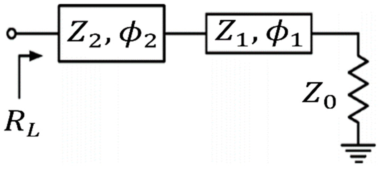
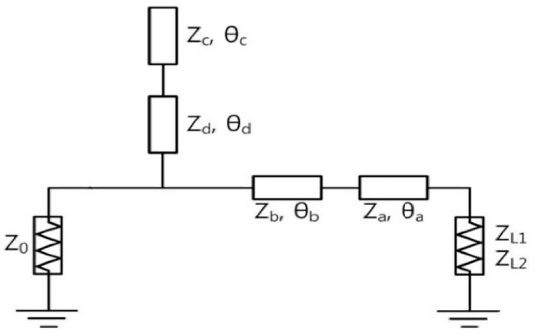
The classic DPA has two simple λ/4 transformers: the impedance inverter and global matching, as shown in Figure 1. These two transmission lines are different in their purpose of work. A simple λ/4 transformer (global matching) can be replaced with a two-section transmission line form which is easily adjusted to give the exact impedance transformation at two frequencies, as shown in Figure 5 (more details of dual-band transformer can be found in [28]). The inherently larger bandwidth of the two sections can be maximized when no matched operation is required between the two operating bands. However, the two-section form cannot be assumed as an impedance inverter, due to the different of work purpose; instead, the impedance inverting section is realized for split band operation as a Π-network by adding two stub sections to a single near-λ/4 section [25].
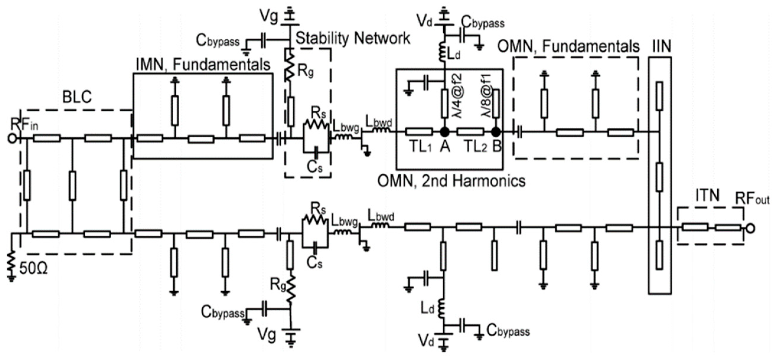
In a comprehensive passive design of a dual-band DPA (1.8 GHz and 2.4 GHz) presented by [25], the design of each amplifier depended on the load-pull/source-pull simulation to find optimum load and source impedances. For dual-band harmonic control, two shunt stub lines in addition to (TL1 and TL2) are used as shown in Figure 6. The first is a short circuit terminated with a length of λ/4 at f2, where it used to cancel the effect of the second harmonic at the upper band at point A, whereas the second with a length of λ/8 at f1 is open to suppress the second harmonic of the lower band at point B. The designed amplifier of [25] was showing good performance.
Additionally, a T-network was used in a dual-band DPA working at 900 MHz and 2000 MHz in [7] as an alternative component for the λ/4 inverter, as shown in Figure 7. In the output matching network, a T-network with a shorted shunt line in addition to an open stub were used [7]; the open stub was used to adjust the phase of output, whereas the T-network with a shorted shunt was used as a dual-band impedance transformer and as a dc feeder at the same time.
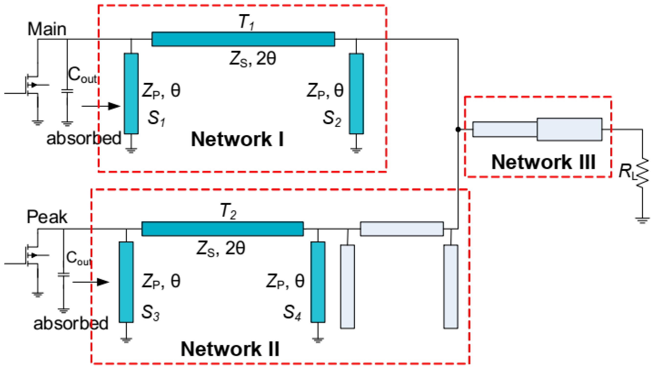
The suggested solutions of using Π- or T-topology in [7,25] were only used for impedance inverters, nevertheless, a modified Π-network is employed as an output combiner [18], which eliminates the need for using an offset line by absorbing the output parasitic of both the main and auxiliary amplifiers; three networks are used in the dual-band design as illustrated in Figure 8, the first is a short-circuited Π-network at the main path, which works as dual-band impedance inverter, and double Π-networks at the auxiliary path work as a −180°/0° impedance transformer. The linearizability of the design in [18] is enhanced by providing small low-frequency impedances for both amplifiers; The shunt shorted-stub of the Π-network helps to reduce the effect of output parasitic capacitor of both amplifiers, so that the bandwidth limitations will be reduced; the shorted stubs can also be used as a dc feeder for both transistors.
Besides, Dual-band DPA attempt targeting 2.14 GHz and 3.5 GHz was done by [29]. It explained alternative components that can work as dual-band input power splitter, impedance inverter network, and phase compensation network. In general, a cascade of two transmission line sections is used for the impedance transformer network; however, as noted, this configuration cannot be used as an impedance inverter network because the relationship between the voltage of one side does not depend on the current of the other side, so that, Π-network or T-network is used for input power splitter and impedance inverter network. The attempted designed dual-band DPA in [29] was found to work only in the lower band due to an incorrect estimate of the auxiliary output capacitance C ds , where a low impedance was seen from the common node towards the auxiliary amplifier, and in this case, one of the Doherty operating conditions were not satisfied.
Furthermore, dual-band three stage DPA was designed by [30]. The design was targeting 1.7 GHz and 2.4 GHz using three devices of 10 W Cree transistors so that 9 dB back-off can be achieved; the R o p t for the main, auxiliary 1 and auxiliary 2 power amplifier are 100 Ω, 50 Ω, and 50 Ω respectively. The phase offset lines and the quarter wave transformer are designed and realized using Π-type. The designed PA was tested using wideband code division multiple access (WCDMA) and worldwide interoperability for microwave access (WiMAX) signals with 7 dB PAPR, where WCDMA signal had a bandwidth of 3.5 MHz and the WiMAX had a 5 MHz bandwidth. DPD was used to improve the linearity of the system.
Form the discussed approaches; it can be noticed that both Π- and/or T-networks can be used as an equivalent circuit for the impedance inverter, at the same time, the shorted end of either network can be used as a dc feeding path for the designed power amplifier.

3.3. Offset Lines in Dual-Band Doherty Power Amplifier

The offset lines (Figure 1) are one of the major contributors to the bandwidth limitation in a DPA so that, the offset line should be designed to work in both bands, the offset lines circuit in [25] was implemented using the same circuit that was used for the final impedance transforming network (two-section transformer), where the same phase can be achieved at both frequencies.
Another approach of designing a dual-band offset line is using either T- or Π-networks. The most notable issue in designing offset lines using T- and Π-networks is that the phase difference between the input and output of these networks at different frequency bands, where it is generally a ±90°. Table 1 summarizes the differences at the two operating frequencies.
As can be seen from Table 1, the T-network is difficult to use in a dual-band DPA due to the different phase response in the two bands. Hence only the Π-network can be used as a dual-band line offset. The primary purpose of the offset line is to absorb the parasitic effect of the main and the auxiliary amplifier, so that as the parasitic of the transistor increase, a longer offset line is required, a solution for reducing the length of the offset line is to reduce the effect of the transistor parasitic as was done by [18], where the use of offset lines was eliminated by absorbing the transistors’ output parasitic; at the input side, an unequal power divider was realized using a three-section Wilkinson coupler to compensate for the lower transconductance of the auxiliary amplifier. The harmonic termination of both amplifiers was carefully designed to avoid Smith chart sensitive regions. Since the reactive part of the output impedance of the auxiliary amplifier is not the same for the two band frequencies, there is a need to design an offset line that can produce different phases to increase the impedance so that there will be no power leakage toward the auxiliary amplifier when it is off.

3.4. Impedance Modification for Dual-Band DPA

According to [22], the design will be physically large in size if Π- or T-network topology is used for impedance inversion because the ratio between the upper and lower band will affect the size of the network. However, a compact design approach was used in [22], for a dual-band DPA where the ratio of the impedance transformation was 1:2.85 instead of the traditional ratio of 1:4, and in this case the common load impedance will be increased to 1.4 × Ropt/2. Two transistors used in this design were 10 W and 25 W gallium nitride high electron mobility transistors (GaN HEMTs), where the main amplifier output matching network was designed to be matched to 100 Ω, whereas the gate of the main, the gate, and drain of the auxiliary amplifier are designed to match 50 Ω, to reduce the phase difference between the main and the auxiliary amplifier due to the difference in the biasing voltage, the offset line was used at the input of the main amplifier. A small offset line was used at the output of the auxiliary amplifier to reduce the leakage from the main amplifier towards the auxiliary amplifier. Moreover, a higher drain supply voltage of 36 V was used for the auxiliary amplifier in order to increase its contributed power and to improve the load modulation [22]. It can be noticed that reducing the impedance inversion ratio of the quarter-wavelength will reduce the bandwidth limitations.
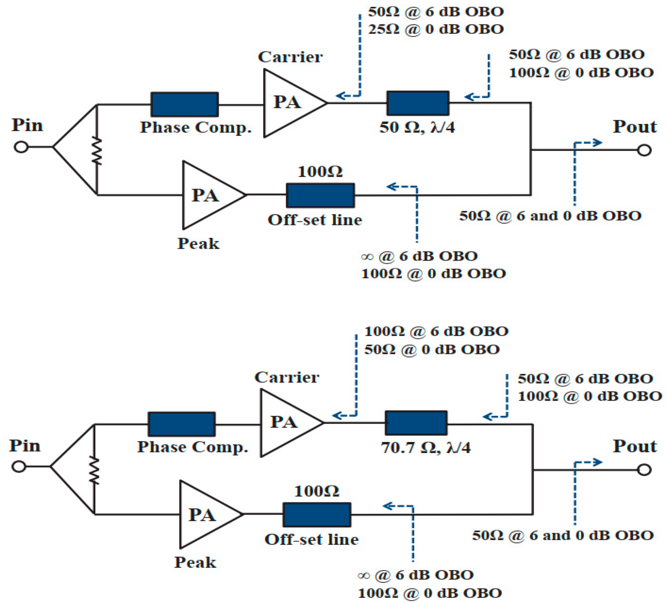
Moreover, a novel dual-band DPA was designed in [31], as shown in Figure 9, where the main concept is to use two quarter-wavelength transmission lines at the output of the auxiliary amplifier and only one at the output of the main amplifier, where the impedances are 70.7 Ω and 50 Ω in the auxiliary output path and 70.7 Ω in the main output path. The main purpose of these additional lines is to improve the broadband performance compared to the traditional DPA, where only one quarter-wavelength line is used at the output of the main amplifier. The improvement was made by reducing the impedance transformation ratio, as shown in the following equations, so that the loaded Q factor will be reduced to increase the band covered. In the classical DPA, the impedance transformation ratio is 1:4 to transfer 25 Ω to 100 Ω so that the loaded Q factor will be:
Q L = 100 Ω 25 Ω 1 = 1.73
whereas, in the design of [31], the impedance ratio is 1:2 making the loaded Q factor equal to 1:
Q L = 100 Ω 50 Ω 1 = 1
Hence, there is an increment of 1.73 times in terms of frequency bandwidth. At the back-off region, the main amplifier will see 100 Ω due to using the 70.7 Ω quarter wavelength line, whereas both amplifiers would see a 50 Ω at the saturation point.
Besides, a dual-band Doherty amplifier design using class-J amplifier was studied in [32], where the imperfect high impedance seen towards the peaking amplifier at the back-off region was utilized to be part of the output matching of the main amplifier at the fundamental frequency matching. Whereas the control of harmonics was carried out using a post matching network after examining the load pull data of the main amplifier to determine the location of the second harmonic.
Shao et al. [19] modified the structure of a DPA so that they eliminated the effect of the impedance inverter at the output of classical DPA, and in addition used four transmission line sections (two in series and two in shunt), as shown in Figure 10, in order to make the proposed DPA works in dual-band according to the equations proposed by Chuang [33]. They suggested matching the main amplifier to 50 Ω and the auxiliary amplifier to 100 Ω. In this case, at low input power, the main and auxiliary amplifiers will see 50 Ω and ∞ Ω respectively, whereas at the high-power region, they will see 25 Ω and 100 Ω respectively. Two simplified designs for dual-Band DPA were done by [34], where the designs were tested, the main advantage of these new structures is the impedance inverter at the output power of DPA is eliminated as shown in Figure 11 [34]. This was done by changing matching the auxiliary output impedance to 100 Ω instead of 50 Ω. In this case, only one quarter-wavelength impedance inverter will be needed at the output.
Monolithic microwave integrated circuit (MMIC) was used to design dual-band Doherty amplifier [14,35,36,37], because the power ratio between the main and the auxiliary amplifier which determines the back-off of the DPA depends on the availability of devices in the market; however, this can be ignored when MMIC technology is used. The linearity of the DPA was improved in [35] by cancelling the effects of the third-order intermodulation (IM3) by using a tunable capacitor at the input to make sure that the phase difference between IM3 of the main amplifier and IM3 of the auxiliary amplifier is equal to 180°, and their IM3 magnitudes are same.
In addition, MMIC dual-band multi-mode power amplifier was designed by [36], where at the lower band (3.5 GHz), the amplifiers work as Doherty amplifier; whereas at the upper band (5.8 GHz) both amplifiers biased as class AB. It should be noted that the load seen by both amplifiers are modified to be Z 0 instead of Z 0 / 2 for the purposing of reducing the transformation ratio. At the same time, high and low pass filters were used at the input side of both the main and peaking amplifier respectively to compensate the phase difference between the amplifiers due to the frequency band change.

3.5. Dual-Band Design Improvements

The linearity of the DPA can be improved by employing the ET technique at the gate of each transistor [38], where the effect of the third order modulation can be cancelled. In addition, varactor diodes have also been used adaptively for improving the bandwidth [39,40]; these techniques have very complex circuity. Moreover, dual-band reconfigurable Doherty amplifier was introduced by [21] where a PIN diode was used adaptively in to remove the reactance components of the load each frequency band. There was an enhancement about 5% of power added efficiency (PAE) compared with a traditional DPA, at the same time, the diode was used to switch between the two bands, where the state of the diode determines the selected band. Moreover, a large back-off compared to previous works been achieved in [23,41,42], which describe a dual-band multiway DPA.
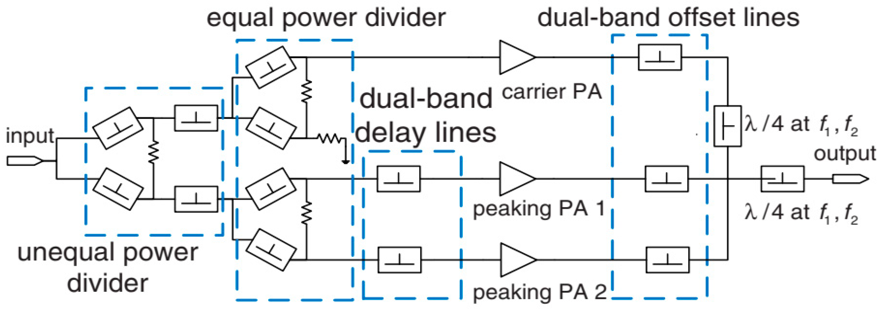
A tri-way DPA was designed to cover the two bands 0.9 GHz and 2.31 GHz using an unequal power divider as shown in Figure 12, where three Wilkinson power dividers are used to produce a quad-way power divider, the first power divider was split the input power unequally, whereas the next two power splitter split the power equally in order to avoid adjusting the auxiliary gate bias by showing the importance of power splitter to manipulate the gain of the auxiliary amplifier that varies depending on the frequency [43]. The saturated designed power was 46 dBm, whereas 61% and 44% efficiency at 9 dB back-off power were achieved at both bands respectively.
It can be noticed that the amount of output current of the auxiliary amplifier is less than for the main amplifier due to the lower gain of the auxiliary amplifier which is deeply biased; in this case, less efficient load-modulation will occur at a high-power level. For this reason, an appropriate selection of the power ratio should be chosen to maximize the load-modulation effects. Depending on the probability density function of a signal with a non-constant envelope, i.e., it has a substantial value of PAPR, the output signal spends most of the time near to the average output power. Hence, the power amplifier should be designed to produce its highest efficiency near the average power.
Adaptive input power control for a dual-band DPA was used in [44], which relied on the adaptive power splitter invented by Nick et al. [45]. The adaptive input can be used to deliver more power to the main amplifier than the auxiliary amplifier when the DPA is working in the low power region and vice versa. The main idea of [45] is to make the auxiliary amplifier turn on later so that, at the OBO, early load modulation can be avoided and after that, more power will be delivered to the auxiliary amplifier to compensate the low gain due to the biasing condition and improving the load modulation.
Extending the bandwidth of a dual-band of DPA using a novel output combiner was realized in [46] where a resonant shunt LC tank was added at the combining node to maintain the main amplifier back-off impedance and reactance compensation by reducing the reactance variation with frequency, however, this technique is limited by the LC band. In the work presented by [46], the 20 W peak power DPA used two GaN HEMT devices with different capabilities, where a 10 W device was used for the main amplifier and operated as class F, whereas a 25 W device was used for the auxiliary amplifier and biased as class C. This amplifier showed a PAE of 42% when the dual-band input contained long term evolution (LTE) and WCDM signals concurrently with 15 MHz bandwidth for each.
In [47,48], the main and auxiliary power amplifiers operating classes was changed to class ABJ, where harmonics control was employed. The main thing to note is the linearity measurements in terms of adjacent channel power ratio (ACPR) were less than 25 dBc for both bands. New technology elements were used in the designs of [49,50], where micro-electro-mechanical switches (MEMS) were used to select the operating dual-band of quarter wave transmission line, where the switches move the operation center frequency from one band to another depending on the state of the switches. This technique depends on the reliability of switches and their load power limitations. At the same time, this technology suffers from slow switching speed and high actuation voltage in addition to temperature sensitivity and dielectric charging problems [51].
In [52], the combiner section was simplified by matching both amplifiers to 70 Ω as illustrated in Figure 13, at the same time, the load impedance was still 50 Ω, in this case, however, a mismatch between the load and the matching networks will be introduced (−15 dB return loss) in the cost of simplifying the combiner. Further work of reconfigurable as well as concurrent dual-band DPAs was described by [53] where the reconfigurability had been achieved by using switches.
The proposed design of digital DPA in [17] targeting 850 MHz and 1.7 GHz bands depends on a 3-coil current-mode combiner which is used as a power combiner of 4-way. The transformer is maintained to reduce the ground parasitic and minimize the mismatch between the two PAs. At the peaking power, both PAs are working, and the currents at the two primary coils are in-phase so that the impedance seen by each amplifier is 50 Ω. However, the load impedance seen by each PA stays the same when the output power is backed off if the two PAs are controlled synchronously, so that, in [17], both amplifiers are controlled independently in order to perform load modulation. At the same time, a switched capacitor is used because of its good performance in terms of linearity and efficiency. Another attempt targeting mm-wave was done by [54]. A simulation and detailed passive design are discussed in this paper for mm-wave: the lower band was 24 GHz and the upper bad was 28 GHz with a bandwidth of 1 GHz.
A recent work using digital dual-input power was done by [55] targeting a dual-band Doherty power amplifier, where the difference of the reactance impedance that the transistor needs to see at the input side for both bands is eliminated by using a short-circuited shunt stub. Moreover, the load modulation of the designed circuit was improved by using different drain voltages, where 22 V and 36 V were used for both the main and the auxiliary amplifier, the difference in drain voltages helped the main amplifier to be more efficient at the back-off and more current to be got from the auxiliary amplifier, where the load modulation can be improved.

3.6. Tri-Band and Quad-Band DPA

In addition to the dual-band DPA, there are researches which focus on tri- and quad-band DPA [56,57,58,59,60]. A design approach was used in [58] to cover three frequency bands. In the design, it was taking into considerations that all sections of the DPA should be able to give good performance at each band. However, the implemented design showed a relative shift in the band center frequencies.
A tri-band DPA targeting three types of mobile applications—LTE, universal mobile telecommunications service (UMTS), and WiMAX—was studied in [60], where two-stage DPA was designed for an average output power of 35 dBm. The results in [60] showed a good scattering parameters response. At the input side of the designed power amplifier, a broadband divider was used to cover the selected frequency bands, on the other hand, the impedance inverter network and the impedance transforming network were designed to fulfil the requirements of the tri-band. The designed PA was fabricated and tested using 10 MHz LTE for the lower frequency band, and two carriers with a WCDMA signal of 10 MHz for the upper bands. Each testing signal is used individually for the design evaluation.
The work of [58] has been extended in [56] to cover quad-band instead of tri-band operation. The chosen bands were 0.9 GHz, 1.5 GHz, 2.1 GHz and 2.6 GHz. Two transistors were used to implement asymmetrical DPA: these transistors are 10 W and 25 W with different power supplies for the main and the carrier. Although asymmetrical DPA was used, the authors in [56] were looking for only 6 dB OBO. The most complicated part in multiband DPA is the multiband impedance inverter network which should give good impedance inversion over the selected bands so that, in [56], at the input side, a wideband Wilkinson power divider was used to cover the four bands.
Proof of multi-band Doherty was presented by [61], where three boards were designed targeting three bands; the boards were identical in terms of the artwork, however for each band different capacitors and resistors were used. The work of [61] can be improved by using digitally controlled switches so that one reconfigurable board can be used for the three bands. In [62], a 3-way Doherty power amplifier targeting 1.8–2.2 GHz frequency bands suitable for mobile base-stations was achieved depending on LDMOS RFIC technology, a 47% efficiency accomplished at 12 dB back-off.

3.7. Linearization of Dual-Band DPA

Finally, power amplifiers in general often need to be linearized, especially when they operates at the nonlinear region to avoid interfering with the next adjacent channel. This can be achieved, for example, by using digital pre-distortion (DPD) which is widely renowned in its ability to improve the linearity performance of the designed dual-band due to its reconfigurable capability, accuracy, and its implementation in the digital domain. Using DPD will improve the signal linearity; however, the system complexity will be increased, as there has to be an additional circuit added to the system [63]. However, there is a deterioration in the performance of concurrent dual-band power amplifiers since it is not easy for the DPD to correct the signal at two different frequency bands at the same time. This is obvious because the nonlinearity behavior of the power amplifier is different from one frequency band to another. A possible solution is to use a new technique called two-dimensional digital predistortion (2D-DPD), which, though more complex than ordinary DPD, can deal will dual-band PA [30]. At the same time, the crest factor also leads to performance degradation in dual-band PA. A two-dimensional crest factor reduction was studied and used in [30] to improve the linearity. Table 2 shows a comparison of performance achieved in dual-band DPA in addition to the signal test type that was used in each work; it can be noticed that most of the works were done using GaN HEMT.

4. Conclusions

The techniques for designing dual-band Doherty amplifier have been reviewed and presented. The main limitation of each technique has been also addressed. The dual-band DPA was found as a promising technique that can be used in modern and future communications systems (e.g., satellite communications and mobile communications) where carrier aggregation and SDR can be applied. It was concluded that the offset line length mainly depends on the parasitic effect of the amplifier, in addition to the matching network characteristics. Using modern RF switches, which may include MEMS, can help to make the design of dual-band power amplifiers easier. The linearization process depends on characteristics of the PA devices, which vary depending on the operational frequency band, so that, in multi-band power amplifiers, the linearization process will be more complex and may be extremely so when the frequency bands are used concurrently. A solution for dual-band linearization is to use 2D-DPD, which will be able to achieve the required linearity at the cost of complexity. The DPA back-off depends mainly on the load modulation between the main and auxiliary amplifier, and at the same time, can be increased as the power ratio between the peaking power and the main power increases; however, selecting device sizes for the main and the auxiliary amplifiers is not always easy because it depends on the market availability of the devices. The use of MMIC technology gives flexibility in selecting the device peak power ratio; nevertheless, the output power of this technology is still low. For low frequency up to 2.2 GHz, LDMOSFET technology is often preferable; however, the GaN HEMT has smaller input and output capacitance due to its small periphery, and its transition frequency is high. Currently, the GaN HEMT has a good broadband performance, high efficiency, and large breakdown voltage, due to its features. It has given the designers a better ability to design an efficient PA.
The market for mobile communications covering more than one frequency band is growing. In this frame, the dual-band or multi-band Doherty amplifier can support the operation of the PA to cover two or more frequency bands with good efficiency at the back-off power, for which, the cost and the size can be reduced at the same time to preserve energy efficient operation.

Author Contributions

Conceptualization, A.M.A. and M.A.Y.; Methodology, A.M.A., N.M. and M.A.Y.; Software, A.M.A., R.A.A.-A. and M.A.Y.; Validation, A.M.A., R.A.A.-A., N.M. and A.R.; Formal analysis, A.M.A., R.A.A.-A., J.N., N.M., N.O.P., Y.I.A.A.-Y. and A.R.; Investigation, A.M.A., M.A.Y., R.A.A.-A., J.N., N.M., N.O.P., Y.I.A.A.-Y. and A.R.; Resources, A.M.A., M.A.Y., R.A.A.-A., J.N. and Y.I.A.A.-Y.; Data curation, A.M.A., M.A.Y. and R.A.A.-A.; Writing—original draft preparation, A.M.A., M.A.Y. and R.A.A.-A.; Writing—review and editing, A.M.A., M.A.Y., J.N. and R.A.A.-A.; Visualization, A.M.A., M.A.Y., R.A.A.-A. and J.N.

Funding

This project has received funding from the European Union’s Horizon 2020 research and innovation programme under grant agreement H2020-MSCA-ITN-2016 SECRET-722424.

Acknowledgments

Authors wish to express their thanks for the support provided by the innovation programme under grant agreement H2020-MSCA-ITN-2016 SECRET-722424.

Conflicts of Interest

The authors declare no conflict of interest.

References

  1. Cripps, S.C. RF Power Amplifiers for Wireless Communications; Artech House: Norwood, MA, USA, 2006. [Google Scholar]
  2. Kerhervé, E.; Belot, D. Linearization and Efficiency Enhancement Techniques for Silicon Power Amplifiers: From RF to mmW; Elsevier Science: New York, NY, USA, 2015. [Google Scholar]
  3. Colantonio, P.; Giannini, F.; Limiti, E. High Efficiency RF and Microwave Solid State Power Amplifiers; John Wiley & Sons Ltd.: West Suss, UK, 2009. [Google Scholar]
  4. Camarchia, V.; Pirola, M.; Quaglia, R.; Jee, S.; Cho, Y.; Kim, B. The Doherty Power Amplifier: Review of Recent Solutions and Trends. IEEE Trans. Microw. Theory Tech. 2015, 63, 559–571. [Google Scholar] [CrossRef] [Green Version]
  5. Doherty, W.H. A new high-efficiency power amplifier for modulated waves. Bell Syst. Tech. J. 1936, 15, 469–475. [Google Scholar] [CrossRef]
  6. Kim, H.; Seo, C. Improvement of Power Added Efficiency and Linearity in Doherty Amplifier using Dual Bias Control and Photonic Band-Gap Structure. In Proceedings of the 2007 Asia-Pacific Microwave Conference, Bangkok, Thailand, 11–14 December 2007; pp. 1–4. [Google Scholar]
  7. Li, X.; Chen, W.; Zhang, Z.; Feng, Z.; Tang, X.; Mouthaan, K. A concurrent dual-band doherty power amplifier. In Proceedings of the 2010 Asia-Pacific Microwave Conference, Yokohama, Japan, 7–10 December 2010; pp. 654–657. [Google Scholar]
  8. Saad, P.; Piazzon, L.; Colantonio, P.; Moon, J.; Giannini, F.; Andersson, K.; Kim, B.; Fager, C. Multi-band/multi-mode and efficient transmitter based on a Doherty Power Amplifier. In Proceedings of the 2012 42nd European Microwave Conference, Amsterdam, The Netherlands, 29 October–1 November 2012; pp. 1031–1034. [Google Scholar]
  9. Gustafsson, D.; Andersson, C.M.; Fager, C. A Modified Doherty Power Amplifier With Extended Bandwidth and Reconfigurable Efficiency. IEEE Trans. Microw. Theory Tech. 2013, 61, 533–542. [Google Scholar] [CrossRef]
  10. Barakat, A.; Thian, M.; Fusco, V.; Bulja, S.; Guan, L. Toward a More Generalized Doherty Power Amplifier Design for Broadband Operation. IEEE Trans. Microw. Theory Tech. 2017, 65, 846–859. [Google Scholar] [CrossRef]
  11. Lin, J.; Xie, Z. Analysis and Design of a High Efficient Dual-Frequency Doherty Power Amplifier. In Proceedings of the 2018 International Conference on Microwave and Millimeter Wave Technology (ICMMT), Chengdu, China, 7–11 May 2018; pp. 1–3. [Google Scholar]
  12. Chen, X.; Chen, W.; Huang, F.; Ghannouchi, F.M.; Feng, Z.; Liu, Y. Systematic Crest Factor Reduction and Efficiency Enhancement of Dual-Band Power Amplifier Based Transmitters. IEEE Trans. Broadcast. 2017, 63, 111–122. [Google Scholar] [CrossRef]
  13. Kelly, N.; Cao, W.; Zhu, A. Preparing Linearity and Efficiency for 5G: Digital Predistortion for Dual-Band Doherty Power Amplifiers with Mixed-Mode Carrier Aggregation. IEEE Microw. Mag. 2017, 18, 76–84. [Google Scholar] [CrossRef]
  14. Chen, W.; Chen, X.; Zhang, S.; Feng, Z. Energy-efficient concurrent dual-band transmitter for multistandard wireless communications. In Proceedings of the 2014 Asia-Pacific Microwave Conference, Sendai, Japan, 4–7 November 2014; pp. 558–560. [Google Scholar]
  15. Chen, X.; Chen, W.; Gongzhe, S.; Ghannouchi, F.M.; Feng, Z. A concurrent dual-band 1.9–2.6-GHz Doherty power amplifier with Intermodulation impedance tuning. In Proceedings of the 2014 IEEE MTT-S International Microwave Symposium (IMS2014), Tampa, FL, USA, 1–6 June 2014; pp. 1–4. [Google Scholar]
  16. GSMA. 5G Spectrum GSMA Public Policy Position. Available online: https://www.gsma.com/latinamerica/5g-spectrum-gsma-public-policy-position/ (accessed on 15 February 2019).
  17. Yin, Y.; Xiong, L.; Zhu, Y.; Chen, B.; Min, H.; Xu, H. A compact dual-band digital doherty power amplifier using parallel-combining transformer for cellular NB-IoT applications. In Proceedings of the 2018 IEEE International Solid-State Circuits Conference (ISSCC), San Francisco, CA, USA, 11–15 February 2018; pp. 408–410. [Google Scholar]
  18. Liu, M.; Golestaneh, H.; Boumaiza, S. A concurrent 2.15/3.4 GHz dual-band Doherty power amplifier with extended fractional bandwidth. In Proceedings of the 2016 IEEE MTT-S International Microwave Symposium (IMS), San Francisco, CA, USA, 22–27 May 2016; pp. 1–3. [Google Scholar]
  19. Shao, J.; Poe, D.; Ren, H.; Arigong, B.; Zhou, M.; Ding, J.; Zhou, R.; Kim, H.S.; Zhang, H. Dual-band microwave power amplifier design using GaN transistors. In Proceedings of the 2014 IEEE 57th International Midwest Symposium on Circuits and Systems (MWSCAS), College Station, TX, USA, 3–6 August 2014; pp. 559–562. [Google Scholar]
  20. Ghannouchi, F.M.; Rawat, K. Doherty power amplifiers in software radio systems. In Proceedings of the 2011 XXXth URSI General Assembly and Scientific Symposium, Istanbul, Turkey, 13–20 August 2011; pp. 1–4. [Google Scholar]
  21. Park, J.; Yook, J.; Kim, Y.; Lee, C.H. Dual-band switching Doherty power amplifier using phase shifter composed of PIN diode. In Proceedings of the 2011 6th European Microwave Integrated Circuit Conference, Manchester, UK, 10–11 October 2011; pp. 300–303. [Google Scholar]
  22. Bathich, K.; Gruner, D.; Boeck, G. Analysis and design of dual-band GaN HEMT based Doherty amplifier. In Proceedings of the 2011 6th European Microwave Integrated Circuit Conference, Manchester, UK, 10–11 October 2011; pp. 248–251. [Google Scholar]
  23. Xiang, L.; Wenhua, C.; Zisheng, L.; Zhenghe, F.; Yaqin, C.; Ghannouchi, F.M. Design of dual-band multi-way Doherty power amplifiers. In Proceedings of the 2012 IEEE/MTT-S International Microwave Symposium Digest, Montreal, QC, Canada, 17–22 June 2012; pp. 1–3. [Google Scholar]
  24. Vizmuller, P. RF Design Guide: Systems, Circuits, and Equations; Artech House: Norwood, MA, USA, 1995. [Google Scholar]
  25. Saad, P.; Colantonio, P.; Piazzon, L.; Giannini, F.; Andersson, K.; Fager, C. Design of a Concurrent Dual-Band 1.8–2.4-GHz GaN-HEMT Doherty Power Amplifier. IEEE Trans. Microw. Theory Tech. 2012, 60, 1840–1949. [Google Scholar] [CrossRef]
  26. Wang, G.; Zhao, L.; Szymanowski, M. A Doherty amplifier for TD-SCDMA base station applications based on a single packaged dual-path integrated LDMOS power transistor. In Proceedings of the 2010 IEEE MTT-S International Microwave Symposium, Anaheim, CA, USA, 23–28 May 2010; pp. 1512–1515. [Google Scholar]
  27. Abdulkhaleq, A.M.; Al-Yasir, Y.; Ojaroudi Parchin, N.; Brunning, J.; McEwan, N.; Rayit, A.; Abd-Alhameed, R.A.; Noras, J.; Abduljabbar, N. A 70-W Asymmetrical Doherty Power Amplifier for 5G Base Stations. In Proceedings of the Broadband Communications, Networks, and Systems, Faro, Portugal, 19–20 September 2018; pp. 446–454. [Google Scholar]
  28. Monzon, C. A small dual-frequency transformer in two sections. IEEE Trans. Microw. Theory Tech. 2003, 51, 1157–1161. [Google Scholar] [CrossRef]
  29. Colantonio, P.; Feudo, F.; Giannini, F.; Giofrè, R.; Piazzon, L. Design of a dual-band GaN Doherty amplifier. In Proceedings of the 18th International Conference on Microwaves, Radar and Wireless Communications, Vilnius, Lithuania, 14–16 June 2010; pp. 1–4. [Google Scholar]
  30. Chen, W.; Chen, X.; Zhang, S.; Feng, Z. Energy-efficient power amplifier techniques for TD-SCDMA and TD-LTE multi-standard wireless communications. In Proceedings of the 2014 XXXIth URSI General Assembly and Scientific Symposium (URSI GASS), Beijing, China, 16–23 August 2014; pp. 1–4. [Google Scholar]
  31. Grebennikov, A.; Wong, J. A Dual-Band Parallel Doherty Power Amplifier for Wireless Applications. IEEE Trans. Microw. Theory Tech. 2012, 60, 3214–3222. [Google Scholar] [CrossRef]
  32. Yang, Z.; Li, M.; Yao, Y.; Dai, Z.; Li, T.; Jin, Y. Design of Concurrent Dual-Band Continuous Class-J Mode Doherty Power Amplifier With Precise Impedance Terminations. IEEE Microw. Wirel. Compon. Lett. 2019, 29, 348–350. [Google Scholar] [CrossRef]
  33. Chuang, M. Dual-Band Impedance Transformer Using Two-Section Shunt Stubs. IEEE Trans. Microw. Theory Tech. 2010, 58, 1257–1263. [Google Scholar] [CrossRef]
  34. Ren, H.; Shao, J.; Arigong, B.; Zhou, M.; Fu, S.; Ding, J.; Kim, H.; Zhang, H. Simplified Doherty power amplifier structures. In Proceedings of the 2015 Texas Symposium on Wireless and Microwave Circuits and Systems (WMCS), Waco, TX, USA, 23–24 April 2015; pp. 1–3. [Google Scholar]
  35. Jee, S.; Yunsik, P.; Cho, Y.; Lee, J.; Seokhyeon, K.; Bumman, K. A highly linear dual-band Doherty power amplifier for femto-cell base stations. In Proceedings of the 2015 IEEE MTT-S International Microwave Symposium, Phoenix, AZ, USA, 17–22 May 2015; pp. 1–4. [Google Scholar]
  36. Lv, G.; Chen, W.; Liu, X.; Feng, Z. A Dual-Band GaN MMIC Power Amplifier With Hybrid Operating Modes for 5G Application. IEEE Microw. Wirel. Compon. Lett. 2019, 29, 228–230. [Google Scholar] [CrossRef]
  37. Lv, G.; Chen, W.; Chen, X.; Ghannouchi, F.M.; Feng, Z. A Compact Ka/Q Dual-Band GaAs MMIC Doherty Power Amplifier With Simplified Offset Lines for 5G Applications. IEEE Trans. Microw. Theory Tech. 2019, 1–12. [Google Scholar] [CrossRef]
  38. Moon, J.; Kim, J.; Kim, I.; Kim, B. A Wideband Envelope Tracking Doherty Amplifier for WiMAX Systems. IEEE Microw. Wirel. Compon. Lett. 2008, 18, 49–51. [Google Scholar] [CrossRef]
  39. Qureshi, J.H.; Nan, L.; Neo, E.; Rijs, F.V.; Blednov, I.; de Vreede, L. A wide-band 20W LDMOS Doherty power amplifier. In Proceedings of the 2010 IEEE MTT-S International Microwave Symposium, Anaheim, CA, USA, 23–28 May 2010; p. 1. [Google Scholar]
  40. Sarkeshi, M.; Leong, O.B.; van Roermund, A. A novel Doherty amplifier for enhanced load modulation and higher bandwidth. In Proceedings of the 2008 IEEE MTT-S International Microwave Symposium Digest, Atlanta, GA, USA, 15–20 June 2008; pp. 763–766. [Google Scholar]
  41. Barthwal, A.; Ajmera, G.; Rawat, K.; Basu, A.; Koul, S.K. Design scheme for dual-band three stage Doherty Power Amplifiers. In Proceedings of the 2014 IEEE International Microwave and RF Conference (IMaRC), Bangalore, India, 15–17 December 2014; pp. 80–83. [Google Scholar]
  42. Liu, M.; Fang, X.; Huang, H.; Boumaiza, S. Dual-band 3-way Doherty Power Amplifier with Extended Back-off Power and Bandwidth. IEEE Trans. Circuits Syst. II Express Briefs 2019, 1. [Google Scholar] [CrossRef]
  43. Li, X.; Chen, W.; Feng, Z.; Ghannouchi, F.M. Design of dual-band tri-way GaN doherty power amplifier with frequency dependent power division. Electron. Lett. 2012, 48, 797–798. [Google Scholar] [CrossRef]
  44. Chen, W.; Zhang, S.; Liu, Y.; Ghannouchi, F.M. A Concurrent Dual-Band Uneven Doherty Power Amplifier with Frequency-Dependent Input Power Division. IEEE Trans. Circuits Syst. I Regul. Pap. 2014, 61, 552–561. [Google Scholar] [CrossRef]
  45. Nick, M.; Mortazawi, A. Adaptive Input-Power Distribution in Doherty Power Amplifiers for Linearity and Efficiency Enhancement. IEEE Trans. Microw. Theory Tech. 2010, 58, 2764–2771. [Google Scholar] [CrossRef]
  46. Abadi, M.N.A.; Golestaneh, H.; Sarbishaei, H.; Boumaiza, S. An extended bandwidth Doherty power amplifier using a novel output combiner. In Proceedings of the 2014 IEEE MTT-S International Microwave Symposium (IMS2014), Tampa, FL, USA, 1–6 June 2014; pp. 1–4. [Google Scholar]
  47. Carrubba, V.; Ture, E.; Maroldt, S.; Mußer, M.; Raay, F.V.; Quay, R.; Ambacher, O. A dual-band UMTS/LTE highly power-efficient Class-ABJ Doherty GaN PA. In Proceedings of the 2015 European Microwave Conference (EuMC), Paris, France, 7–10 September 2015; pp. 1164–1167. [Google Scholar]
  48. Carrubba, V.; Ture, E.; Maroldt, S.; Mußer, M.; Raay, F.V.; Quay, R.; Ambacher, O. A dual-band UMTS/LTE highly power-efficient class-ABJ Doherty GaN PA. In Proceedings of the 2015 10th European Microwave Integrated Circuits Conference (EuMIC), Paris, France, 7–8 September 2015; pp. 313–316. [Google Scholar]
  49. Kalyan, R.; Rawat, K.; Koul, S.K. Design of reconfigurable concurrent dual-band quarter-wave transformer with application of power combiner/divider. In Proceedings of the 2015 IEEE MTT-S International Microwave and RF Conference (IMaRC), Hyderabad, India, 10–12 December 2015; pp. 169–172. [Google Scholar]
  50. Kalyan, R.; Rawat, K.; Koul, S.K. Design of reconfigurable concurrent dual-band power amplifiers using reconfigurable concurrent dual-band matching network. In Proceedings of the 2016 IEEE MTT-S International Wireless Symposium (IWS), Shanghai, China, 14–16 March 2016; pp. 1–4. [Google Scholar]
  51. Lahiri, S.K.; Saha, H.; Kundu, A. RF MEMS SWITCH: An overview at- a-glance. In Proceedings of the 2009 4th International Conference on Computers and Devices for Communication (CODEC), Kolkata, India, 14–16 December 2009; pp. 1–5. [Google Scholar]
  52. Fan, M.; Yu, C.; Yu, Q.; Liu, Y. Design of a dual-band Doherty power amplifier utilizing improved combiner. In Proceedings of the 2016 IEEE International Conference on Computational Electromagnetics (ICCEM), Guangzhou, China, 23–25 February 2016; pp. 313–315. [Google Scholar]
  53. Kalyan, R.; Rawat, K.; Koul, S.K. Reconfigurable and Concurrent Dual-Band Doherty Power Amplifier for Multiband and Multistandard Applications. IEEE Trans. Microw. Theory Tech. 2017, 65, 198–208. [Google Scholar] [CrossRef]
  54. Taghian, F.; Abdipour, A.; Mohammadi, A.; Roodaki, P.M. Design and nonlinear analysis of a dual-band Doherty power amplifier for ISM and LMDS applications. In Proceedings of the 2011 IEEE Applied Electromagnetics Conference (AEMC), Kolkata, India, 18–22 December 2011; pp. 1–4. [Google Scholar]
  55. Kalyan, R.; Rawat, K.; Koul, S.K. A Digitally Assisted Dual-Input Dual-Band Doherty Power Amplifier With Enhanced Efficiency and Linearity. IEEE Trans. Circuits Syst. II Express Briefs 2019, 66, 297–301. [Google Scholar] [CrossRef]
  56. Nghiem, X.A.; Negra, R. Design of a concurrent quad-band GaN-HEMT Doherty power amplifier for wireless applications. In Proceedings of the 2013 IEEE MTT-S International Microwave Symposium Digest (MTT), Seattle, WA, USA, 2–7 June 2013; pp. 1–4. [Google Scholar]
  57. Li, X.; Helaoui, M.; Ghannouchi, F.; Chen, W. A Quad-Band Doherty Power Amplifier Based on T-Section Coupled Lines. IEEE Microw. Wirel. Compon. Lett. 2016, 26, 437–439. [Google Scholar] [CrossRef]
  58. Nghiem, X.A.; Negra, R. Novel design of a concurrent tri-band GaN-HEMT Doherty power amplifier. In Proceedings of the 2012 Asia Pacific Microwave Conference Proceedings, Kaohsiung, Taiwan, 4–7 December 2012; pp. 364–366. [Google Scholar]
  59. Rawat, K.; Gowrish, B.; Ajmera, G.; Kalyan, R.; Basu, A.; Koul, S.; Ghannouchi, F.M. Design strategy for tri-band Doherty power amplifier. In Proceedings of the WAMICON 2014, Tampa, FL, USA, 6 June 2014; pp. 1–3. [Google Scholar]
  60. Giofré, R.; Costanzo, F.; Vikraman, D.N.M.; Colantonio, P.; Giannini, F. Designing a tri-band concurrent Doherty power amplifier. In Proceedings of the 2015 Integrated Nonlinear Microwave and Millimetre-wave Circuits Workshop (INMMiC), Taormina, Italy, 1–2 October 2015; pp. 1–3. [Google Scholar]
  61. Yanduru, N.K.; Jeckeln, E.; Monroe, R.; Brobston, M. 50W GaN based multi-band Doherty amplifier proof of concept for LTE with 48% efficiency. In Proceedings of the WAMICON 2014, Tampa, FL, USA, 6 June 2014; pp. 1–3. [Google Scholar]
  62. Blednov, I. Wideband 3 way Doherty RFIC with 12 dB back-off power range. In Proceedings of the 2016 11th European Microwave Integrated Circuits Conference (EuMIC), London, UK, 3–4 October 2016; pp. 17–20. [Google Scholar]
  63. Rawat, K.; Ghannouchi, F.M. Design Methodology for Dual-Band Doherty Power Amplifier with Performance Enhancement Using Dual-Band Offset Lines. IEEE Trans. Ind. Electron. 2012, 59, 4831–4842. [Google Scholar] [CrossRef]
  64. Chen, W.; Bassam, S.A.; Li, X.; Liu, Y.; Rawat, K.; Helaoui, M.; Ghannouchi, F.M.; Feng, Z. Design and Linearization of Concurrent Dual-Band Doherty Power Amplifier With Frequency-Dependent Power Ranges. IEEE Trans. Microw. Theory Tech. 2011, 59, 2537–2546. [Google Scholar] [CrossRef]
  65. Pang, J.; He, S.; Dai, Z.; Huang, C.; Peng, J.; You, F. Novel design of highly-efficient concurrent dual-band GaN Doherty power amplifier using direct-matching impedance transformers. In Proceedings of the 2016 IEEE MTT-S International Microwave Symposium (IMS), San Francisco, CA, USA, 22–27 May 2016; pp. 1–4. [Google Scholar]
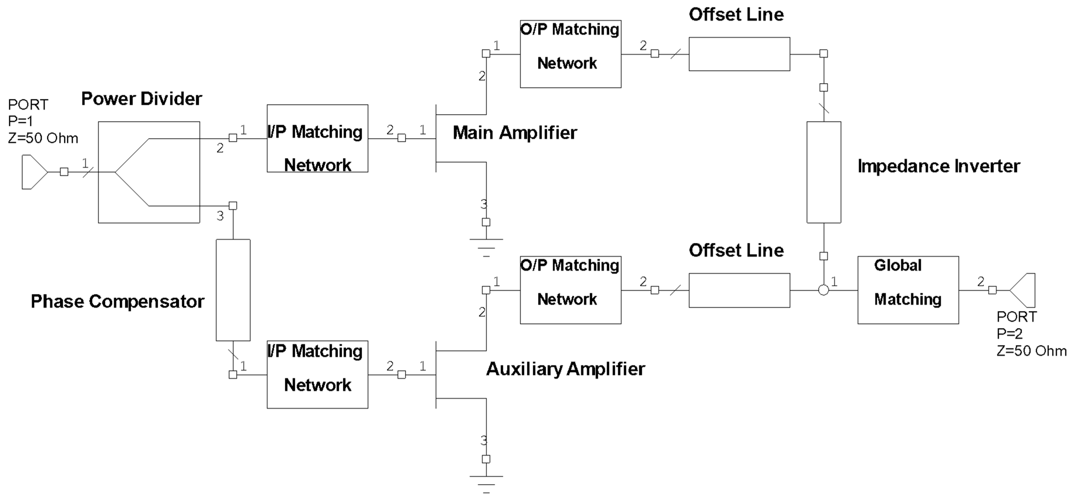
Figure 1. Structure of the Doherty power amplifier.
Electronics 08 00638 g001
Figure 2. Main amplifier load line.
Electronics 08 00638 g002
Figure 3. Doherty equivalent circuit diagram (a) at low power region and (b) at medium and high-power region.
Electronics 08 00638 g003
Figure 4. Voltage and current behavior of Doherty amplifier [10].
Electronics 08 00638 g004
Figure 5. Dual-band global matching network.
Electronics 08 00638 g005
Figure 6. Dual-band Doherty power amplifier (DPA) schematic designed by [25].
Electronics 08 00638 g006
Figure 7. Dual-band DPA schematic [7].
Electronics 08 00638 g007
Figure 8. Schematic dual-band circuit proposed by [18].
Electronics 08 00638 g008
Figure 9. Modified Doherty amplifier proposed by [31].
Electronics 08 00638 g009
Figure 10. Dual-band matching structure used in [19].
Electronics 08 00638 g010
Figure 11. Simplified structure of DPA [34].
Electronics 08 00638 g011
Figure 12. Tri-way Dual-band DPA with frequency dependent power division [43].
Electronics 08 00638 g012
Figure 13. Load modulation proposed by [52].
Electronics 08 00638 g013
Table 1. Phase delay introduced by T- and Π-networks [29].
-Dual-BandSingle Band
T-TopologyΠ-TopologyBoth
S 21 Phase @ f 1 −90°−90°90°
S 21 Phase @ f 2 +90°−90°
Table 2. Samples of achieved dual-band DPA.
ReferenceLower BandUpper BandTest
Frequency (GHz)PPeak (dBm)Efficiency @ PPeak %Back-Off dBEfficiency @OBO %Frequency (GHz)PPeak (dBm)Efficiency @ PPeak %Back-Off dBEfficiency @OBO %Signal TypeSignal Bandwidth
[17]0.8528.936.8 *629.91.72725.4 *616.8 *12-subcarrier NB-IoT/64-QAM/256-QAM WLAN12 * 180k / 20 MHz
[18]2.1547.3NA6523.447NA651WCDMA/LTE20 MHz
[25]1.84364 *660 *2.44354 *644CW/WCDMA/LTE− / 10 MHz
[7]0.941.9NA539.8241.2NA541.4CW-
[29]2.1439506453.5NANANANACW-
[64]0.884140 *633 *1.964038 *630 *CW-
[22]242NA6492.7242NA644CW/WCDMA/LTE− / 5 MHz
[21]2.150NA647 *2.250NA647 *CW/WCDMA− / 5 MHz
[43]0.946669652.154656946CW-
[23]0.9241.5NA733 *1.9941NA829 *CW-
[31]2.1445.5NA6.5452.65545.5NA6.540WCDMA5 MHz
[44]0.854347.5 *645 *2.3342.532 *641 *CW/LTE1/LTE2− / 10 MHz / 15 MHz
[46]0.7543NA9.442 *0.943NA9.472 *CW/WCDMA/LTE− / 15 MHz
[19]0.638.565650140.557637CW-
[41]1.745NA7512.445NA945.5CW/WCDMA/WiMAX−/ 3.84 MHz / 5 MHz
[30]1.936.8NA6.850.12.636.8NA6.850.1LTE1/LTE210 MHz / 15 MHz
[35]2.342.5NA7.230*2.742.5NA7.244.2 *CW/LTE− / 10 MHz
[34]0.64076.3654.9140.254638CW-
[65]1.844726632.64460651CW/LTE− /20 MHz
[52]2.0243.962.1651.12.6344.671.4653.3CW-
[55]0.8544.6589582.144.268968CW-
NA: Not available. CW: Continuous wave. *: Power added efficiency PAE.