Abstract
Content-addressable memory (CAM) is a type of associative memory, which returns the address of a given search input in one clock cycle. Many designs are available to emulate the CAM functionality inside the re-configurable hardware, field-programmable gate arrays (FPGAs), using static random-access memory (SRAM) and flip-flops. FPGA-based CAMs are becoming popular due to the rapid growth in software defined networks (SDNs), which uses CAM for packet classification. Emulated designs of CAM consume much dynamic power owing to a high amount of switching activity and computation involved in finding the address of the search key. In this paper, we present a power and resource efficient binary CAM architecture, Zi-CAM, which consumes less power and uses fewer resources than the available architectures of SRAM-based CAM on FPGAs. Zi-CAM consists of two main blocks. RAM block (RB) is activated when there is a sequence of repeating zeros in the input search word; otherwise, lookup tables (LUT) block (LB) is activated. Zi-CAM is implemented on Xilinx Virtex-6 FPGA for the size 64 × 36 which improved power consumption and hardware cost by 30 and 32%, respectively, compared to the available FPGA-based CAMs.
1. Introduction
Field-programmable gate arrays (FPGAs) are becoming an increasingly favorable platform for systems implementation because of their hardware-like performance and software-like reconfigurability. Modern FPGAs provide a vast amount of configurable logic and embedded memory blocks operating at a high clock rate [1,2]. For example, the 16-nm Xilinx UltraSCALE FPGA and 14-nm Intel Stratix FPGA provide a massive amount of memory and logic resources which can be configured on-the-fly to implement the given functionality. Software defined networks (SDNs) are implemented using FPGAs where flexibility and reconfigurability are the required features for future 5G/SDN networks. Support for packet classification is one of the key element of networking devices, which in most cases are implemented using a content-addressable memory (CAM).
In a CAM, every location is accessed by its content rather than by address which is considered to be similar to the behavior of a human brain [3,4]. Typically, it returns the address of the input search word in one clock cycle. CAM is classified into binary (BCAM) and ternary CAM (TCAM) [5,6]. BCAM stores ‘0’ and ‘1’ while TCAM can store a don’t care bit ‘X’ too. The stored data, in the form of CAM cells, are arranged as rows and columns. The number of rows represents the depth of CAM memory, while the number of columns represents the width of CAM memory. The input search word is compared with each stored word using search lines (SLs) to form the corresponding matchlines (MLs), as shown in Figure 1. The encoder (Enc.) translates MLs into an address where the search key is found. For example, the input search word of value “0101” is matched with the corresponding bits of location 2 to produce a logic-high ML2, which is translated to the address “10” by the encoder as shown in Figure 1.
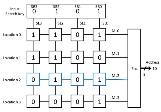
Figure 1.
A 4 × 4 BCAM. (SL0, SL1, SL2, and SL3 are the four search lines; ML0, ML1, ML2, and ML4 are the four matchlines; Enc.: A priority encoder).
Due to high speed searching capability, CAMs have found its place in almost every scientific field where the look-up time is of utmost importance such as pattern recognition [7], security systems, networking applications [8,9], artificial intelligence [10,11]. The efficiency of packet classification and packet forwarding in network routers is tremendously increased by using CAM as its searching memory where look-up time was previously unable to catch the bandwidth of the communication link [12]. FPGAs are used in many applications other than networking. To include a hard core for CAM in FPGA is not a good option for FPGA vendors (such as Xilinx, Altera). Thus, CAMs are emulated using the available hardware resources on FPGAs and are continuously improving in terms of speed, power consumption, and hardware resources.
Conventional CAM (on ASIC) has the drawback of high power consumption, limited storage density, non-scalability, and high implementation cost [3,13], compared with a random-access memory (RAM) which has high storage density and lower power consumption. One CAM cell requires 9–10 transistors, while one RAM cell needs only 6 transistors which makes conventional CAM power inefficient and limits its storage density. Similarly, modern FPGAs do not have a built-in core to support the searching-based applications. Researchers have utilized the RAM blocks (in the form of distributed RAM and block RAM (BRAM)) to emulate the functionality of CAM, such as HP-TCAM, REST [14,15] etc. As the resources on FPGAs are limited, so it needs to be used efficiently in designing complex circuits such as CAM. Thus, a binary CAM design based on distributed memory (LUTRAMs) with lower hardware cost as well as reduced power consumption is proposed and is successfully implemented on FPGA.
BRAMs are large blocks of memory available as 18K and 36K blocks while distributed RAM consists of LUTRAMs which can be configured as 64-bit memory and is beneficial in small size designs. In our proposed design, we use the LUTRAMs and exploit its 6-input structure in modern FPGAs to save power consumption. The input search key is observed for a specific pattern and one of the two different blocks is searched which saves the power consumed by the other block.
The remaining of the paper is arranged as follows: Section 2 discusses the motivations and key contributions of the proposed work. Section 3 provides the prior work on CAM to justify the need for the proposed design. Section 4 elaborates the proposed Zi-CAM architecture, presents an example size CAM architecture, search algorithm, and updating mechanism. Section 5 shows the implementation of Zi-CAM on FPGA and its comparison with other RAM-based CAM architectures. Section 6 concludes this work and discuss the future directions.
2. Motivations and Key Contributions
2.1. Motivations
Packet classification in modern networking architectures, such as SDN and OpenFlow, is implemented using CAM. The incoming packet needs to be redirected to the destination node based on a table maintained by router in the form of CAM. FPGAs are favorable to these networking application due to its re-configurabiltiy and high performance. Several architectures are available in literature to emulate the functionality of CAM using BRAMs [14,15], distributed RAM [16] as well as flip-flops [17,18,19] on FPGAs. The available CAM architectures are power inefficient due to the accessing of complete memory in each search operation. Therefore, a power efficient binary CAM architecture is proposed in the form of Zi-CAM which also shows reduction in hardware resources.
The applications of FPGAs are constantly increasing, specifically, in the field of networking, security, and artificial intelligence [1,19,20], but modern FPGAs lack a soft core for CAM which is an essential element in searching-based applications. Thus, there is a need to develop an optimal CAM core, which can be used for packet classification in modern re-configurable networking systems on FPGAs.
2.2. Key Contributions
Following are the key contributions of the proposed architecture:
- The average power consumption of Zi-CAM for size 64 × 36 is 16.6 mW, which is 30% less than the state-of-the-art BCAM counterparts [14,21]. The dynamic power consumption of [21] is 24 mW.
- The number of static-random access memory (SRAM) cells used by Zi-CAM for 64 × 36 is 208,256, while the available state-of-the-art RAM-based CAM uses 305,856 SRAM cells [21]. Zi-CAM uses 32% fewer SRAM cells than state-of-the-art BCAM counterpart [21,22].
- Unlike Xilinx CAM [16], there are no useless SRAM cells in the Zi-CAM architecture for any size of CAM implementation on FPGA.
- The update latency of the proposed CAM is only 64 clock cycles, compared to the 513 clock cycles of other RAM-based CAM architectures [23,24], which makes it more suitable for practical applications where the data is frequently updated. The update latency of Zi-CAM is independent of the size of CAM while in other RAM-based CAMs, it varies with the size of CAM.
3. Related Works
RAM-based CAMs were initially not implementable on FPGAs due to large resource requirement. The hardware resources required for the architecture presented in patent [25] doubles by increasing the search word by a single bit which becomes impossible to be implemented on FPGA. A search word of size 36 bit requires 64 Gb of RAM and other computational resources is a plus to this requirement. An energy efficient design [26] is also available based on RAM, but it lacks the optimal configuration of the storing patterns.
The CAM memory is partitioned in [14] by mapping CAM bits to different RAM blocks which enabled its implementation on FPGA, but it still suffers from inefficient usage of RAM. UE-TCAM [21] reduced the requirement of RAM blocks and used only half of the memory resources required for HP-TCAM implementation. The hardware utilization as well as power consumption for both binary and ternary CAM implementation of [14] and [21] are almost the same [18] which is why we are comparing its results with Zi-CAM in Table 1. RAM-based CAM architectures [14,15,27,28] are continuously evolving and improving in terms of speed, area, update latency, resources utilization as well as power consumption. We use the same efficient RAM in our implementation but with controlled switching activity and an efficient arrangement of the SRAM cells. With controlled switching activity, 70% to 80% of the hardware is de-activated which results in reduced dynamic power consumption for some input combinations. By using LUTs as memory elements, our proposed architecture uses fewer hardware resources than the available SRAM-based CAM architectures for the same size configuration.

Table 1.
Different Terminologies (Notations).
EE-TCAM [23] select one set of BRAMs in M BRAMs by pre-classifier bits, to achieve memory efficiency compared to other CAM architecture. BRAM-based CAMs including EE-TCAM have higher update latency of at least 512 clock cycles because of the monolithic structure of BRAM [24]. BU-TCAM [29] updates the memory in the form of multiple words and not word by word, but the worst case latency still remains 512 clock cycles for a CAM having 512 locations. On the other hand, our proposed BCAM architecture has update latency of 64 clock cycles independent of the number of words in CAM memory which is discussed in Section 4.5. Similarly, EE-TCAM involves pre-processing of the incoming new words to map it to the SRAM blocks, which is a computational overhead on the whole system. The computational power involved in the pre-processing of the updating stage significantly affect the resultant power consumption where the updates frequency is higher, which is the case in most of the practical applications, i.e., network routers.
Energy consumption at the circuit level [3,30] is reduced by lowering the supply voltage which is an obvious way of power reduction. In our proposed architecture, we are not changing the supply voltage but arrange LUTs in a novel fashion which leads to the controlling of two blocks on the pattern of bits in the search key. Only one block is active at a time and the power required by the other block is saved. Reconfigurability is a major advantage of FPGA-based CAM, which lacks in circuit level implementation of CAM presented in [6].
CAMs that are emulated using block RAMs (BRAMs) [15,31] are efficient only for specific sizes. At some points, an increase of one bit in search word infers a complete BRAM (16k or 32k). For example, Xilinx CAM implements a basic block of CAM (32 × 10) using available BRAM (1024 × 32) and then allows the implementation of 64 × 10, 128 × 10, and so on or 32 × 20, 32 × 30, and so on [16,32]. If we want to implement a CAM of 64 × 36, it uses the resources equal to a 72 × 40 CAM on Virtex-6 FPGA [33] where a lot of SRAM cells are wasted and can not be used somewhere else. In our proposed architecture, one can increase/decrease the depth and width by a single number, and there are no useless SRAM cells. Thus Zi-CAM efficiently utilizes the SRAM cells on FPGAs irrespective of the size configuration of CAM. LUT-based CAM, DURE [34], also utilizes LUTs similar to our proposed BCAM to implement TCAM and provides an update latency of 65 clock cycles.
RAM-based TCAM, REST, is efficient in terms of memory resources and uses only 3 and 25% of HP-TCAM and Z-TCAM resources, respectively [15]. Multiple accesses in REST [15] increase power consumption and the search latency is five clock cycles which is not in favor of the high-speed characteristic of CAM. On the other hand, our proposed architecture is not compromising on the search latency which is the core feature of a CAM and enables high-speed searching operation in only two clock cycles.
Zhuo et al. increased the pipeline stages of RAM-based CAM and accesses the RAM blocks in multiple clock cycles rather than just one clock cycle to achieve the output match address. This increased the search latency up to nine clock cycles when nine stages of distributed RAM are used. Our design in worst case takes two clock cycles search latency. Hash-based CAMs [35] have non-deterministic search latency and the drawback of collision as well as bucket overflow are always part of it. Our proposed architecture provides the match address in a deterministic time of two clock cycles and achieves power efficiency.
4. Proposed Architecture
4.1. Terminology
Table 1 lists the terminologies used in describing the architecture.
4.2. Zi-CAM Architecture
FPGAs have two types of slices: SLICEM and SLICEL. Each slice consists of four LUTs in Xilinx Virtex-6 FPGA. The LUTs inside SLICEM can be used as 64-bit memory, while those in SLICEL can only be used for logic implementation. Zi-CAM is mainly based on LUTs of a SLICEM, which is also called as distributed memory. Zi-CAM consists of two basic blocks; RAM block (RB) and LUTs block (LB). The RB is implemented using distributed RAM or BRAM of the target FPGA. The LB has some combinational circuitry (for logical comparison) and lookup operation (distributed memory in the form of LUTs or LUTRAMs).
Search word (Sw) is divided into two parts during the search operation. One part consists of the most significant bits (MSB) and is represented by M_bits. The second part consists of the least significant bits (LSB) and is named as L_bits. The number of bits in M_bits & L_bits are represented by p & q, with r as the total number of bits in Sw. The division of the proposed CAM design into two blocks, RB and LB, is to search for the Sw in only one block and save the power consumed by another block. In other FPGA-based CAMs [14,27], all of the RAM is accessed to generate the output address. Zi-CAM is accessing only one of the two blocks to search for the input search key, so that the power consumption of the other block can be saved. The concept is illustrated in Figure 2 in which Sw is searched in RB or LB based on the bit pattern in Sw. If RB is searched for the search key, the power consumption of LB is saved and vice versa. Skipping one of the two blocks results in saving the resultant power consumption of the proposed design, which is given in the experimental implementation with FPGA results.
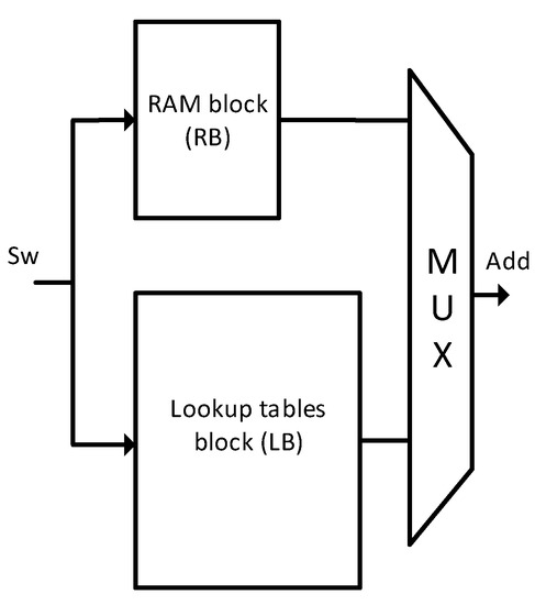
Figure 2.
Dividing of the CAM design in two blocks to save power consumption. (Sw: Search word, Add: Output address where the search word is found).
The two blocks (RB and LB) is activated and deactivated by the output of Block Selector (BSel) which takes L_bits of the search word as input and provides a one-bit signal (named as flag_bit) equal to ‘1’ or ‘0’ as shown in Figure 3. BSel checks for a sequence of zero’s in the search word. If all of the q bits of L_bits are zeros, the flag_bit gets a value of 1 and RB is activated. If at least one bit in L_bits is ‘1’, flag_bit gets a value of ‘0’ and LB is activated. Both RB and LB generates an address, out of which only one is transferred to the output by 2:1 multiplexer (MUX) as shown in Figure 3.
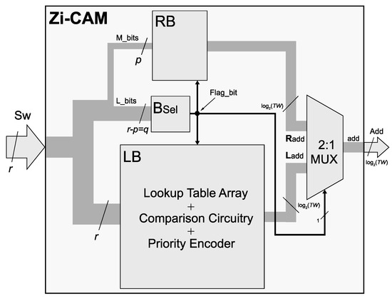
Figure 3.
Zi-CAM Architecture. (LB: lookup tables block, RB: RAM block, BSel: Block Selector, Sw: Input search word, Add: Output address).
RB is a simple SRAM taking M_bits as input, which serves as an address to this memory, and provides Radd at the output. LB is a complex circuit containing LUTs, XNOR gates, ANDing operation, and priority encoder. A 6-input LUT (LUTRAM) has 64 memory cells, starting from 0th cell and end at 63rd cell. The value of M_bits decides the bit location in each LUT. The depth of RB is always 64 in case of 6-input LUTs, because the same 6-inputs are mapped to the input of RB. The width of RB is dependent on the depth of Zi-CAM, for example, the width of RB is 3 bits for eight locations of Zi-CAM. If the number of locations (depth of Zi-CAM) changes to 32, the width of RB becomes 4 bits. Priority encoder is part of LB because the output of LB are matchlines while the output of RB is an address. To provide two similar inputs to the 2:1 MUX, matchlines of LB block should be converted to an address by the priority encoder. The output of RB does not need an encoder as it is already in the form of an address, and not matchlines.
Flag_bit serves as input to three units; RB, LB, and MUX. Algorithm 1 describe the steps in the searching process of Zi-CAM. RB or LB is activated if the value of flag_bit is ‘1’ or ‘0’, respectively. Similarly, the flag_bit is given at the selector input of the MUX. The two inputs to MUX are the address from RB (Radd) and address from LB (Ladd). One of these two addresses (Radd or Ladd) appears at the output of MUX, which is ultimately the address (Add) where the Zi-CAM architecture finds the search word. The number of LUTs used by 8 × 10 are 32, which is the product of LUTs in a row (four LUTs) and the total number of rows (eight rows). The number of inputs to a LUT of the target FPGA decides the value of p. The proposed architecture is mainly evaluated and implemented on Xilinx FPGAs which contain 6-input LUTs in modern devices. Thus, the size of p is 6. Increasing the size of p requires high-input LUTs on target FPGA device. If newer FPGAs are released with 7-input LUTs, the proposed design will perform better. For instance, 8 × 10 Zi-CAM is implemented using 32 6-input LUTs. If 7-input LUTs are available, 8 × 10 Zi-CAM will be implemented using only 24 7-input LUTs.
To simplify the proposed architecture, we explain it with an example size of 8 × 10 binary CAM in a detailed fashion as follows:
| Algorithm 1: Searching Operation in Zi-CAM (Size: 8 × 10) |
| Input: Search word (Sw) Output: Address of the search word in CAM
|
4.3. An Example
An 8 × 10 Zi-CAM consists of one LB (having 32 LUTRAMs, 4-bit AND/NAND gates, and a priority encoder), one RB (RAM of size 64 × 3), a 2:1 MUX and 6-bit AND/NAND gate which acts as BSel. Table 2 shows the content of the CAM that has 10 bits in each of the 8 memory locations (0 to 7). The operation inside LB and RB for 8 × 10 CAM is as follows:
Table 2.
Zi-CAM (8 × 10).
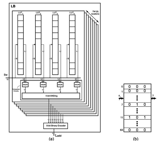
LB: For an 8 × 10 Zi-CAM, LB consists of 8 × 4 = 32 LUTRAMs; four LUTRAMs for each of the eight locations. Four LUTRAMs are arranged in a row and a total of eight rows. The Sw is divided into two parts; one part (6 MSBs) is given as input to every LUTRAM, second part (4 LSBs) is given to the four XNOR gates in such a way that the output of each LUTRAM is compared with one of these four LSBs. The output of four XNOR gates is provided to 4-bit AND gate to create a matchline as shown in Figure 4a. Eight locations create eight mathlines which are provided to the 8:3 encoder to generate 3-bit Ladd.
RB: Only those two words are mapped to RB which has all four LSBs equal to zero; words at 2nd and 5th location of Zi-CAM as shown in Table 1. The six MSBs of these words are given to RB, which is a 64 × 36 RAM as shown in Figure 4b. “010” is stored in the 7th location and “101” is stored in 11th location which is the output address whenever the words stored in 2nd and 5th location of Zi-CAM is given as input search word. Other six words of Table 2 are mapped into LB.
Finally, the 2:1 MUX generates Add by getting Ladd and Radd as two inputs. Flag_bit decides between the Ladd and Radd. If the sw has the continuous sequence of zeros like in 2nd and 7th location in Table 2, Ladd is generated; otherwise Radd. Add is the address where the input search word is found.
4.4. Searching Operation
Algorithm 1 represents the search operation of Zi-CAM from taking the input search word (Sw) to generate the output address (Add). To simplify the whole process, an example size of 8 × 10 is assumed for Zi-CAM in this algorithm. There is only one IF statement which decides the type of block (RB or LB) to be activated for searching the memory. If the sequence of zeroes is found in the input search word, the IF condition (flag_bit == 1) becomes true, and RB is activated. Six MSBs of Sw is provided as input to RB which produces the address (Radd) where the input search word is found.
Sw is forwarded to LB when the IF condition is false. Eight matchlines (M_L[1], M_L[1], …, M_L[7]) are created by comparing the 4 LSBs of Sw with the output of 4 LUTRAMs in each of the eight rows of LUTs. The comparison is shown using XNOR gates in line #7 of Algorithm 1. A priority encoder converts the eight matchlines into Ladd. Line #10 of Algorithm 1 shows the MUX operation which selects one of the two addresses, Ladd and Radd coming from LB and RB, respectively.
4.5. Updating Mechanism
The key component used in Zi-CAM implementation is a LUT, which in Xilinx Virtex-6 FPGA is a 64-bit memory when used from SLICEM slices. In our proposed architecture, each page of LUTRAMs represents a row of CAM as shown in Figure 4a. A page of LUTRAMs is selected on the basis of location where the incoming word needs to be written. In 64 clock cycles, all of the 64-locations in LUTs in the corresponding page is updated by the bit values of the incoming word and a 6-bit counter. The counter’s value act as a 6-bit address to each LUT in the corresponding page. For a TW × r Zi-CAM, the update latency is independent of the size of CAM and can be updated in a constant time of 64 clock cycles because each LUT in modern FPGAs need only 64 clock cycles to be updated completely.
4.6. A Generalized Form
The example in Section 4.3 can be generalized to visualize the larger sizes of Zi-CAM. The increase in depth and width by a single bit infers the appropriate number of LUTRAMs and other FPGA components, unlike other architecture [14,16] which sometimes infer useless circuitry in the form of SRAM cell (BRAMs) as discussed in Section 2.
A TW × r Zi-CAM will infer TW*(r− 6) LUTRAMs for storing of the mapping data with a few additional LUTs for logic implementation. The relationship between the size of Zi-CAM and the hardware cost is linear. Larger the size of Zi-CAM, higher is the hardware cost. The number of XNOR gates are also equal to TW*(r− 6) and the size of priority encoder is TW:(TW). The dimension of RB is 64 ×(TW), if the number of inputs to a single LUT remains constant. In latest FPGAs, the number of inputs to a single LUT remains 6. The MUX needed is always a 2:1 MUX for directing of the two addresses (Radd & Ladd) to the output of Zi-CAM. The size of the bit-vectors coming to MUX is equal to the address of Zi-CAM.
5. Implementation Results
We have successfully implemented the proposed architecture on Xilinx Virtex-6 FPGA [33] device XC6VLX760 using Xilinx ISE Design Suite 14.5. The results are taken using post-route simulations. Xilinx Power Analyzer [36] is used to find the dynamic power consumption for the search input at 100 MHz and 1.0 V core voltage. Energy per bit per search, which is an important metric of comparison for digital systems, is also calculated for Zi-CAM and other counterparts. Comparison of the proposed architecture (Zi-CAM) with other architectures [14,15,16,27] is shown in Table 3.
Table 3.
Comparison with Other Architectures; cc: clock cycles, E/b/s: Energy/bit/search.
The FPGA implementation results shown in Table 3 indicate that Zi-CAM has been implemented with less hardware cost and thus consumes low power than the best available RAM-based CAM architectures. Although REST [15] has low hardware cost in terms of SRAM cells, the power consumption is relatively high which is because of accessing BRAM many times for one search operation. Search latency of REST [15] is five clock cycles which is counter to the benefits of an associative (content-based) memory.
The available CAM architectures [14,15,21,22,27] use SRAM of the target FPGA in different forms (Distributed RAM, BRAM, registers, etc.). The number of distributed RAMs (LUTs of SLICEM) cannot be compared directly to the number of BRAMs. BRAM is a matrix of memory cells (SRAM cells) having rows and columns while Distributed memory (LUTRAM) is a column memory consisting of 64 memory cells (SRAM cells). For instance, if a design is using 10 BRAMs (18k) and the other design is using 1800 6-input LUTs. Merely looking at the numbers, the design using LUTs seems to be expensive on hardware, which is not true. One BRAM of 18k has 18 × 1024 = 18,432 memory cells while one LUT has 64 memory cells. Calculating the total number of memory cells yield 184,320 memory cells for BRAM implementation and 115,200 memory cells for LUTs implementation, which makes LUT-based implementation hardware efficient than the BRAM-based implementation.
6. Conclusions and Future Work
Our proposed architecture utilizes LUTs (from SLICEM of FPGA) as a memory element to emulate RAM-based CAM with a novel arrangement to save power. The average power consumption of the whole architecture is reduced by 30% compared to the state-of-the-art FPGA based CAMs. Similarly, the hardware cost (number of SRAM cells per CAM bit) yields to be 32% lower than the available SRAM-based CAM architectures. Thus we call this architecture as power and resource efficient.
To the best of our knowledge, Zi-CAM is the optimal CAM design in terms of dynamic power consumption as well as hardware utilization on FPGAs. Our future work includes exploring the ternary storing capability of the proposed architecture.
Author Contributions
Conceptualization, M.I.; Formal analysis, M.I.; Methodology, M.I.; Resources, R.C.C.C.; Supervision, R.C.C.C.; Validation, Z.U.; Writing—original draft, M.I.; Writing—review & editing, Z.U.
Funding
This study is supported by City University of Hong Kong (CityU) Internal Grant, 7004830.
Conflicts of Interest
The authors declare no conflicts of interest.
References
- Han, Y.; Virupakshappa, K.; Vitor Silva Pinto, E.; Oruklu, E. Hardware/Software co-design of a traffic sign recognition system using zynq FPGAs. Electronics 2015, 4, 1062–1089. [Google Scholar] [CrossRef]
- Madhavan, A.; Sherwood, T.; Strukov, D.B. High-Throughput Pattern Matching With CMOL FPGA Circuits: Case for Logic-in-Memory Computing. IEEE Trans. Very Large Scale Integr. (VLSI) Syst. 2018, 26, 2759–2772. [Google Scholar] [CrossRef]
- Joshi, S.; Li, D.; Ogrenci-Memik, S.; Deptuch, G.; Hoff, J.; Jindariani, S.; Liu, T.; Olsen, J.; Tran, N. Multi-Vdd Design for Content Addressable Memories (CAM): A Power-Delay Optimization Analysis. J. Low Power Electron. Appl. 2018, 8, 25. [Google Scholar] [CrossRef]
- Boguslawski, B.; Heitzmann, F.; Larras, B.; Seguin, F. Energy-Efficient Associative Memory Based on Neural Cliques. IEEE Trans. Circuits Syst. II Express Briefs 2016, 63, 376–380. [Google Scholar] [CrossRef]
- Jothi, D.; Sivakumar, R. Design and Analysis of Power Efficient Binary Content Addressable Memory (PEBCAM) Core Cells. Circuits Syst. Signal Process. 2018, 37, 1422–1451. [Google Scholar] [CrossRef]
- Kittur, H.M.; Zackriya, V.M. Precharge-Free, Low-Power Content-Addressable Memory. IEEE Trans. Very Large Scale Integr. (VLSI) Syst. 2016, 24, 2614–2621. [Google Scholar]
- Le, D.H.; Tran, B.T.; Inoue, K.; Pham, C.K. A CAM-based information detection hardware system for fast image matching on FPGA. IEICE Trans. Electron. 2014, 97, 65–76. [Google Scholar] [CrossRef]
- Mishra, S.; Dandapat, A. Energy-efficient adaptive match-line controller for large-scale associative storage. IEEE Trans. Circuits Syst. II Express Briefs 2017, 64, 710–714. [Google Scholar] [CrossRef]
- Chen, T.S.; Lee, D.Y.; Liu, T.T.; Wu, A.Y. Dynamic Reconfigurable Ternary Content Addressable Memory for OpenFlow-Compliant Low-Power Packet Processing. IEEE Trans. Circuits Syst. I Regul. Pap. 2016, 63, 1661–1672. [Google Scholar] [CrossRef]
- Mujahid, O.; Ullah, Z.; Mahmood, H.; Hafeez, A. Fast Pattern Recognition Through an LBP Driven CAM on FPGA. IEEE Access 2018, 6, 39525–39531. [Google Scholar] [CrossRef]
- Singh, S.; Shekhar, C.; Vohra, A. FPGA-based real-time motion detection for automated video surveillance systems. Electronics 2016, 5, 10. [Google Scholar] [CrossRef]
- Karam, R.; Puri, R.; Ghosh, S.; Bhunia, S. Emerging trends in design and applications of memory-based computing and content-addressable memories. Proc. IEEE 2015, 103, 1311–1330. [Google Scholar] [CrossRef]
- Nguyen, X.T.; Hoang, T.T.; Nguyen, H.T.; Inoue, K.; Pham, C.K. An FPGA-Based Hardware Accelerator for Energy-Efficient Bitmap Index Creation. IEEE Access 2018, 6, 16046–16059. [Google Scholar] [CrossRef]
- Ullah, Z.; Ilgon, K.; Baeg, S. Hybrid partitioned SRAM-based ternary content addressable memory. IEEE Trans. Circuits Syst. I Regul. Pap. 2012, 59, 2969–2979. [Google Scholar] [CrossRef]
- Ahmed, A.; Park, K.; Baeg, S. Resource-Efficient SRAM-Based Ternary Content Addressable Memory. IEEE Trans. Very Large Scale Integr. (VLSI) Syst. 2017, 25, 1583–1587. [Google Scholar] [CrossRef]
- Locke, K. Parameterizable Content-Addressable Memory. Xilinx Application Note XAPP1151. 2011. Available online: https://www.xilinx.com/support/documentation/application_notes/xapp1151_Param_CAM.pdf (accessed on 24 March 2019).
- Irfan, M.; Ullah, Z. G-AETCAM: Gate-Based Area-Efficient Ternary Content-Addressable Memory on FPGA. IEEE Access 2017, 5, 20785–20790. [Google Scholar] [CrossRef]
- Ullah, Z. LH-CAM: Logic-Based Higher Performance Binary CAM Architecture on FPGA. IEEE Embed. Syst. Lett. 2017, 9, 29–32. [Google Scholar] [CrossRef]
- Mahmood, H.; Ullah, Z.; Mujahid, O.; Ullah, I.; Hafeez, A. Beyond the Limits of Typical Strategies: Resources Efficient FPGA-based TCAM. IEEE Embed. Syst. Lett. 2018. [Google Scholar] [CrossRef]
- Nash, J. Distributed-Memory-Based FFT Architecture and FPGA Implementations. Electronics 2018, 7, 116. [Google Scholar] [CrossRef]
- Ullah, Z.; Jaiswal, M.K.; Cheung, R.C.; So, H.K. UE-TCAM: An ultra efficient SRAM-based TCAM. In Proceedings of the TENCON 2015–2015 IEEE Region 10 Conference, Macao, China, 1–4 November 2015; pp. 1–6. [Google Scholar]
- Ullah, Z.; Jaiswal, M.K.; Cheung, R.C. Z-TCAM: An SRAM-based architecture for TCAM. IEEE Trans. Very Large Scale Integr. (VLSI) Syst. 2015, 23, 402–406. [Google Scholar] [CrossRef]
- Ullah, I.; Ullah, Z.; Lee, J.A. EE-TCAM: An Energy-Efficient SRAM-Based TCAM on FPGA. Electronics 2018, 7, 186. [Google Scholar] [CrossRef]
- Syed, F.; Ullah, Z.; Jaiswal, M.K. Fast Content Updating Algorithm for an SRAM based TCAM on FPGA. IEEE Embed. Syst. Lett. 2017. [Google Scholar] [CrossRef]
- Somasundaram, M. Circuits to Generate a Sequential Index for an Input Number in a Pre-Defined List of Numbers. U.S. Patent 7,155,563, 26 December 2006. [Google Scholar]
- Somasundaram, M. Memory and Power Efficient Mechanism for Fast Table Lookup. U.S. Patent 7,296,113, 9 January 2007. [Google Scholar]
- Jiang, W. Scalable ternary content addressable memory implementation using FPGAs. In Proceedings of the Ninth ACM/IEEE Symposium on Architectures for Networking and Communications Systems, San Jose, CA, USA, 21–22 October 2013; pp. 71–82. [Google Scholar]
- Ullah, Z.; Jaiswal, M.K.; Cheung, R.C. E-TCAM: An efficient SRAM-based architecture for TCAM. Circuits Syst. Signal Process. 2014, 33, 3123–3144. [Google Scholar] [CrossRef]
- Lee, D.-Y.; Wang, C.-C.; Wu, A.-Y. Bundle-Updatable SRAM-Based TCAM Design for OpenFlow-Compliant Packet Processor. IEEE Trans. Very Large Scale Integr. (VLSI) Syst. 2019. [Google Scholar] [CrossRef]
- Nishikata, D.; Ali, M.A.B.M.; Hosoda, K.; Matsumoto, H.; Nakamura, K. Design and measurement of fully digital ternary content addressable memory using ratioless static random access memory cells and hierarchical-AND matching comparator. Jpn. J. Appl. Phys. 2018, 57, 04FF11. [Google Scholar] [CrossRef]
- Ullah, I.; Ullah, Z.; Lee, J.A. Efficient TCAM design based on multipumping-enabled multiported SRAM on FPGA. IEEE Access 2018, 6, 19940–19947. [Google Scholar] [CrossRef]
- Alfke, P. Creative Uses of Block RAM. White Paper: Virtex and Spartan FPGA Families, Xilinx. 2008. Available online: https://pubweb.eng.utah.edu/~cs3710/xilinx-docs/wp335.pdf (accessed on 24 March 2019).
- Xilinx. Virtex-6 FPGA Family. Available online: http://www.xilinx.com (accessed on 24 March 2019).
- Ullah, I.; Ullah, Z.; Afzaal, U.; Lee, J.-A. DURE: An Energy-and Resource-Efficient TCAM Architecture for FPGAs With Dynamic Updates. IEEE Trans. Very Large Scale Integr. (VLSI) Syst. 2019. [Google Scholar] [CrossRef]
- Yu, Y.; Belazzougui, D.; Qian, C.; Zhang, Q. Memory-Efficient and Ultra-Fast Network Lookup and Forwarding Using Othello Hashing. IEEE/ACM Trans. Netw. 2018, 26, 1151–1164. [Google Scholar] [CrossRef]
- Xilinx. Xpower Analyzer. Available online: https://www.xilinx.com/support/documentation/sw_manuals/xilinx11/xpa_c_filetypes.htm (accessed on 24 March 2019).
© 2019 by the authors. Licensee MDPI, Basel, Switzerland. This article is an open access article distributed under the terms and conditions of the Creative Commons Attribution (CC BY) license (http://creativecommons.org/licenses/by/4.0/).