Integrated Building Cells for a Simple Modular Design of Electronic Circuits with Reduced External Complexity: Performance, Active Element Assembly, and an Application Example


Abstract
1. Introduction
1.1. Contribution of the Paper
- (1)
- (2)
- A new topology of CMOS MLT with a current output terminal is proposed. It contains additional linearizing blocks (not used in the most similar topology [48]) and a “current-boosting” OTA stage in order to increase dynamic range and decrease the linearity error. Note that the multiplier in Reference [48] operated with an input voltage range ±100 mV, but our CMOS MLT design provides ±500 mV. Therefore, the dynamics are significantly improved;
- (3)
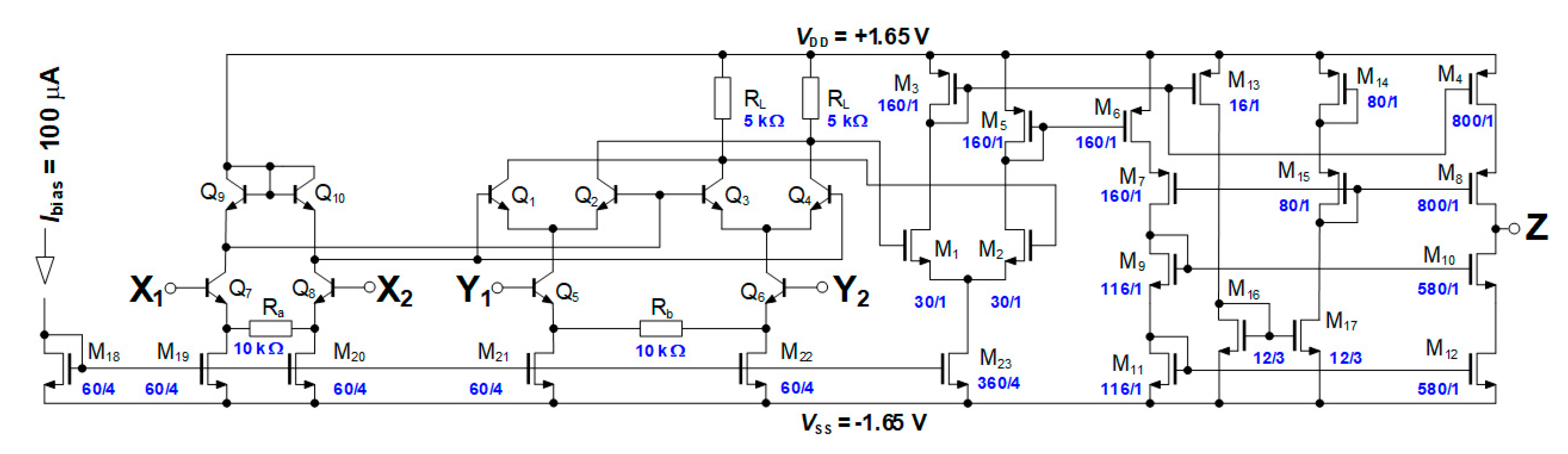
- A standard Gilbert core-based [49] BJT MLT was designed in order to obtain a more accurate device than the CMOS MLT (in general, the accuracy of the CMOS design is a problem). It has a larger transconductance constant and better symmetry of output swing currents than the CMOS MLT does. Moreover, our BJT MLT concept, compared to Reference [48], has a current output terminal instead of a voltage output terminal. Thanks to the presence of two multipliers (CMOS and BJT) in our IC package, an extension of the controllability of new advanced AEs is possible;
- (4)
- Compared to Reference [50], a modified CCCII cell topology with full mirroring of currents from differential stage (pair) to four output terminals is presented. The main innovation is in specific biasing current reference generation for output mirrors and driving the value of RX (which was not the intention of Reference [50]). In contrast to our solution, the concept in Reference [50] is not capable of providing a large dynamic range and output cascoding due to its bias sources (voltage drop in real MOS elements) when very low supply voltage used;
- (5)
- A current amplifier cell with a completely new topology, designed for low-power purposes, is presented. Good linearity in a dynamic range of ±200 µA, linear control of current gain, low input (around 1 Ω) and excellent output resistance, and low power consumption are the main advantages of the proposed concept.
1.2. Organization of the Paper
2. Related Solutions of Modular Concepts
- (a)
- (b)
- (c)
- (d)
- (e)
- (f)
- (a)
- Five various cells (independent active cells implementing four different types of operations) are available;
- (b)
- (c)
- Four independent electronically controllable parameters of three types (2 gm, RX, and B); and
- (d)
- Differential and summing voltage operations as well as multiplicative operations are available.
- (a)
- Continuous electronic control is not available (FPAAs are tunable digitally in discrete steps);
- (b)
- Not favorable frequency features (the expected speed of applications and operation of signal paths up to tens of kHz);
- (c)
- High power consumption (in hundreds of mW);
- (d)
- Not a fully analog solution (additional mixed-mode subsystems and control circuits, including a clock signal, are required in an IC), and therefore the overall complexity is much higher; and
- (e)
- A high cost of available development kits.
3. A Developed Integrated Device for the Modular Design of Active Elements
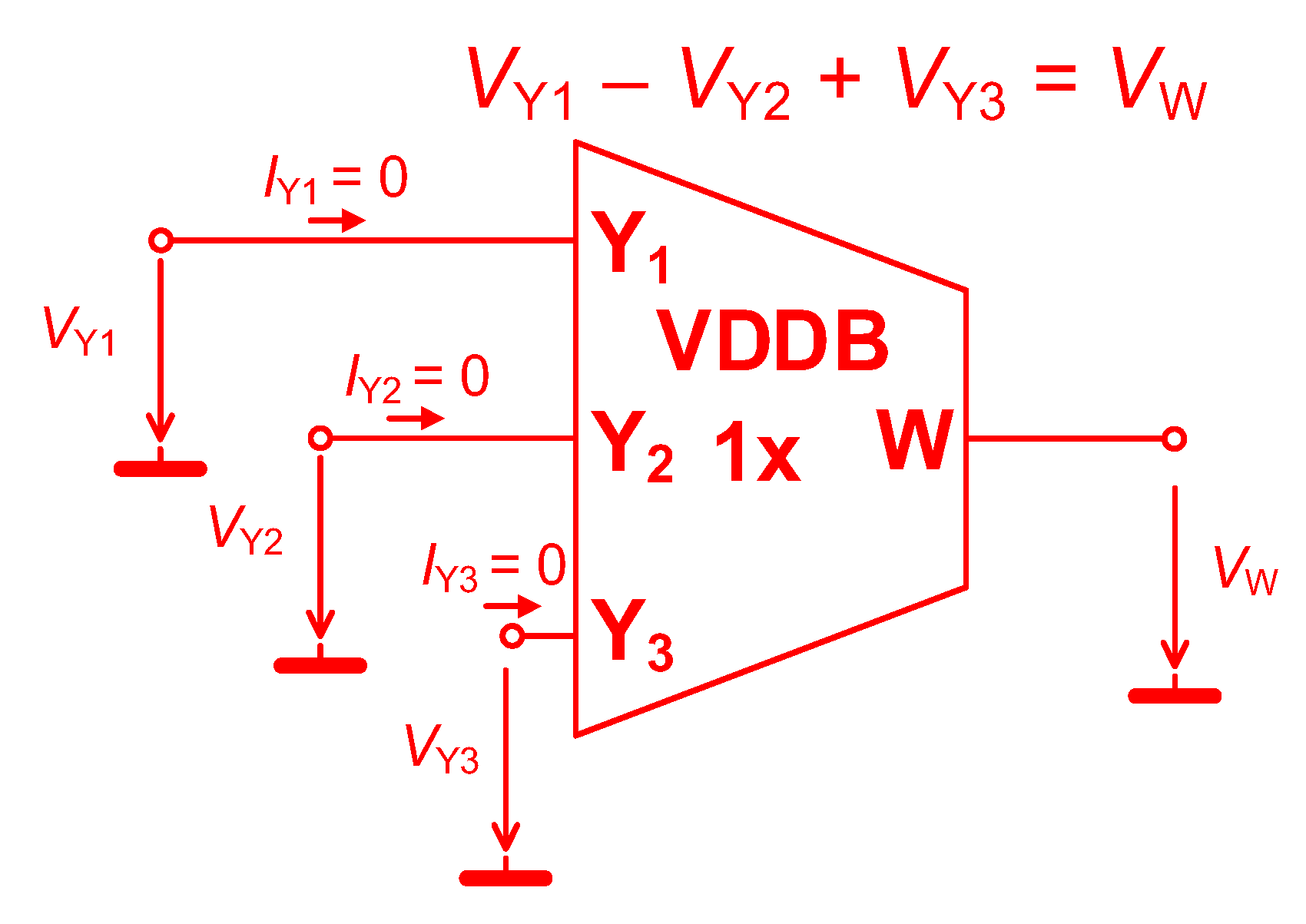
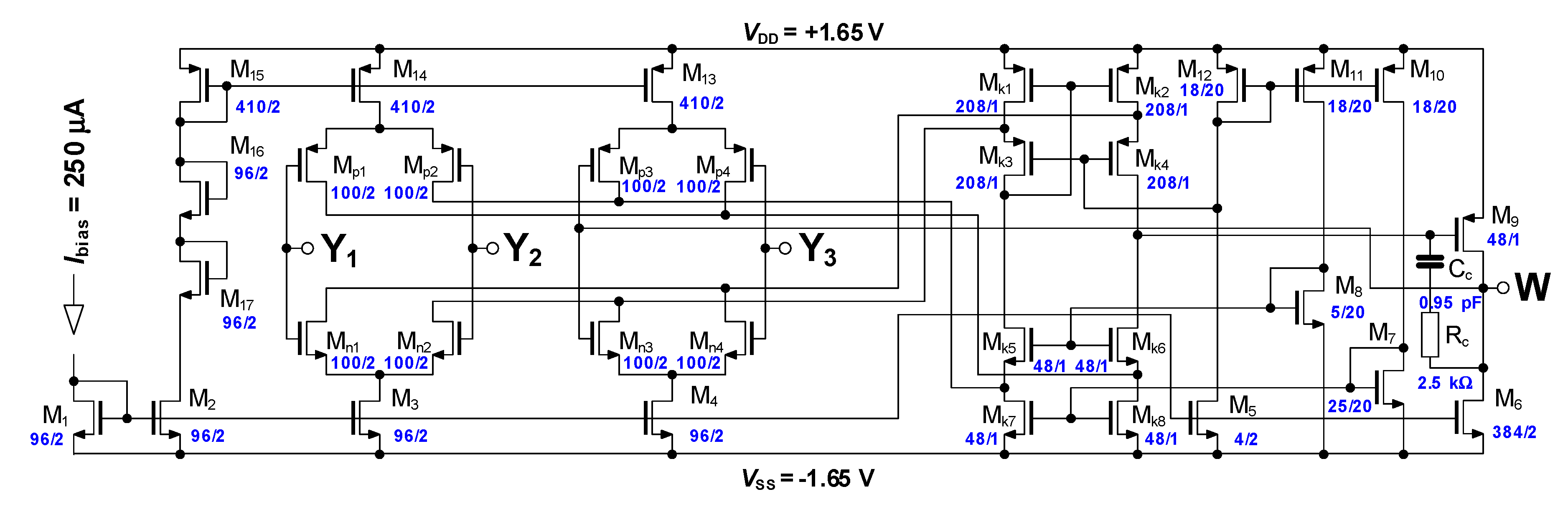
3.1. Voltage Differencing Differential Buffer (VDDB)
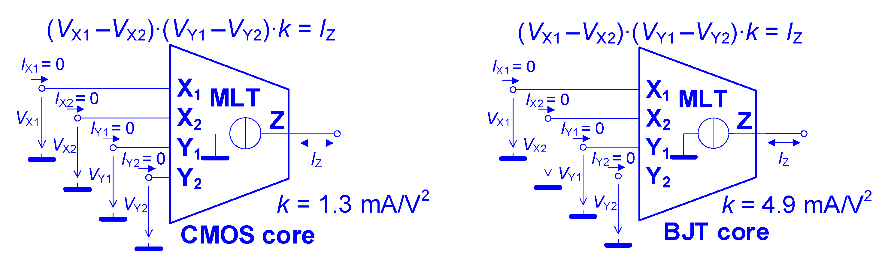
3.2. Voltage Multipliers with Current Output (CMOS MLT, BJT MLT)
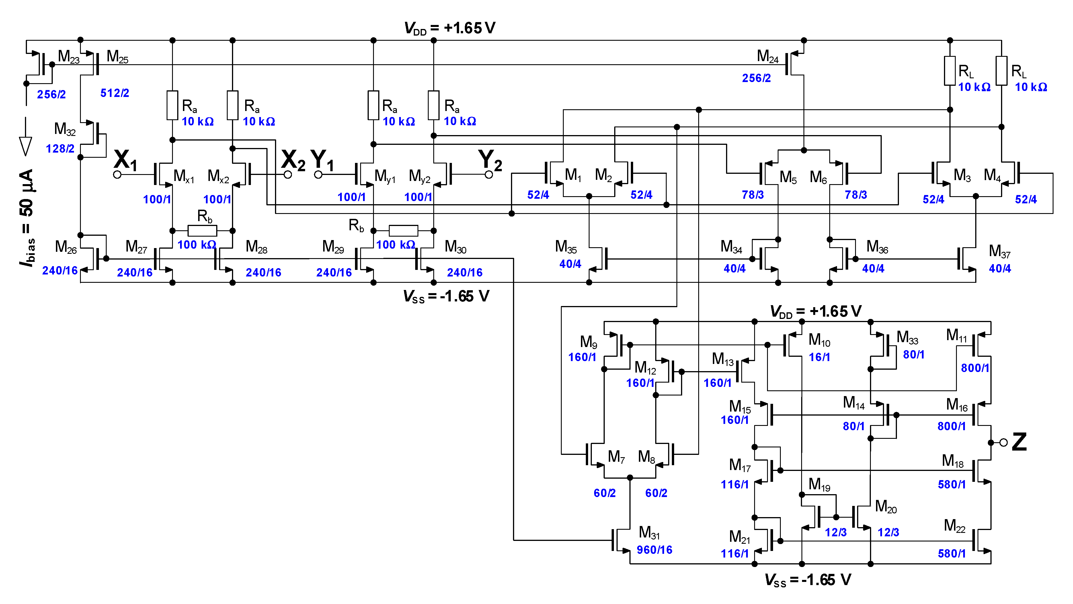
3.3. Current-Controlled Current Conveyor of the Second Generation (CCCII)
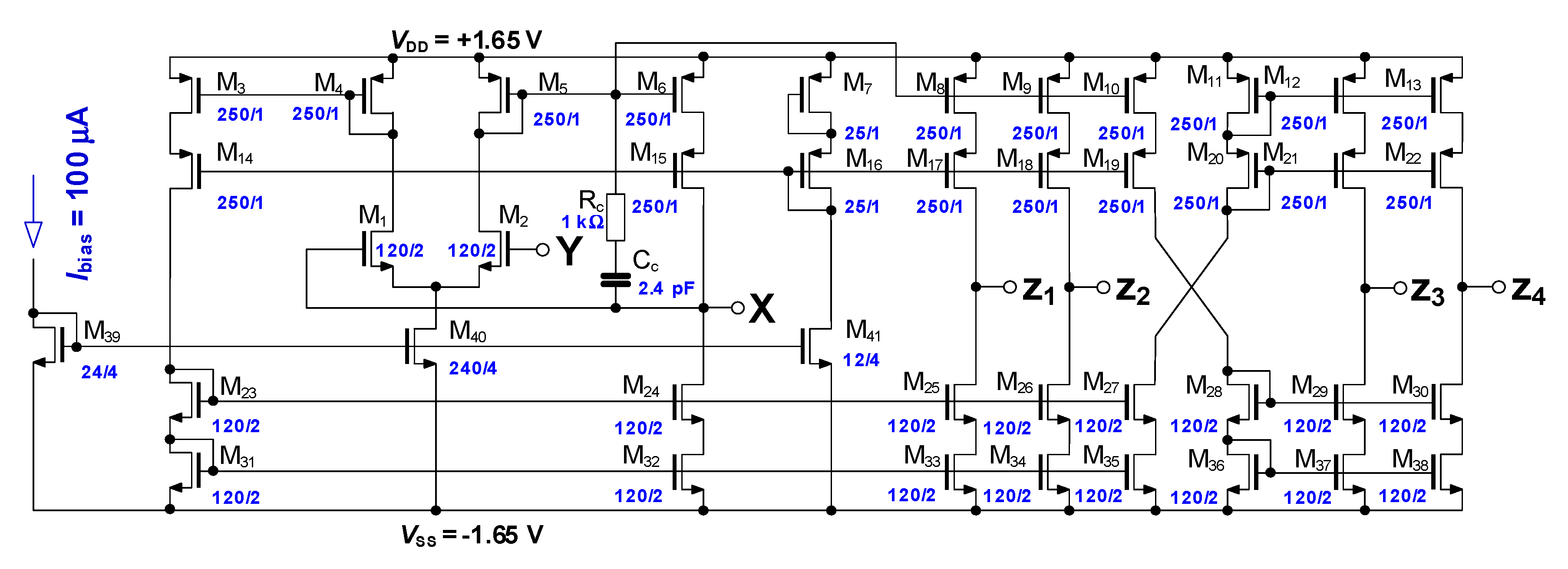
3.4. Current Amplifier with Controllable Current Gain (CA)
4. Experimentally Tested Features of the Proposed Cells
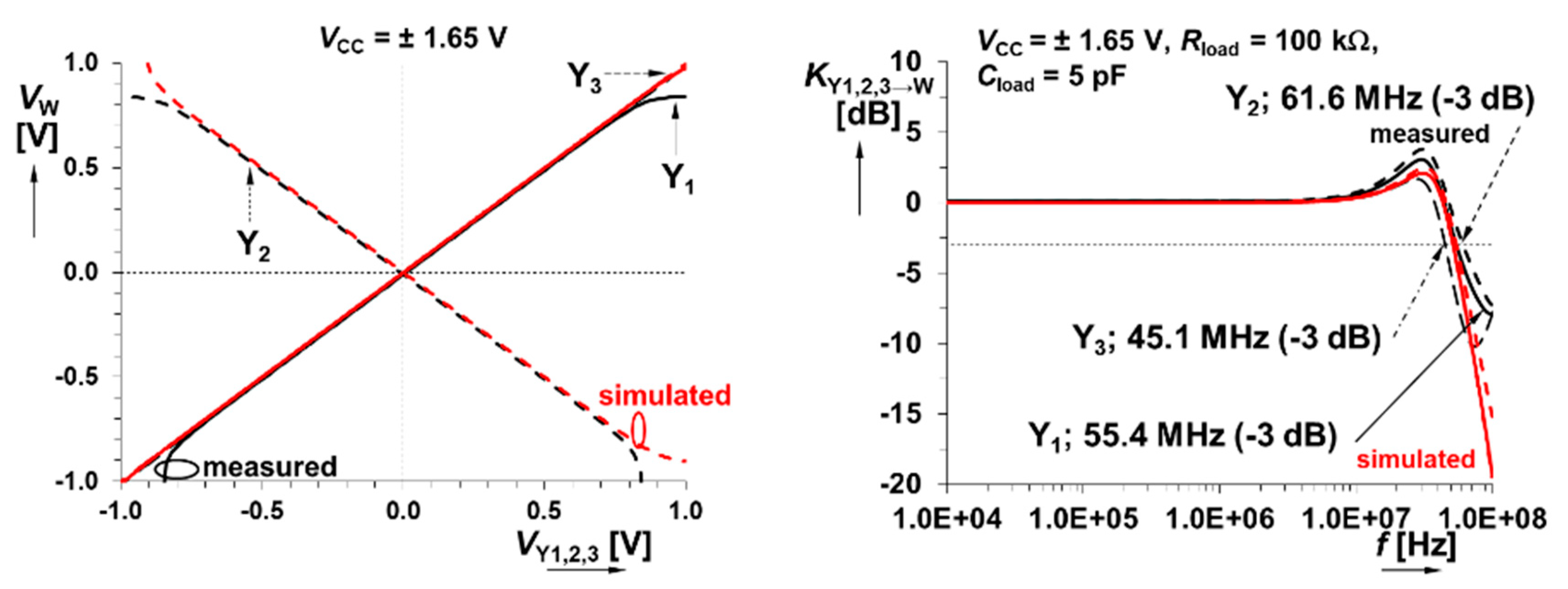
4.1. The VDDB
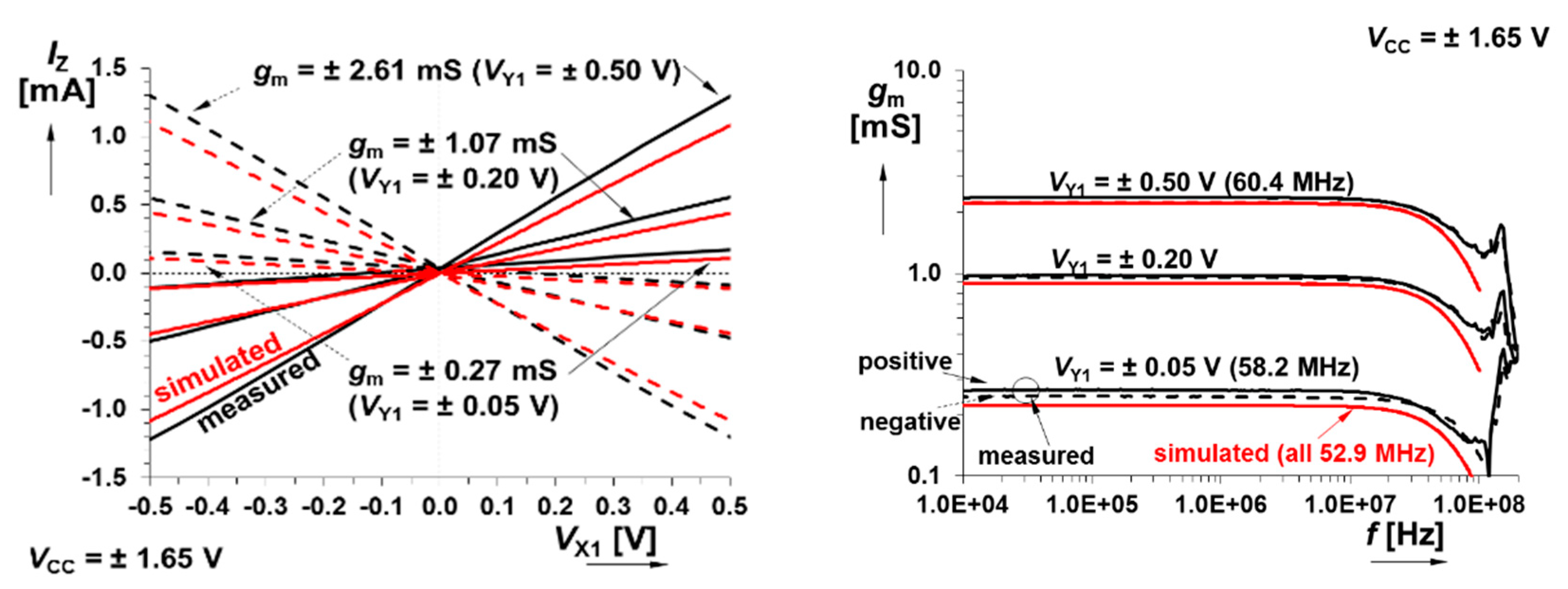
4.2. The CMOS MLT and BJT MLT
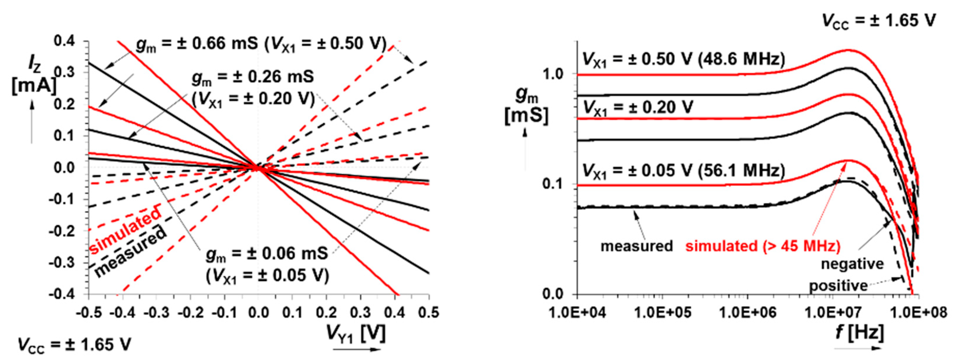
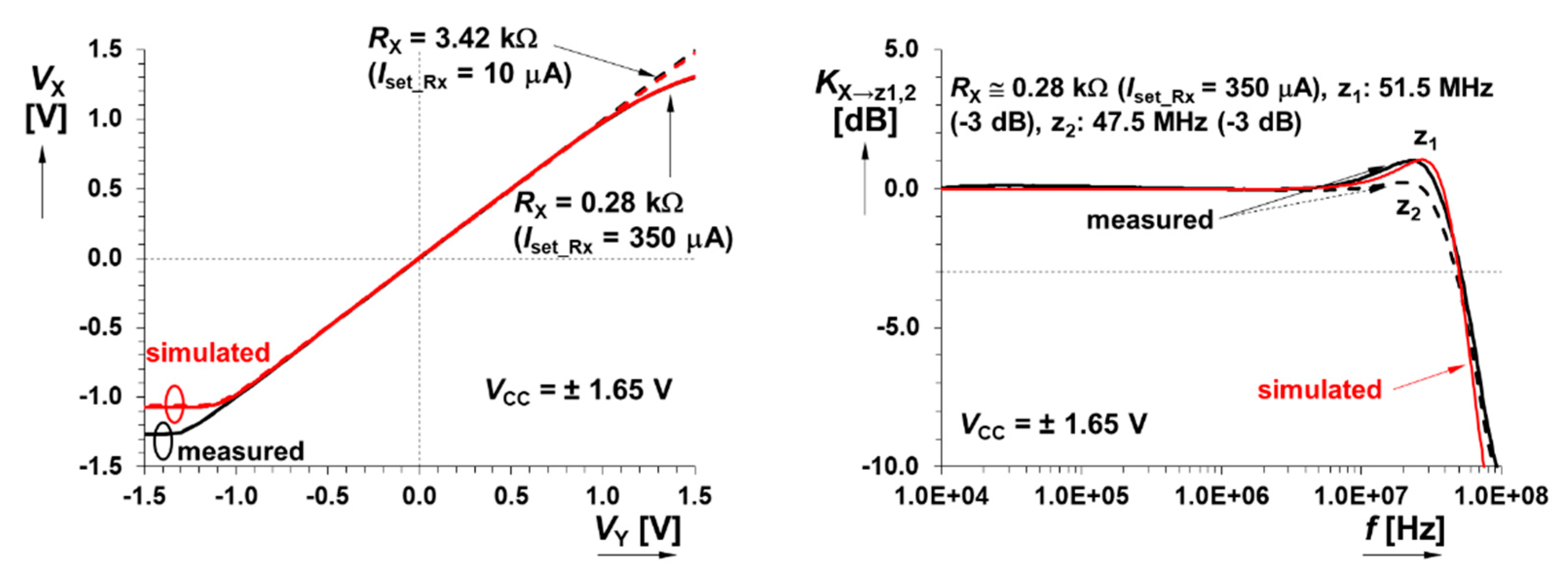
4.3. CCCII
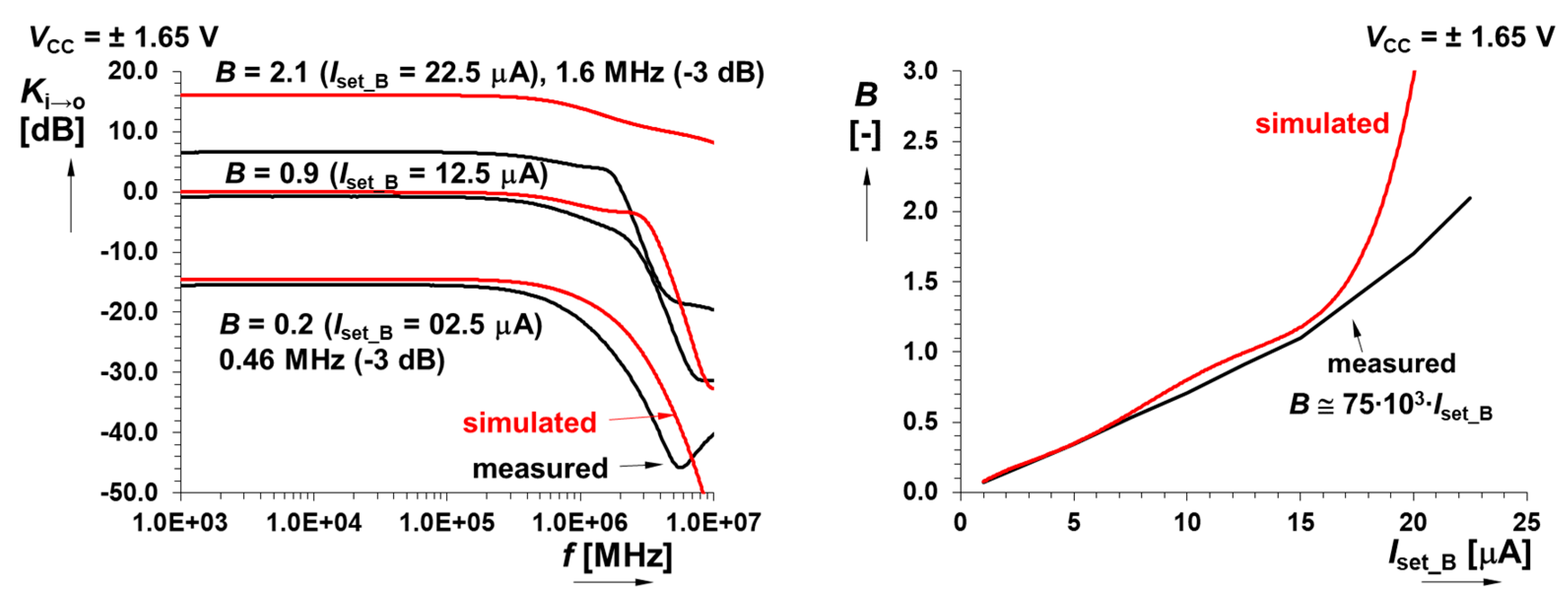
4.4. CA
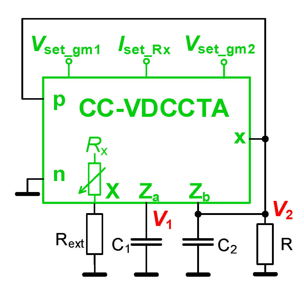
5. Example Interconnection of Internal Cells: A Novel Advanced Active Element
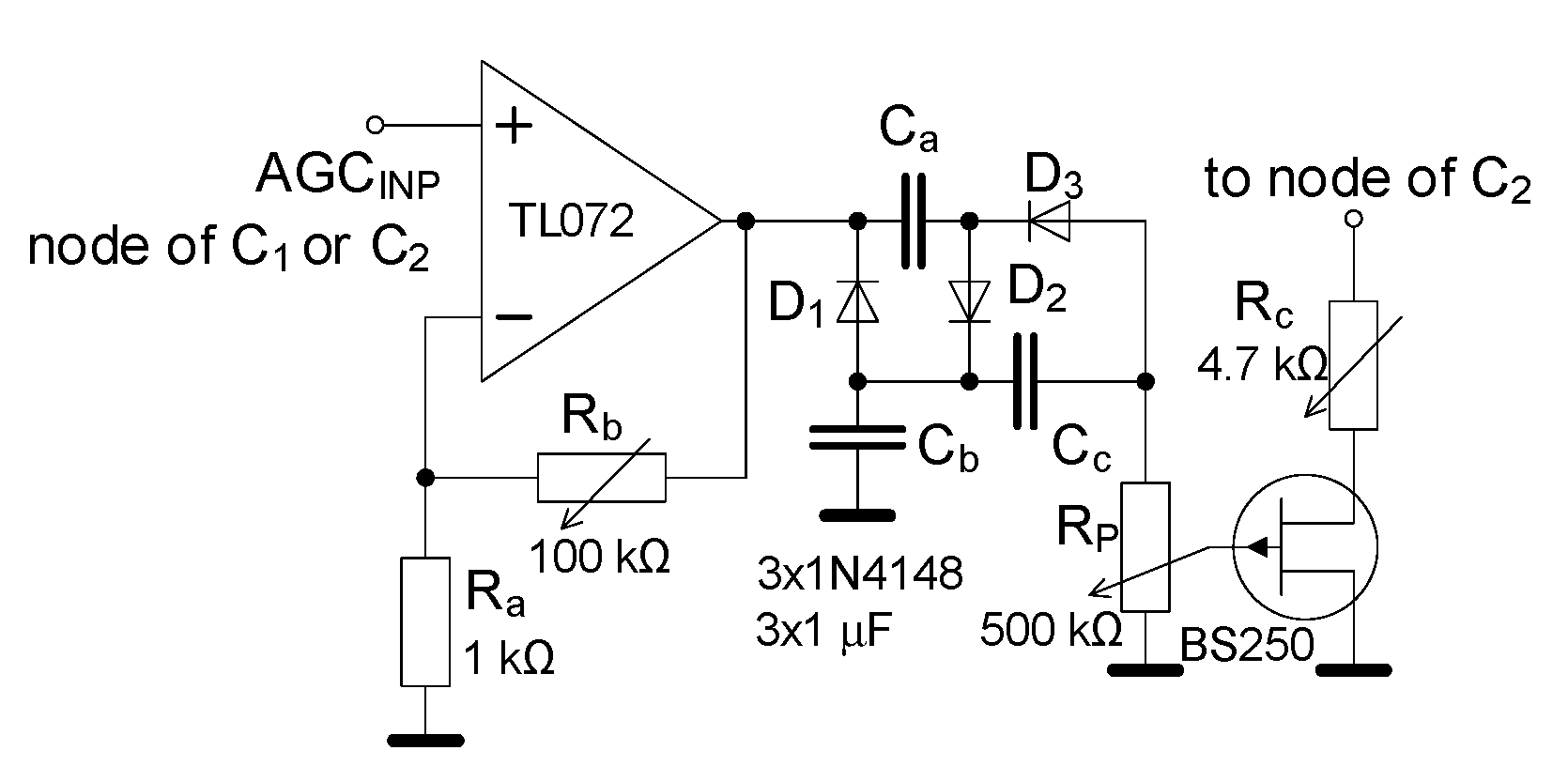
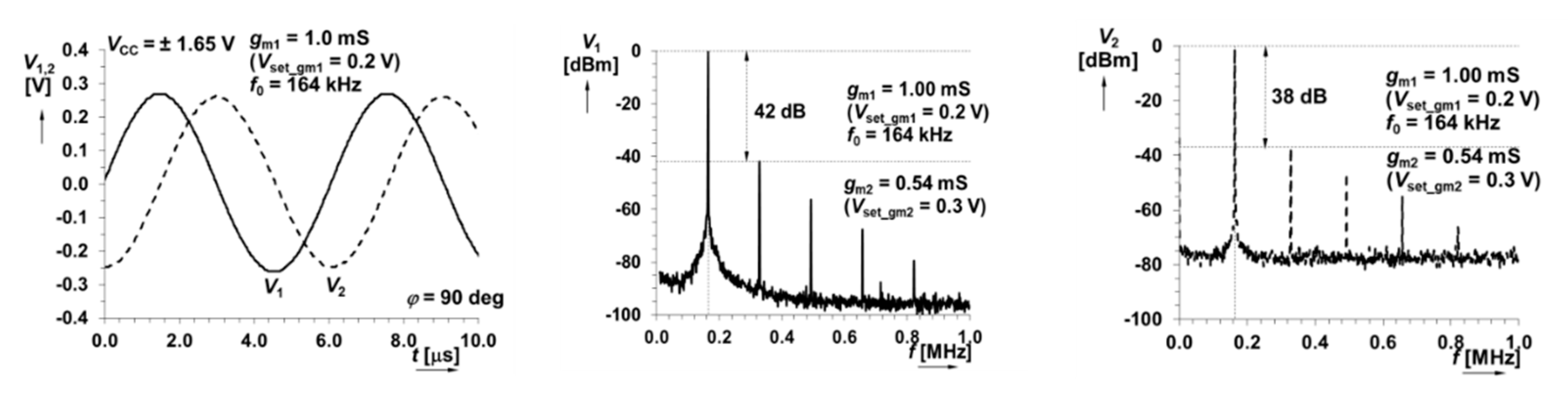
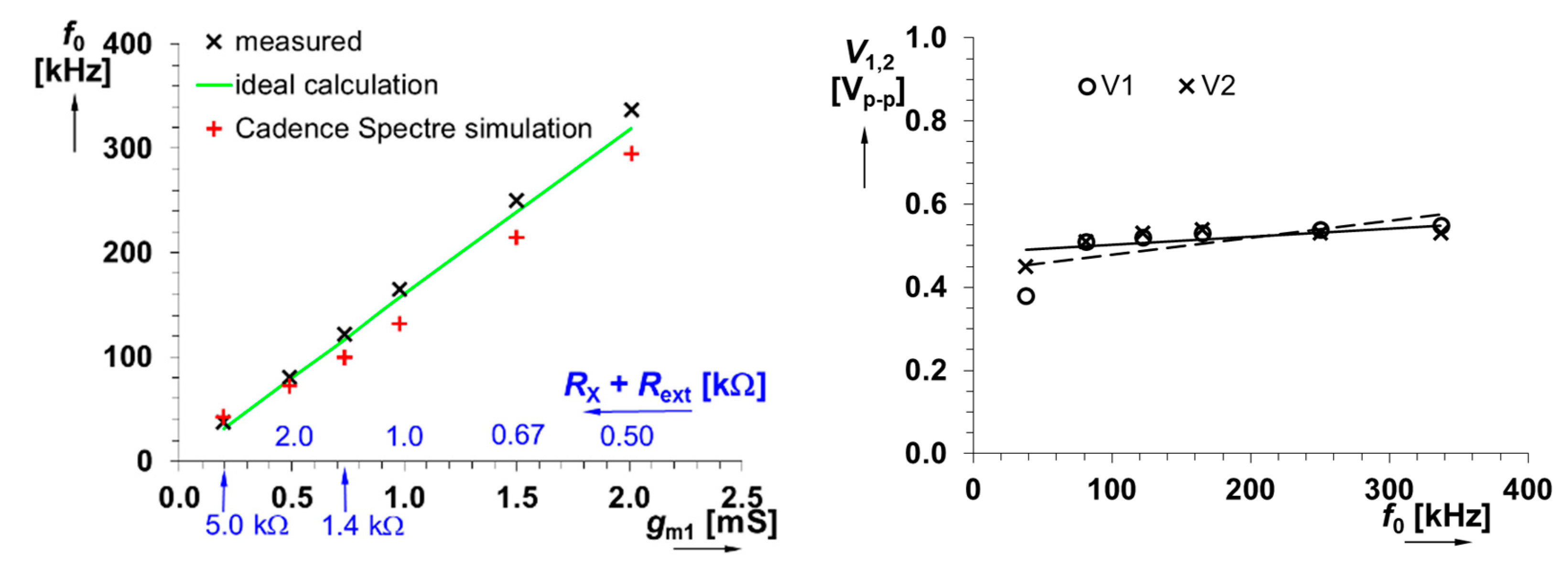
Application Example: CC-VDCCTA-Based Quadrature Oscillator
6. Conclusions
Author Contributions
Funding
Acknowledgments
Conflicts of Interest
Appendix A


| Parameters/Conditions | Simulation Results (Nominal Run) | Measured Results | Error (Measured vs Simulated) | Design Target |
|---|---|---|---|---|
| Small-signal AC transfer | ||||
| KY1 → W (−3 dB) | 1.00 [-] (51.6 MHz) | 1.02 [-] (55.4 MHz) | +2% (+7%) | 1 (≥30 MHz) |
| KY2 → W (−3 dB) | 1.00 [-] (54.3 MHz) | 1.02 [-] (61.6 MHz) | +2% (+13%) | 1 (≥30 MHz) |
| KY3 → W (−3 dB) | 1.00 [-] (51.3 MHz) | 1.01 [-] (45.1 MHz) | +1% (–12%) | 1 (≥30 MHz) |
| Input dynamic range | ||||
| Y1,2,3 → W | ≥ ±700 mV | ≥ ±700 mV | 0% | ≥±500 mV |
| Input DC offset (Monte Carlo) | ||||
| systematic + statistical (mismatch, 3 sigma; 99.7%) | real | |||
| Y1,3 → W | −0.57 ± 20.5 mV | |10| mV | expected statistical range | - |
| Y2 → W | −0.57 ± 20.5 mV | |10| mV | expected statistical range | - |
| Total harmonic distortion (for input voltage 500 mVpk-pk, 1 kHz) | ||||
| THD Y1,2,3→W | <0.10% | - | <1% | |
| Terminal impedances | ||||
| RY1,2,3, CY1,2,3 | ≥1 GΩ, 2.8 pF | 100 MΩ, 13 pF | - | >50 kΩ |
| RW, LW | 0.37 Ω, 4.3 µH | 0.54 Ω, 4.3 µH | - | <10 Ω |
| measured quiescent power consumption: 9.1 mW | ||||

| Parameters/Conditions | Simulation Results (Nominal Run) | Measured Results | Error (Measured vs Simulated) | Design Target |
|---|---|---|---|---|
| Small-signal AC transfer | ||||
| gm (X1 → Z) (−3 dB) for VY1 = ±0.05 → ±0.50 V | ±98 → ± 975 µS (≥53.0 MHz) | ±45 → ± 650 µS (≥30.0 MHz) | –54% → –33% (–43%) | ≥100 µS → ≥1000 µS (≥30 MHz) |
| gm (Y1 → Z) (−3 dB) for VX1 = ±0.05 → ±0.50 V | ±98 → ± 980 µS (≥44.0 MHz) | ±60 → ± 665 µS (≥44.0 MHz) | –39% → –32% (0%) | ≥100 µS → ≥1000 µS (≥30 MHz) |
| Input DC dynamic range | ||||
| X1 → Z for VY1 = ± 0.05 → ± 0.50 V | ≥±500 mV | ≥±500 mV | 0% | ≥±500 mV |
| Y1 → Z for VX1 = ± 0.05 → ± 0.50 V | ≥±600 mV | ≥±600 mV | 0% | ≥±500 mV |
| Input DC offset (Monte Carlo) | ||||
| systematic + statistical (mismatch, 3 sigma; 99.7%) | real maximum | |||
| X1 → Z for VY1 = ± 0.5 V | 3.3 ± 63 mV | |6| mV | expected statistical range | - |
| Y1 → Z for VX1 = ±0.5 V | 3.2 ± 66 mV | |18| mV | expected statistical range | - |
| Total harmonic distortion (for input voltage 500 mVpk-pk, 1 kHz) | ||||
| THD X1 → Z for VY1 = ± 0.1 V | ≤0.16% | - | <1% | |
| THD X1 → Z for VY1 = ± 0.5 V | ≤0.14% | - | <1% | |
| THD Y1 → Z for VX1 = ± 0.1 V | ≤1.45% | - | <1% | |
| THD Y1 → Zfor VX1 = ± 0.5 V | ≤0.45% | - | <1% | |
| Terminal impedances | ||||
| RX1, CX1 for all VY1 | ≥1 GΩ, 2.5 pF | 100 MΩ, 10–24 pF | - | >50 kΩ |
| RY1, CY1 for all VX1 | ≥1 GΩ, 2.5 pF | 100 MΩ, 14 pF | - | >50 kΩ |
| RZ, CZ for VX1 = ± 0.50 V | 1.55 MΩ, 5.3 pF | ≥100 kΩ, 16.2 pF | - | >50 kΩ |
| measured quiescent power consumption: 7.8 mW | ||||

| Parameters/Conditions | Simulation Results (Nominal Run) | Measured Results | Error (Measured vs Simulated) | Design Target |
|---|---|---|---|---|
| Small-signal AC transfer | ||||
| gm(X1 → Z) (-3 dB) for VY1 = ± 0.05 → ±0.50 V | ±222 → ±2220 µS (≥53.0 MHz) | ±250 → 2340 µS (≥52.0 MHz) | +13% → +5% (–2%) | ±200 → ± 2000 µS (≥30 MHz) |
| gm(Y1 → Z) (-3 dB) for VX1 = ±0.05 → ±0.50 V | ±222 → ±2210 µS (≥53.0 MHz) | ±250 → 2350 µS (≥39.0 MHz) | +13% → +6% (–26%) | ±200 → ± 2000 µS (≥30 MHz) |
| Input DC dynamic range | ||||
| X1 → Z for VY1 = ±0.05 → ±0.50 V | ≥±600 mV | ≥±700 mV | +17% | ≥±500 mV |
| Y1 → Z for VX1 = ±0.05 → ±0.50 V | ≥±600 mV | ≥±700 mV | +17% | ≥±500 mV |
| Input DC offset (Monte Carlo) | ||||
| systematic + statistical (mismatch, 3 sigma; 99.7%) | real maximum | |||
| X1 → Z for VY1 = ±0.5 V | −1.4 ± 29 mV | |14| mV | expected statistical range | - |
| Y1 → Z for VX1 = ±0.5 V | −1.3 ± 29 mV | |15| mV | expected statistical range | - |
| Total harmonic distortion (for input voltage 500 mVpk-pk, 1 kHz) | ||||
| THD X1 → Z for VY1 = ±0.1 V | ≤0.32% | - | <1% | |
| THD X1 → Z for VY1 = ±0.5 V | ≤0.47% | - | <1% | |
| THD Y1 → Z for VX1 = ±0.1 V | ≤0.17% | - | <1% | |
| THD Y1 → Zfor VX1 = ±0.5 V | ≤0.44% | - | <1% | |
| Terminal impedances | ||||
| RX1, CX1 for all VY1 | 129 kΩ, 2.8 pF | 176 kΩ, 18.3 pF | - | >50 kΩ |
| RY1, CY1 for all VX1 | 127 kΩ, 2.8 pF | 173 kΩ, 15.4 pF | - | >50 kΩ |
| RZ, CZ for VX1 = ±0.50 V | 803 kΩ, 3.9 pF | ≥100 kΩ, 16.1 pF | - | >50 kΩ |
| measured quiescent power consumption: 9.5 mW | ||||

| Parameters/Conditions | Simulation Results (Nominal Run with Input/Output Capacity 5 pF) | Measured Results | Error (Measured vs Simulated) | Design Target |
|---|---|---|---|---|
| Small-signal AC transfer | ||||
| KX → z1 (−3 dB) for Iset_Rx = 350 µA | 1.00 [-] (49.6 MHz) | 0.98 [-] (51.5 MHz) | –2% (+9%) | 1 (≥30 MHz) |
| KX → z2 (−3 dB) for Iset_Rx = 350 µA | 1.00 [-] (49.6 MHz) | 0.98 [-] (47.5 MHz) | –2% (–4%) | 1 (≥30 MHz) |
| KX → z3 (−3 dB) for Iset_Rx = 350 µA | 0.93 [-] (41.1 MHz) | 1.00 [-] (37.0 MHz) | +7% (–10%) | 1 (≥30 MHz) |
| KX → z4 (−3 dB) for Iset_Rx = 350 µA | 0.93 [-] (41.1 MHz) | 1.00 [-] (38.7 MHz) | +7% (–5%) | 1 (≥30 MHz) |
| KY → X (−3 dB) for Iset_Rx = 350 µA | 1.00 [-] (52.1 MHz) | 1.00 [-] (49.7 MHz) | 0% (–5%) | 1 (≥30 MHz) |
| GBWX → Z1 for Iset_Rx = 10→350 µA | 12.7 → 49.6 MHz | 11 → 51.5 MHz | –13% → +4% | - |
| GBWX → Z2 for Iset_Rx = 10→350 µA | 12.7 → 49.6 MHz | 9.8 → 47.5 MHz | –23% → –4% | - |
| GBWX → Z3 for Iset_Rx = 10→350 µA | 10.8 → 41.1 MHz | 7.8 → 37 MHz | –28% → –10% | - |
| GBWX → Z4 for Iset_Rx = 10→350 µA | 10.8 → 41.1 MHz | 8 → 38.7 MHz | –26% → –6% | - |
| GBWY → X for Iset_Rx = 10→350 µA | 11.9 → 52.1 MHz | 6.1 → 49.7 MHz | –49% → –5% | - |
| Input DC dynamic range | ||||
| X → Z1-4 for Iset_Rx = 10 → 350 µA | ±80 → ±1700 µA | ±99 → ±1700 µA | +24% → +0% | ±100 → ±1000 µA |
| Y → X for Iset_Rx = 10, 350 µA | ≥±500 mV | ≥±1000 mV | +100% | ≥±500 mV |
| Input DC offset (Monte Carlo) | ||||
| systematic + statistical (mismatch, 3 sigma; 99.7%) | real | |||
| X → Z1 for Iset_Rx = 100 µA | 0.047 ± 8.2 µA | −5.4 µA | expected stat. range | - |
| X → Z2 for Iset_Rx = 100 µA | 0.047 ± 8.2 µA | −0.05 µA | expected stat. range | - |
| X → Z3 for Iset_Rx = 100 µA | −0.043 ± 12.0 µA | 0.65 µA | expected stat. range | - |
| X → Z4 for Iset_Rx = 100 µA | −0.043 ± 12.0 µA | −0.64 µA | expected stat. range | - |
| Y → X for Iset_Rx = 100 µA | 0.336 ± 3.771 mV | 2.5 mV | expected stat. range | - |
| Total harmonic distortion | ||||
| THD X → z1,2 for Iset_Rx = 50, 350 µA (for input current 100 µApk-pk, 1 kHz) | 0.04, 0.07% | - | <1% | |
| THD X → z3,4 for Iset_Rx = 50, 350 µA (for input current 100 µApk-pk, 1 kHz) | 0.003, 0.11% | - | <1% | |
| THD Y → X for Iset_Rx = 50 and 200 µA (for input voltage 500 mVpk-pk, 1 kHz) | 0.08, 0.07% | - | <1% | |
| Terminal impedances | ||||
| RX, CX for Iset_Rx = 5 → 350 µA | 2320 → 240 Ω, 10 pF | 6670 → 280 Ω, 20 pF | +188% → +17% | 2500 → 250 Ω |
| RY, CY for all Iset_Rx | ≥1 GΩ, 2.7 pF | 100 MΩ,14.5 pF | - | >50 kΩ |
| Rz1,2, Cz1,2 for Iset_Rx = 5 µA | 52 MΩ, 4.8 pF | 100 MΩ, 15.9 pF | - | >50 kΩ |
| Rz1,2, Cz1,2 for Iset_Rx = 350 µA | 44 kΩ, 4.8 pF | 66 kΩ, 15.9 pF | - | >50 kΩ |
| Rz3,4, Cz3,4 for Iset_Rx = 5 µA | 106 MΩ, 2.5 pF | 100 MΩ, 15.9 pF | - | >50 kΩ |
| Rz3,4, Cz3,4 for Iset_Rx = 350 µA | 49 kΩ, 2.5 pF | 82 kΩ, 15.9 pF | - | >50 kΩ |
| measured quiescent power consumption: 16.8 mW | ||||

| Parameters/Conditions | Simulation Results (Nominal Run) | Measured Results | Error (Measured vs Simulated) | Design Target |
|---|---|---|---|---|
| Small-signal AC transfer | ||||
| K(i → o) [-] for Iset_B = 1→22.5 µA | 0.08 → 6.35 | 0.07 → 2.14 | –12% → –8% | 0.1 → 1.0 |
| K(i → o) [dB] (−3 dB) for Iset_B = 1 µA | –22.3 → 16 dB (0.69 → 2.89 MHz) | –23.4 → 6.6 dB (0.46 → 1.56 MHz) | –12% → –66% | |
| B [-] for Iset_B = 1 → 22.5 µA | 0.076 → 6.346 | 0.067 → 2.138 | +5% → –59% | |
| GBW i→o for Iset_B = 1 → 22.5 µA | 0.69 → 2.89 MHz | 0.46 → 1.56 MHz | –33% → –46% | ≥100 kHz |
| Input dynamic range | ||||
| I → o for Iset_B = 1 → 22.5 µA | ≥±200 µA | ≥±180 µA | –10% | ≥±150 µA |
| Input DC offset (systematic) | ||||
| I → o for Iset_B = 1 → 22.5 µA | 0.04 → 0.06 µA | 6 → −9 µA | expected stat. range | - |
| Total harmonic distortion (for input current 100 µA Apk-pk, 1 kHz) | ||||
| THD I → o for Iset_B = 12.5 µA | 0.14% | - | <1% | |
| Terminal (input/output) impedances | ||||
| Ri, Li for all Iset_B | 0.91 Ω, 31 µH | 1.4 Ω, 42 µH | - | <10 Ω |
| Ro, Co for Iset_B = 1 → 22.5 µA | 80 MΩ → 59 kΩ, 3.9 pF | 30 MΩ → 3 MΩ, 14.1 pF | - | >1 MΩ |
| measured quiescent power consumption: 1.7 mW | ||||
References
- Chen, W. The Circuits and Filters Handbook, 3rd ed.; CRC Press: Boca Raton, FL, USA, 2009; 3364p, ISBN 978-0849383410. [Google Scholar]
- Raut, R.; Swamy, M.N.S. Modern Analog Filter Analysis and Design: A practical approach, 1st ed.; Willey: Weinheim, Germany, 2010; 378p, ISBN 9783527407668. [Google Scholar]
- Senani, R.; Bhaskar, D.R.; Singh, A.K. Current Conveyors: Variants, Applications and Hardware Implementations, 1st ed.; Springer: Berlin, Germany, 2015; 560p, ISBN 978-3-319-08683-5. [Google Scholar]
- Senani, R.; Bhaskar, D.R.; Singh, A.K.; Sharma, R.K. Sinusoidal Oscillators and Waveform Generators using Modern Electronic Circuit Building Blocks, 1st ed.; Springer International Publishing: Cham, Switzerland, 2016; pp. 1–622. ISBN 978-3-319-23711-4. [Google Scholar]
- Xia, J.; Wang, Y.C.; Ma, F.C. Experimental demonstration of 1.5 GHz chaos generation using an improved Colpitts oscillator. Nonlinear Dyn. 2013, 72, 575–580. [Google Scholar] [CrossRef]
- Stork, M. Energy feedback used for oscillators control. Nonlinear Dyn. 2016, 85, 871–879. [Google Scholar] [CrossRef]
- Li, C.-H. RF Circuit Design; John Wiley and Sons, Inc.: Hoboken, NJ, USA, 2008; ISBN 9780470167588. [Google Scholar]
- Metin, B.; Arslan, E.; Herencsar, N.; Cicekoglu, O. Voltage-mode MOS-only all-pass filter. In Proceedings of the 2011 34th International Conference on Telecommunications and Signal Processing (TSP), Budapest, Hungary, 18–20 August 2011; pp. 317–318. [Google Scholar] [CrossRef]
- Metin, B.; Herencsar, N.; Cicekoglu, O. Low-Voltage Electronically Tunable MOSFET-C Voltage-Mode First-Order All-Pass Filter Design. Radioenginnering 2013, 22, 985–994. [Google Scholar]
- Ozenli, D.; Kuntman, H. MOS-only circuit design automation. In Proceedings of the 2016 IEEE 7th Latin American Symposium on Circuits & Systems (LASCAS), Florianopolis, Brazil, 28 February–2 March 2016; pp. 203–206. [Google Scholar] [CrossRef]
- Konal, M.; Kacar, F. MOS Only Grounded Active Inductor Circuits and Their Filter Applications. J. Circuits Syst. Comput. 2017, 26, 1750098. [Google Scholar] [CrossRef]
- Safari, L.; Yuce, E.; Minaei, S. A new low-power current-mode MOS only versatile precision rectifier. AEU Int. J. Electron. Commun. 2018, 83, 40–51. [Google Scholar] [CrossRef]
- Biolek, D.; Senani, R.; Biolkova, V.; Kolka, Z. Active elements for analog signal processing: Classification, Review and New Proposals. Radioengineering 2008, 17, 15–32. [Google Scholar]
- Kundert, K.; Chang, H.; Jefferies, D.; Lamant, G.; Malavasi, E.; Sending, F. Design of Mixed-Signal Systems-on-a-Chip. IEEE Trans. Comput. Aided Des. Integr. Circuits Syst. 2000, 19, 1561–1571. [Google Scholar] [CrossRef]
- Carter, B.; Brown, T.R. Handbook of Operational Amplifier Applications. Texas Instruments—Application Report 2016. pp. 1–94. Available online: http://www.ti.com/lit/an/sboa092b/sboa092b.pdf (accessed on 21 May 2019).
- Jerabek, J.; Sotner, R.; Vrba, K. Comparison of the SITO Current-Mode Universal Filters Using Multiple-Output Current Followers. In Proceedings of the 2012 35th International Conference on Telecommunications and Signal Processing (TSP), Prague, Czech Republic, 3–4 July 2012; pp. 406–410. [Google Scholar] [CrossRef]
- Sedra, A.; Smith, K.C. A second generation current conveyor and its applications. IEEE Trans. Circuit Theory 1970, 17, 132–134. [Google Scholar] [CrossRef]
- Svoboda, J.A.; McGory, L.; Webb, S. Applications of a commercially available current conveyor. Int. J. Electron. 2007, 70, 159–164. [Google Scholar] [CrossRef]
- Cajka, J.; Dostal, T.; Vrba, K. General view on current conveyors. Int. J. Circuit Theory Appl. 2004, 32, 133–138. [Google Scholar] [CrossRef]
- Biolek, D.; Biolkova, V. Implementation of active elements for analog signal processing by diamond transistors. In Proceedings of the International Conference on Electronic Devices and Systems (EDS’09 IMAPS CS), Brno, Czech Republic, 2 September 2009; pp. 304–309. [Google Scholar]
- Geiger, R.L.; Sanchez-Sinencio, E. Active filter design using operational transconductance amplifier: A tutorial. IEEE Circuits Devices Mag. 1985, 1, 20–32. [Google Scholar] [CrossRef]
- Sanchez-Sinencio, E.; Silva-Martinez, J. CMOS transconductance amplifiers, architectures and active filters: A tutorial. IEE Proc. Circuits Devices Syst. 2000, 147, 3–12. [Google Scholar] [CrossRef]
- Duong, Q.-H.; Le, Q.; Kim, C.-W.; Lee, S.-G. A 95-dB linear low-power variable gain amplifier. IEEE Trans. Circuits Syst. I Regul. Pap. 2006, 53, 1648–1657. [Google Scholar] [CrossRef]
- Hassan, T.M.; Mahmoud, S.A. New CMOS digitally controlled variable gain amplifier. In Proceedings of the 2008 International Conference on Microelectronics, Sharjah, UAE, 14–17 December 2008; pp. 23–28. [Google Scholar] [CrossRef]
- Texas Instruments. VCA810 High Gain Adjust Range, Wideband and Variable Gain Amplifier. Datasheet. 2015. Available online: http://www.ti.com/lit/ds/symlink/vca810.pdf (accessed on 21 May 2019).
- Fabre, A.; Saaid, O.; Wiest, F.; Boucheron, C. High frequency applications based on a new current controlled conveyor. IEEE Trans. Circuits Syst. I Regul. Pap. 1996, 43, 82–91. [Google Scholar] [CrossRef]
- Surakampontorn, W.; Thitimajshima, W. Integrable electronically tunable current conveyors. IEEE Proc. G Electron. Circuits Syst. 1988, 135, 71–77. [Google Scholar] [CrossRef]
- Fabre, A.; Mimeche, N. Class A/AB second-generation current conveyor with controlled current gain. Electron. Lett. 1994, 30, 1267–1269. [Google Scholar] [CrossRef]
- Minaei, S.; Sayin, O.K.; Kuntman, H. A new CMOS electronically tunable current conveyor and its application to current-mode filters. IEEE Trans. Circuits Syst. I Regul. Pap. 2006, 53, 1448–1457. [Google Scholar] [CrossRef]
- De Marcellis, A.; Ferri, G.; Guerrini, N.C.; Scotti, G.; Stornelli, V.; Trifiletti, A. The VGC-CCII: A novel building block and its application to capacitance multiplication. Analog Integr. Circuits Signal Process. 2009, 58, 55–59. [Google Scholar] [CrossRef]
- Kumngern, M.; Junnapiya, S. A sinusoidal oscillator using translinear current conveyors. In Proceedings of the 2010 IEEE Asia Pacific Conference on Circuits and Systems (APPCAS), Kuala Lumpur, Malaysia, 6–9 December 2010; pp. 740–743. [Google Scholar] [CrossRef]
- Sotner, R.; Kartci, A.; Jerabek, J.; Herencsar, N.; Dostal, T.; Vrba, K. An Additional Approach to Model Current Followers and Amplifiers with Electronically Controllable Parameters from Commercially Available ICs. Meas. Sci. Rev. 2012, 12, 255–265. [Google Scholar] [CrossRef]
- Jerabek, J.; Sotner, R.; Kartci, A.; Herencsar, N.; Dostal, T.; Vrba, K. Two Behavioral Models of the Electronically Controlled Generalized Current Conveyor of the Second Generation. In Proceedings of the 2015 38th International Conference on Telecommunications and Signal Processing (TSP), Prague, Czech Republic, 9–11 July 2015; pp. 349–353. [Google Scholar] [CrossRef]
- Sotner, R.; Herencsar, N.; Jerabek, J.; Langhammer, L.; Polak, J. On practical construction of electronically controllable compact current amplifier based on commercially available elements and its application. AEU Int. J. Electron. Commun. 2017, 81, 56–66. [Google Scholar] [CrossRef]
- Sotner, R.; Petrzela, J.; Domansky, O.; Langhammer, L.; Dostal, T. Single Active Parameter Tunable Simple Band-Pass Filter: Methods for Tunability Range Extension. In Proceedings of the 2017 24th International Conference Mixed Design of Integrated Circuits and Systems (MIXDES), Bydgoszcz, Poland, 22–24 June 2017; pp. 318–323. [Google Scholar] [CrossRef]
- Sotner, R.; Jerabek, J.; Prokop, R.; Kledrowetz, V. Simple CMOS voltage differencing current conveyor- based electronically tunable quadrature oscillator. Electron. Lett. 2016, 52, 1016–1018. [Google Scholar] [CrossRef]
- Sotner, R.; Jerabek, J.; Prokop, R.; Kledrowetz, V.; Polak, J.; Fujcik, L.; Dostal, T. Practically Implemented Electronically Controlled CMOS Voltage Differencing Current Conveyor. In Proceedings of the 2016 IEEE 59th International Midwest Symposium on Circuits and Systems (MWSCAS), Abu Dhabi, UAE, 16–19 October 2016; pp. 667–670. [Google Scholar] [CrossRef]
- Analog Devices. AD844 60 MHz, 2000 V/us Monolithic Op Amp with Quad Low Noise. Datasheet. 2017. Available online: http://www.analog.com/media/en/technical-documentation/data-sheets/AD844.pdf (accessed on 21 May 2019).
- Sponar, R.; Vrba, K. Measurements and Behavioral Modelling of Modern Conveyors. Int. J. Comput. Sci. Netw. Secur. 2006, 3, 57–63. [Google Scholar]
- Sponar, R.; Vrba, K.; Kubanek, D. Universal Current Conveyor and Universal Voltage Conveyor Measurement and Modeling. In Proceedings of the International Conference on Networking, International Conference on Systems and International Conference on Mobile Communications and Learning Technologies (ICNICONSMCL’06), Morne, Mauritius, 23–29 April 2006; pp. 1–4. [Google Scholar] [CrossRef]
- Prokop, R.; Musil, V. Modular approach to design of modern circuit blocks for current signal processing and new device CCTA. In Proceedings of the 7th International Conference on Signal and Image Processing, Honolulu, HI, USA, 15–17 August 2005; pp. 494–499. [Google Scholar]
- Prokop, R.; Musil, V. New modular current devices for true current mode signal processing. Electronics 2007, 16, 36–42. [Google Scholar]
- Sotner, R.; Herencsar, N.; Jerabek, J.; Prokop, R.; Kartci, A.; Dostal, T.; Vrba, K. Z-Copy Controlled-Gain Voltage Differencing Current Conveyor: Advanced Possibilities in Direct Electronic Control of First- Order Filter. Elektronika Ir Elektrotechnika 2014, 20, 77–83. [Google Scholar] [CrossRef]
- ON Semiconductor. I3T Process Technology. Available online: http://www.europractice-ic.com/technologies_AMIS_tech.php (accessed on 21 May 2019).
- Razavi, B. Design of Analog CMOS Integrated Circuits, 2nd ed.; McGraw-Hill: New York, NY, USA, 2016; 800p, ISBN 978-0072380323. [Google Scholar]
- Gray, P.R.; Hurst, P.J.; Lewis, S.H.; Meyer, R.G. Analysis and Design of Analog Integrated Circuits, 5th ed.; John Wiley and Sons, Inc.: Hoboken, NJ, USA, 2009; p. 896. ISBN 978-0470245996. [Google Scholar]
- Herencsar, N.; Sotner, R.; Metin, B.; Koton, J.; Vrba, K. VDDDA-New ‘Voltage Differencing’ Device for Analog Signal Processing. In Proceedings of the 2013 8th International Conference on Electrical and Electronics Engineering (ELECO), Bursa, Turkey, 28–30 November 2013; pp. 17–20. [Google Scholar] [CrossRef]
- Jasielsky, J.; Kuta, S.; Machowski, W.; Kolodziejski, W. Four-quadrant CMOS transconductance multiplier operating at low voltage and high-speed. In Proceedings of the 17th International Conference Mixed Design of Integrated Circuits and Systems (MIXDES), Warsaw, Poland, 24–26 June 2010; pp. 265–268. [Google Scholar]
- Gilbert, B. A high-performance monolithic multiplier using active feedback. IEEE J. Solid-State Circuits 1974, 9, 364–373. [Google Scholar] [CrossRef]
- Ferri, G.; Guerrini, N.C. Low-Voltage Low-Power CMOS Current Conveyors, 1st ed.; Kluwer Academic Publishers: London, UK, 2003; 220p, ISBN 978-1-4020-7486-8. [Google Scholar]
- Duarte-Villasenor, M.A.; Tlelo-Cuautle, E.; de la Fraga, L.G. Binar Genetic Encoding for Synthesis of Mixed-Mode Circuit Topologies. Circuits Syst. Signal Process. 2012, 31, 849–863. [Google Scholar] [CrossRef]
- Fakhfakh, M.; Pierzchala, M. Pathological Elements in Analog Circuit Design, 1st ed.; Lecture Notes in Electrical Engineering; Springer: Cham, Switzerland, 2018; 360p, ISBN 978-3-319-75156-6. [Google Scholar]
- Malcher, A.; Falkowski, P. Analog Reconfigurable Circuits. Int. J. Electron. Telecommun. 2014, 60, 8–19. [Google Scholar] [CrossRef][Green Version]
- TleTlelo-Cuautle, E.; de la Fraga, L.G.; Phanrattanachai, K.; Pitaksuttayaprot, K. CDCTA and OTA Realization of a Multi-phase Sinusoidal Oscillator. IETE Tech. Rev. 2015, 32, 497–504. [Google Scholar] [CrossRef]
- Sotner, R.; Jerabek, J.; Petrzela, J.; Herencsar, N.; Prokop, R.; Vrba, K. Second-order Simple Multiphase Oscillator Using Z-Copy Controlled-Gain Voltage Differencing Current Conveyor. Elektronika Ir Elektrotechnika 2014, 20, 13–18. [Google Scholar] [CrossRef]
- Pourak, T.; Suwanjan, P.; Jaikla, W.; Maneewan, S. Simple quadrature sinusoidal oscillator with orthogonal control using sigle active element. In Proceedings of the 2012 IEEE International Conference on Electron Devices and Solid State Circuit (EDSSC), Bangkok, Thailand, 3–5 December 2012; pp. 1–4. [Google Scholar] [CrossRef]
- Uttaphut, P. New Current-mode Quadrature Sinusoidal Oscillator Using Single DVCCTA as Active Element. Przeglad Eletrotechniczny 2016, 92, 229–232. [Google Scholar] [CrossRef][Green Version]
- Yesil, A.; Konal, M.; Kacar, F. Electronically Tunable Quadrature Oscillator Employing Single Differential Difference Transconductance Amplifier. Acta Phys. Pol. A 2017, 132, 843–845. [Google Scholar] [CrossRef]
- Linares-Barranco, B.; Rodriguez-Vazquez, A.; Sanchez-Sinencio, E.; Huertas, J.L. CMOS OTA-C high-frequency sinusoidal oscillators. IEEE J. Solid-State Circuits 1991, 26, 160–165. [Google Scholar] [CrossRef]
- Senani, R.; Bhaskar, D.R.; Gupta, M.; Singh, A.K. Canonic OTA-C Sinusoidal Oscillators: Generation of New Grounded-Capacitor Versions. Am. J. Electr. Electron. Eng. 2015, 3, 137–146. [Google Scholar] [CrossRef]


| References | Number of Cells (Internal Subparts) | Types of Cells (Number and Purpose of Terminals) | Independent Cells (No Internal Interconnection) | Variability in Interconnection | Electronically Controllable Parameters | Number of Electronically Controllable Parameters | Types of Electronically Controllable Parameters | Differential/Summing Voltage Operations Available | Multiplicative Operations | Technology (Fabrication Process) |
|---|---|---|---|---|---|---|---|---|---|---|
| [20] | 2 | 1 current conveyor (1 voltage input, 1 current input, 1 current output); | Yes | Yes | No | 0 | - | No | No | BJT commercial |
| 1 voltage buffer (1 input, 1 output) | ||||||||||
| [36,37] | 2 | 1 current-controlled current conveyor (1 voltage input, 1 current input, 2 current outputs); | Yes | Yes | Yes | 2 | 1 gm, 1 RX | No | Yes | CMOS 0.7-µm |
| 1 CMOS multiplier (4 voltage inputs, 1 current output) | ||||||||||
| [38] | 2 | 1 current conveyor (1 voltage input, 1 current input, 1 current output); | No | No | No | 0 | - | No | No | BJT commercial |
| 1 voltage buffer (1 input, 1 output) | ||||||||||
| [39,40] | 2 | 1 universal multiterminal current conveyor (3 voltage inputs, 1 current input, 4 current outputs); | Yes | Yes | No | 0 | - | Yes | No | CMOS 0.35-µm |
| 1 current conveyor (1 voltage input, 1 current input, 1 current output) | ||||||||||
| [41] | 2 | 1 current conveyor (1 voltage input, 1 current input, 1 current output); | Yes | Yes | Yes | 1 | gm | No | No | CMOS 0.7-µm |
| 1 OTA stage (2 voltage inputs, 1 current output) | ||||||||||
| [42] | 5 | 2 current differentiators (2 current inputs, 1 current output); 2 current conveyors (1 voltage input, 1 current input, 1 current output); | Yes | Yes | Yes | 4 | gm | No | No | CMOS 0.7-µm |
| 1 OTA stage (2 voltage inputs, 1 current output) | ||||||||||
| This work | 5 | 1 VDDB (3 voltage inputs, 1 voltage output); | Yes | Yes | Yes | 4 | 2 gm, 1 RX, 1 B | Yes | Yes | CMOS/BJT 0.35-µm |
| 1 current-controlled current conveyor (1 voltage input, 1 current input, 4 current outputs); | ||||||||||
| 1 CMOS multiplier (4 voltage inputs, 1 current output); | ||||||||||
| 1 BJT multiplier (4 voltage inputs, 1 current output); 1 current amplifier (1 current input, 1 current output) |
| References | Active Elements | No. of Auxiliary High Impedance Terminals Z | No. of Controllable Parameters of Device | No. of Passive Elements | Parameters for f0 Control | Trend of Electronic Tunability | Fulfillment of CO Given by Parameter | No. of Parameters Suitable for CO Control | FO and CO Fully Uncoupled | Constant Output Amplitude While f0 Is Tuned | Chip Area/Cell Area (mm2) | Power Consumption (Full IC/ Cells) (mW) |
|---|---|---|---|---|---|---|---|---|---|---|---|---|
| [36] | VDCC | 1 | 2 | 4 | gm | nonlinear | R valuea | 1 | Yes | No | 4/0.79 | -/45 |
| [55] | ZC-CG-VDCC | 1 | 3 | 4 | gm, RX | linear | B | 1 | Yes | Nob | N/A | -/7 |
| [56] | VDTA | 1 | 2 | 3 | gm | nonlinear | R valuea | 1 | Yes | No | N/A | N/A |
| [57] | DVCCTA | 1 | 1c | 5 | gm, RX | N/A | R valuea | 2 | Yes | N/A | N/A | N/A |
| [58] | DDTA | 1 | 1 | 3 | gm | nonlinear | C value | 0 | No | N/A | N/A | N/A |
| Figure 11 | CC-VDCCTA | 2 | 3 | 4 | gm1, RX | linear | gm2, R valuea | 2 | Yes | Yes | 2.34/0.35 | 45/34 |
| Cell | Frequency Features (Bandwidth) a | DC Features and Linearity (Dynamics) | Input Impedance | Output Impedance | Quiescent Power Consumption a | Accuracy of Simulation Results with Results of Experiments (Design Stage) |
|---|---|---|---|---|---|---|
| VDDB | Good (>45 MHz) | Good (±700 mV) | High (100 MΩ) | Low (good) (0.5 Ω) | Average (9.1 mW) | High |
| CMOS MLT | Average (>30 MHz) | Good (±500 mV) | High (100 MΩ) | Average (>100 kΩ) | Average (7.8 mW) | Within expected range (process variation) |
| BJT MLT | Good (>40 MHz) | Good (±700 mV) | Average (170 kΩ) | Average (>100 kΩ) | Average (9.5 mW) | Good |
| CCCII | Good (>37 MHz) | Good (±500 mV, Y) (to ±1700 µA, X) | High (100 MΩ, Y) Average (0.28 → 3.4 kΩ, X) | Average (>60 kΩ) | High (16.8 mW) | Good |
| CA | Low (<1.6 MHz) | Average (but excellent linearity) (±180 µA) | Low b (1.4 Ω) | High (good) (>3 MΩ) | Low (1.7 mW) | Average |
© 2019 by the authors. Licensee MDPI, Basel, Switzerland. This article is an open access article distributed under the terms and conditions of the Creative Commons Attribution (CC BY) license (http://creativecommons.org/licenses/by/4.0/).
Share and Cite
Sotner, R.; Jerabek, J.; Polak, L.; Prokop, R.; Kledrowetz, V. Integrated Building Cells for a Simple Modular Design of Electronic Circuits with Reduced External Complexity: Performance, Active Element Assembly, and an Application Example. Electronics 2019, 8, 568. https://doi.org/10.3390/electronics8050568
Sotner R, Jerabek J, Polak L, Prokop R, Kledrowetz V. Integrated Building Cells for a Simple Modular Design of Electronic Circuits with Reduced External Complexity: Performance, Active Element Assembly, and an Application Example. Electronics. 2019; 8(5):568. https://doi.org/10.3390/electronics8050568
Chicago/Turabian StyleSotner, Roman, Jan Jerabek, Ladislav Polak, Roman Prokop, and Vilem Kledrowetz. 2019. "Integrated Building Cells for a Simple Modular Design of Electronic Circuits with Reduced External Complexity: Performance, Active Element Assembly, and an Application Example" Electronics 8, no. 5: 568. https://doi.org/10.3390/electronics8050568
APA StyleSotner, R., Jerabek, J., Polak, L., Prokop, R., & Kledrowetz, V. (2019). Integrated Building Cells for a Simple Modular Design of Electronic Circuits with Reduced External Complexity: Performance, Active Element Assembly, and an Application Example. Electronics, 8(5), 568. https://doi.org/10.3390/electronics8050568